manuals.online logo
Brands
  1. Home
  2. •
  3. Brands
  4. •
  5. Sony
  6. •
  7. CD Player
  8. •
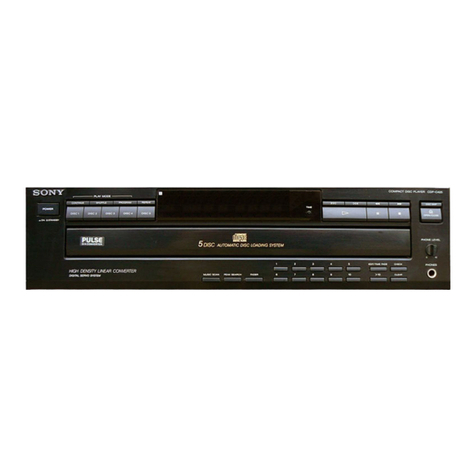
  9. Sony CDP-C320M User manual

Sony CDP-C320M User manual

This manual suits for next models

1

Other Sony CD Player manuals

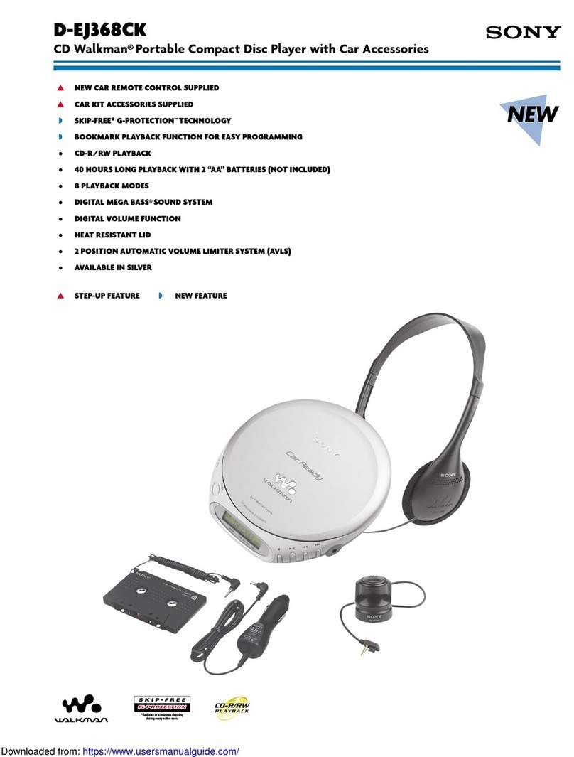
Sony CFD-565 User manual

Sony

Sony CFD-565 User manual

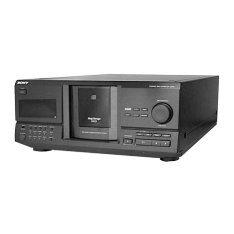
Sony CDP-CX350 - 300 Disc Cd Changer User manual

Sony

Sony CDP-CX350 - 300 Disc Cd Changer User manual

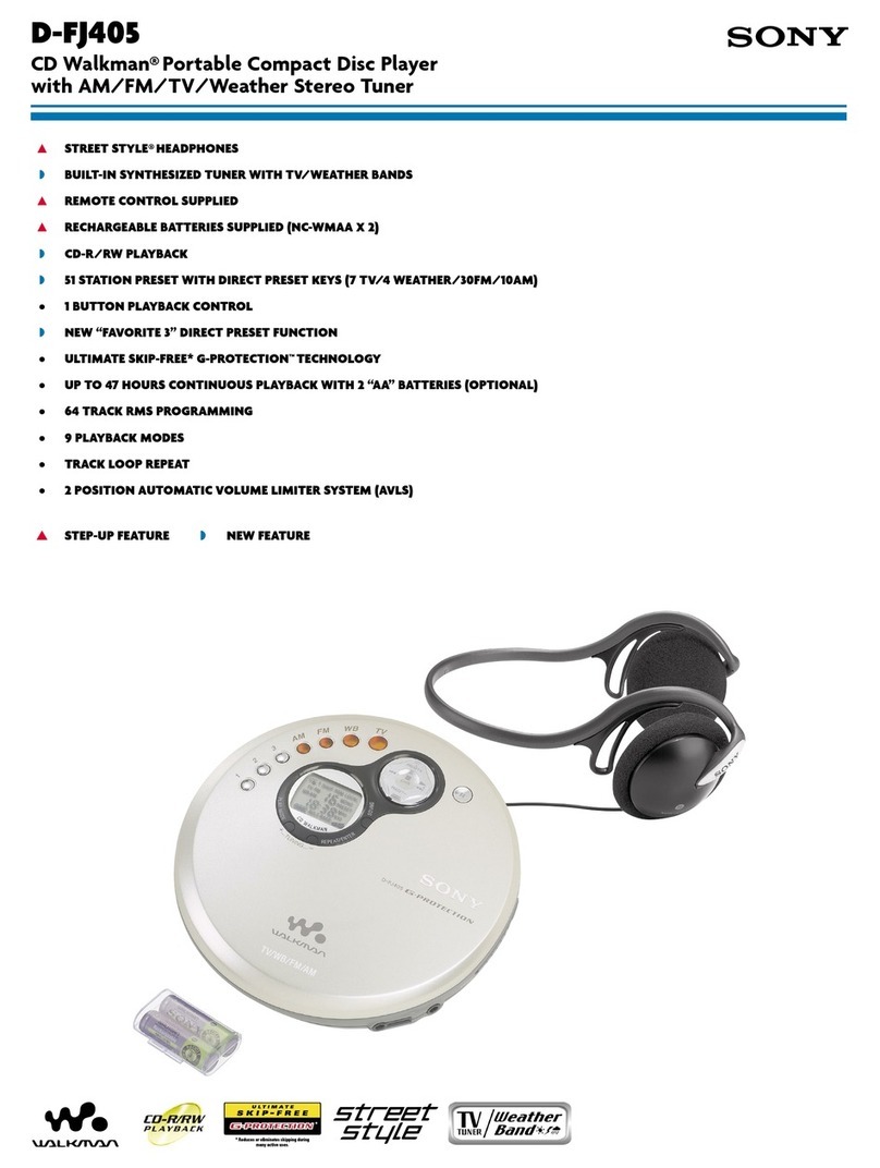
Sony MDP-440 MDP-640D User manual

Sony

Sony MDP-440 MDP-640D User manual

Sony CFD-V35 - Cd Radio Cassette-corder User manual
Sony

Sony CFD-V35 - Cd Radio Cassette-corder User manual

Sony CD Walkman D-E660 User manual

Sony

Sony CD Walkman D-E660 User manual

Sony CDP-590 User manual

Sony

Sony CDP-590 User manual

Sony HCD-V5500 User manual

Sony

Sony HCD-V5500 User manual

Sony Walkman D-NE511 User manual

Sony

Sony Walkman D-NE511 User manual

Sony D-NE518CK - Portable Cd Player User manual

Sony

Sony D-NE518CK - Portable Cd Player User manual

Sony MZ-N707 OpenMG Jukebox NOTES on installing &... User manual

Sony

Sony MZ-N707 OpenMG Jukebox NOTES on installing &... User manual

Sony Walkman D-FJ003 User manual

Sony

Sony Walkman D-FJ003 User manual

Sony CFD-K10 User manual

Sony

Sony CFD-K10 User manual

Sony CDP-CX681 - 200 Disc Cd Changer User manual

Sony

Sony CDP-CX681 - 200 Disc Cd Changer User manual

Sony CFD-E75 Marketing User manual

Sony

Sony CFD-E75 Marketing User manual

Sony D-NF400 User manual

Sony

Sony D-NF400 User manual

Sony D-FJ787 Marketing User manual

Sony

Sony D-FJ787 Marketing User manual

Sony CDX-602 - Compact Disc Changer User manual

Sony

Sony CDX-602 - Compact Disc Changer User manual

Sony DVP-FX810 User manual

Sony

Sony DVP-FX810 User manual

Sony CDX-3500 User manual

Sony

Sony CDX-3500 User manual

Sony Walkman D-EJ101CK User manual

Sony

Sony Walkman D-EJ101CK User manual

Sony CDX-1300 - Fm/am Compact Disc Player Product guide

Sony

Sony CDX-1300 - Fm/am Compact Disc Player Product guide

Sony D-FJ210 - CD Walkman Player User manual

Sony

Sony D-FJ210 - CD Walkman Player User manual

Sony CDP-M7 User manual

Sony

Sony CDP-M7 User manual

Sony CDX-F7705X Operating Instructions  (English Product guide

Sony

Sony CDX-F7705X Operating Instructions (English Product guide

Popular CD Player manuals by other brands

Arcam CD23 Handbook

Arcam

Arcam CD23 Handbook

Sanyo MCD-Z1F Service manual

Sanyo

Sanyo MCD-Z1F Service manual

JVC RC-ST3SL instructions

JVC

JVC RC-ST3SL instructions

Technics SL-P9066 operating instructions

Technics

Technics SL-P9066 operating instructions

Marantz HD-CD1 quick start guide

Marantz

Marantz HD-CD1 quick start guide

Philips AZ1140 Instrukcja obs?ugi

Philips

Philips AZ1140 Instrukcja obs?ugi

Alpine 7909 owner's manual

Alpine

Alpine 7909 owner's manual

JVC CH-X350 instructions

JVC

JVC CH-X350 instructions

RCA RP-7923 instruction manual

RCA

RCA RP-7923 instruction manual

Pioneer DEH-P3550MP XM Operation manual

Pioneer

Pioneer DEH-P3550MP XM Operation manual

Philips Shockproof AX2102 brochure

Philips

Philips Shockproof AX2102 brochure

Philips CD582 user manual

Philips

Philips CD582 user manual

Philips AZ 6821 operating manual

Philips

Philips AZ 6821 operating manual

Lasonic MSU-2020 user manual

Lasonic

Lasonic MSU-2020 user manual

Denon DCD-1420 Service manual

Denon

Denon DCD-1420 Service manual

Panasonic SJ-MR100 operating instructions

Panasonic

Panasonic SJ-MR100 operating instructions

Onkyo DX-7210 instruction manual

Onkyo

Onkyo DX-7210 instruction manual

Cambridge Audio SONATA CD30 manual 

Cambridge Audio

Cambridge Audio SONATA CD30 manual 

manuals.online logo
manuals.online logoBrands
  • About & Mission
  • Contact us
  • Privacy Policy
  • Terms and Conditions

Copyright 2025 Manuals.Online. All Rights Reserved.

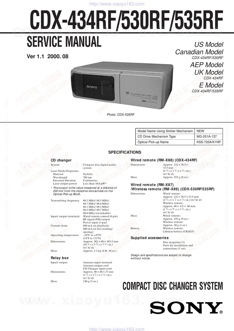
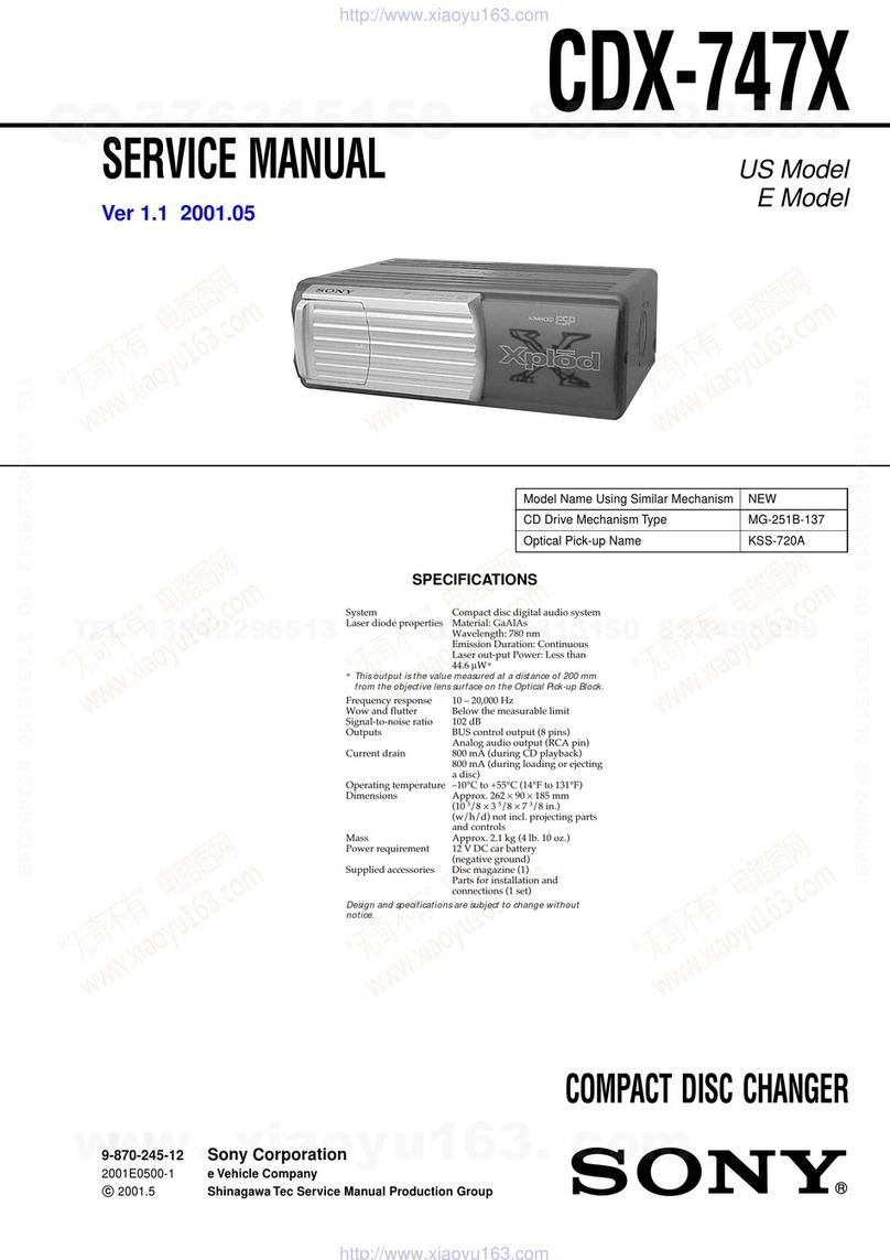
CDP-C320M/C422M
SERVICEMANUAL
UK
Model
E
Model
Australian
Model
i
§
DISC
AUTOMATIC
Disc
LOADING
SYSTEM
B
ef
Photo:
CDP-C325M
CDP-C225/C325
BU-5BD8B
SPECIFICATIONS
General
Power
requirements
UK,
Australian
model:
240
V
AC,
50/60
Hz
AEP,
East
European
model:
220—230
V
AC,
50/60
Hz
E
model:
110
—
120
or
220
—
240
V
AC
adjustable,
50/60
Hz
Power
12
W
consumption
Dimensions
Approx.
355
x
120
x
385
mm
(w/h/d)
(not
including
(14
x
4%
x
15%
inches)
projecting
parts
and
controls)
Approx.
5.0
kg
(11
Ibs
01
02)
fC
P-C325M
CDP-C422M
Compact
disc
digital
audio
system
Laser
Semiconductor
laser
(A
=
780
nm)
Emission
duration:
continuous
Laser
output
Max.
44.6
»W*
*
This
output
is
the-value
measured
at
a
distance
of
about
200
mm
from
the
objective
lens
surface
on
the
Optical
Pick-up
Block.
Frequency
2
Hz
—
20
kHz
(+0.5
dB)
response
Signal
to
noise
More
than
100
dB
ratio
More
than
98
d8
Harmonic
Less
than
0.005%
(1
kHz)
distortion
Channel
More
than
100
dB
(1
kHz)
separation
Wow
and
flutter
|
Below
measurable
limit
Outputs
Output
level
2
V
(at
50
kilohms)
LINE
OUT
Load
impedance
over
10
kilohms
(phono
jacks)
Supplied
accessories
|
CD
P-C825M
CDP-C422M
Audio
signal
1
connecting
cord
|
(phono
plug
x
2
«+
phono
plug
x
2)
Remote
commander
Sony
SUM-3
(NS)
batteries
Design
and
specifications
subject
to
change
without
COMPACT
DISC.
PLAYER
SON
Y.
HEADPHONES
|
Output
level
(stereo
phone
0
—
10
mW
jack)
(variable)
(at
32
ohms)
CDP-C325M/C422M
|
For
the
United
Kingdom
and
European
Countries.
This
Compact
Disc
player
is
classified
as
a
CLASS
1
LASER
product.
The
CLASS
1
LASER
PRODUCT
label
is
located
on
the
rear
exterior.
NOTES
ON
HANDLING
THE
OPTICAL
PICK-UP
The
laser
diode
in
the
optical
pick-up
block
may
suffer
electrostatic
breakdown
because
of
the
potential
di-
ference
generated
by
the
charged
electrostatic
load,
etc.
on
clothing
and
the
human
body.
During
repair,
pay
attention
to
electrostatic
break-
down
and
also
use
the
procedure
in
the
printed
matter
which
is
included
in
the
repair
parts.
The
flexible
board
is
easily
damaged
and
should
be
handled
with
care.
CLASS
1
LASER
PRODUCT
LUOKAN
1
LASERLAITE
KLASS
1
LASERAPPARAT
NOTES
ON
LASER
DIODE
EMISSION
CHECK
The
laser
beam
on
this
model
is
concentrated
so as
to
be
focused
on
the
disc
reflective
surface
by
the
objec-
tive
lens
in
the
optical
pick-up
block.
Therefore,
when
checking
the
laser
diode
emission,
observe
from
more
than
30cm
away
from
the
objective
lens.
SAFETY-RELATED
COMPONENT
WARNING!!
COMPONENTS
IDENTIFIED
BY
MARK
A
OR
DOTTED
LINE
WITH
MARK
A
ON
THE
SCHEMATIC
DIAGRAMS
AND
IN
THE
PARTS
LIST
ARE
CRITICAL
TO
SAFE
OPERATION.
REPLACE
THESE
COMPONENTS
WITH
SONY
PARTS
WHOSE
PART
NUMBERS
APPEAR
AS
SHOWN
IN
THIS
MANUAL
OR
IN
SUPPLEMENTS
PUB-
LISHED
BY
SONY.
Note
on
the
Transit
Key
The
transit
key
on
the
bottom
exterior
of
the
unit
protects
the
optical
system
against
shock
during
transportation.
Before
operating
the
CD
player,
be
sure
to
remove
the
key
by
following
the
instructions
on
the
label,
and
store
it
in
a
safe
place.
When
transporting
the
unit,
replace
the
key
in
its
original
hole
and
lock
it
in
place.
MODEL
IDENTIFICATION
—
Specification
Label
—
CDP-C325M
CDP-C422M
SONY:
COMPACT
DISC
PLAYER
MODEL
No.
AEP,
EE
model:
AC:
220—230V~50/60Hz
UK,
AUS
model:
AC:
240V~50/60Hz
E
model:
AC:
110—120,
220—240V~50/60Hz
12W
@
AUS:
Australian
model
EE
:
East
European
model
|
CDP-C325M/C422M
PROTECTION
OF
EYES
FROM
LASER
BEAM
DURING
SERVICING
This
set
employs
a
laser.
Therefore,
be
sure
to
follow
1.
Laser
Diode
Properties
carefully
the
instructions
below
when
servicing.
Material’.
GaAlAs
Wavelength:
780
nm
Emission
Duration:
continuous
Laser
Output
Power:
less
than
44.6
uW*
*
This
output
is
the
value
measured
at
a
distance
of
ce
:
200
mm
from
the
objective
lens
surface
on
the
of
procedures
other
than
those
specified
herein
Optical
Pick-up
Block.
may
result
in
hazardous
radiation
exposure.
CAUTION
Use
of
controls
or
adjustments
or
performance
2.
During
service,
do
not
take
the
Optical
Pick-up
Block
apart,
and
do
not
adjust
the
APC
circuit.
If
there
isa
breakdown
in
the
APC
circuit
(including
laser
diode),
replace
the
entire
Optical
Pick-up
Block
(including
APC
board).
A
a
II
tat
A
Mad
tA
tt
ta
a
a
NN
St
0
IN
SO
BE
A
mt
PN
DEA
A
at
\
08
RYN
Yt
A
BESKYTTELSE
AF
@JNE
MOD
LASERSTRALING
UNDER
SERVICE
I
dette
apparat
anvendes
laserlys.
Derfor
skal
1.
Laser-didoe
data
nedenstaende
instruktioner
neje
folges
under
service.
@
Materiale:
GaAlAs
@
Belgelangde:
780
nm
Folg
iovrigt
instruktionerne
i
servicemanualen.
@®
Udstraling:
Kontinuerlig
@
Laseroutput:
Max.
0,4
mW*
*
Malt
i
1,6
mm
afstand
fra
overfladen
af
objektiv-
‘ADVARSEL!!
linsen
pa
den
optiske
pick-up
enhed.
Under
service
ma
gjnene
ikke
komme
ner
objektiv-linsen
@
Klassifikation:
Klasse
Ib.
pa
den
optiske
pick-up
enhed.
|
tilfeelde
af
at
det
er
ngdvendigt
at
kontrollere
udsendelsen
af
laserlys,
skal
det
ske
i
en
afstand
af
mere
end
25cm
fra
den
optiske
pick-up.
2.
Adskil
aldrig
den
optiske
pick-up
enhed
under
service,
og
juster
ikke
APC
kredslobet
(Automatic
Power
Control).
Hvis
APC
kredslobet
(incl.
laser-
dioden)
bryder
ned,
skal
hele
den
optiske
pick-up
enhed
(incl.
APC
printkortet)
udskiftes.
LASER
ADVARSEL
MAERKNING
Folgende
mzerkning
findes
indvendig
i
apparatet:
1.
Advarsel
Mzerkning
CAUTION)
«<
INVISIBLE
LASER
RADIATION
WHEN
OPEN
AND
INTERLOCKS
DEFEATED
AVOID
EXPOSURE
TO
BEAM.
ea
Re
ADVARSEL
<
usvNitG
LASERSTRALING
VEO
ABNING
NAR
SIKKERHEDSAFBRYDERE
ER
UDE
AF
FUNKTION
UNDOGA
UDSATTELSE
FOR
STRALING.
VAROITUS:
Laite
sisaltaa,
laserdiodin,
joka
lahettaa
(nakymatonta)
silmille
vaarallista
lasersateilya.
CDP-C325M/C422M
|
SECTION
1
GENERAL
This
section
is
extracted
from
1-1.
LOCATION
AND
CONTROLS
instruction
manual.
Front
Panel
Refer
to
the
pages
indicated
in
( )
for
details.
[1]
POWER
switch
(page
18)
[2]
PLAY
MODE
buttons
CONTINUE
button
(page
18)
SHUFFLE
button
(page
28)
PROGRAM
button
(page
30)
[3]
DISC
1-5
buttons
(page
18)
[4
]
(play)
button
(page
18)
[5
}
Il
(pause)
button
(page
18)
[6
|
@
(stop)
button
(page
18)
I<</PPI
(AMS*)
buttons
(page
24)
</>
(manual
search)
buttons
(page
26)
[9
]
DISC
SKIP
button
(page
18)
=
OPEN/CLOSE
button
(page
18)
[11]
FADER
button
(page
44)
EDIT/TIME
FADE
button
(page
36)
CLEAR
(program
clear)
button
(page
34)
CHECK
(program
check)
button
(page
34)
[15]
TIME
button
(page
22)
Disc
tray
(page
18)
Display
window
PEAK
SEARCH
button
(page
48)
MUSIC
SCAN
button
(page
42)
Remote
sensor
(CDP-C325M
only)
[21]
REPEAT
button
(page
42)
[22]
TIMER
switch
(CDP-C325M
only)
(page
50)
[23]
PHONE
LEVEL
control
(CDP-C325M
Only)
(page
18)
HEADPHONES
jack
(CDP-C325M
only)
*
AMS
is
the
abbreviation
of
Automatic
Music
Sensor.
Remote
Commander
Refer
to
the
pages
indicated
in
(
)
for
details.
CDP-C325M
only
[1]
PROGRAM
button
(page
30)
[2
]
DISC
SKIP
button
(page
18)
[3]
>10
(over
10)
button
(page
24)
[4
]
REPEAT
button
(page
42)
[5
|
™
(stop)
button
(page
18)
[6
|
MUSIC
SCAN
button
(page
42)
FADER
button
(page
44)
<<
>>
(manual
search)
buttons
(page
26)
[9
]
<4
mht
(AMS)
buttons
(page
24)
b>
(play)
button
(page
18)
Il
(pause)
button
(page
18)
[11]
Numeric
buttons
(1-10)
(page
24)
[13]
DISC
1-5
buttons
(page
18)
CONTINUE
button
(page
18)
[15]
SHUFFLE
button
(page
28)
SECTION
2
ELECTRICAL
BLOCK
CHECKING
Note:
1.
CD
Block
basically
constructed
to
operate
without
adjus-
tment.
Therefore,
check
each
item
in
order
given.
2.
Use
YEDS-18
disc
(3-702-101-01)
unless
otherwise
indicat-
ed.
3.
Use
the
oscilloscope
with
more
than
10MQ
impedance.
4.
Clean
an
object
lens
by
an
applicator
with
neutral
deter-
gent
when
the
signal
level
is
low
than
specified
value
with
the
following
checks.
S
Curve
Check
oscilloscope
BD
board
C)
ti
TP(FEO)
Om
—
0+
TP(VC)
O=u-——O
-
Procedure
:
1.
Connect
oscilloscope
to
test
point
TP
(FEO)
on
BD
board.
2.
Connect
between
test
point
TP
(FES)
and
TP
(VC)
by
lead
wire.
3.
Turned
Power
switch
on
and
actuate
the
focus
serch.
(actuate
the
focus
serch
when
disc
table
is
moving
in
and
out.)
4.
Check
the
oscilloscope
waveform
(S
curve)
is
symmetri-
cal
between
A
and
B.
And
confirm
peak
to
peak
level
within
3+1Vp-p.
S
curve
waveform
symmetry
within
3
£1Vp-p
5.
After
check,
remove
the
lead
wire
connected
in
step
2.
Note:
©
Try
to
mesure
several
times
to
make
sure
that
the
ratio
of
A:
B
or
B:
A
is
more
than
10:
7.
e
Take
sweep
time
as
long
as
possible
and
light
up
the
brightness
to
obtain
best
waveform.
RF
Level
Check
oscilloscope
BD
board
()
’
eaten’
TP(RFO)
Ot
OF
TP(VC)
O=t—
0
-
Procedure
:
1.
Connect
oscilloscope
to
test
point
TP
(RFO)
on
BD
board.
2.
Turn
Power
switch
on.
3.
Put
disc
(YEDS-18)
in
and
playback.
4,
Confirm
that
oscilloscope
waveform
is
clear
and
check
RF
signal
level
is
correct
or
not.
Note:
Clear
RF
signal
waveform
means
that
the
shape
“©”
can
be
clearly
distinguished
at
the
center
of
the
waveform.
VOLT/DIV:
200mvV
TIME/DIV:
500nS
RF
signal
waveform
WX
\
i)
f
WY
NY
Haaaue
A
\ i
AA)
ay
Tf
A)
V
level
:
|
1.2
203
Vp-p
oscilloscope
BD
board
C)
mmc,
TP(TEO)
Owg—toy
TP(VC)
gGeg—lo
-
ANY
()
X)
WM
E-F
Balance
Check
Procedure
:
1.
Connect
test
point
TP
(ADJ)
to
ground
and
TP
(TES)
to
TP
(VC)
with
lead
wire.
2.
Connect
oscilloscope
to
test
point
TP
(TEO)
on
BD
board.
3.
Turn
Power
switch
on.
4.
Put
disc
(YEDS-18)
in
and
playback.
5.
Confirm
that
the
osilloscope
waveform
is
symmetrical
on
the
top
and
bottom
in
relation
to
0V,
and
check
this
level.
Traverse
oscilloscope
symmetry
level:
2£1Vp-p
6.
Remove
the
lead
wire
connected
in
step
1.
RF
PLL
Free-run
Frequency
Check
Procedure:
1.
Connect
frequency
counter
to
test
point
(PCK)
with
lead
wire.
frequency
counter
Main
board
ki
:
TP(PCK)
Ot
10+
tr
Confirm
that
reading
on
frequency
counter
is
4.3218MHz.
Turn
Power
switch
on.
Focus/Tracking
Gain
This
gain
has
a
margin,
so
even
if
it
is
slightly
off.
There
is
no
problem.
Therefore,
do
not
perform,
this
adjustment.
Please
note
that
it
should
be
fixed
to
mechanical
center
position
when
you
moved
and
do
not
know
original
position.
Adjustment
Locations
:
(BD
Board)
—Conductor
Side—
{MAIN
Board}
—Component
Side—
SECTION
3
DIAGRAMS
3-1.
CIRCUIT
BOARDS
LOCATION
BD
BOARD
LOADING
MOTOR
BOARD
POWER
SW
BOARD
OPEN/UP
SW
BOARD
SW
BOARD
DISPLAY
BOARD
3-2.
SEMICONDUCTOR
LEAD
LAYOUTS
BA6297AFP
CXD25019
LA5602
M5293L
2SA1175-HFE
letter
side
12345
(TOP
VIEW)
pc*F
CXA1291P
CXD2560M
M5F7807L
DTA114ES
DTC114ES
6
4
1
38
DTC144ES
I
3
6
8
(TOP
VIEW)
(TOPVIEW)
E
CxXD2500AQ
CXD2561BM
M5218AP
SBX1610-59
“8
CXP50116-2879Q
CASE
7
6:5
CXP50120-0200
i
i
i
i
GU
UU
1
od
me
(TOP
VIEW)
CHORE)
i
2?
1]=Voo
2=SIRCS
3=GND
TABLE
MOTOR
BOARD
MAIN
BOARD
GP-1A521
11ES2
1N4148M
RD8.2ES-B2
cathode
anode
©
IC
Block
Diagrams
1¢301
CXD2500AQ
IC101
CXD2501Q
0]
1]
>
oO
az
O@
IC202
LA5602
EN
ES
Ww
a
oa
ao
Zz
aa
Ww
aa
Qa
>
>oagaunno
Lt
aagazu2zn
Zz
bh
CNEDENEDENESENED
(S)
IGEN
SHAPER
TFDR
and
NC
PWM
MOOULATOR
(45)
TEST
MIRA/
NC
DFCTY JUMP?
FOK
SEACH
DETECTOR
CONTROL
SRDR
#-COM
INTERFACE
SOUT
OIRC
ASYMMETRY
CORRECTOR
REF
ERENCE
VOL
TAGE
IC306
LA9215
VARIABLE
PITCH
CONTROL
DIGITAL
AUOIO
INTERFACE,
ADRESS
GENERATOR
AMP
REFERENCE
VOLTAGE
(7)
V
OUT
OVER
CURRENT
LIMITTER
RESET
cen
|
OVER
HEAT
(5)
PROTECTION
ON/OFF
7
ay
m
(,)
$s8so
SCOR
WFCK
(61)
EMPH
oouT
MD2
C16M
C4M
FSTT
XTSL
XTAO
vss
APTL
APTR
DAQ1
DA02
DA03
DAOSL
DAOS
OA06
DA07
OA08
DAO?
CDP-C325M/C422M
CDP-C325M/C422M
CDP-C325M/C422M
CDP-C325M/C422M
|
_
CDP-C325M/C422M
CDP-C325M/C422M
e
Semiconductor
Location
3-3.
PRINTED
WIRING
BOARDS
e
Refer
to
page
7
for
Semiconductor
Lead
Layouts.
[
RefNo.
|
Location
felee
ea
a
I
ee
Oe
Se
es
Oe
es
Oe
OO
I
Se
ee
ee
ee
29
34
A
{BD
BOARD
}
B
(MAIN
BOARD}
(CHASSIS)
OPTICAL
Pigg
4
PICK-UP
BLOCK
(KSS
240A)
|
C
/
seo!
!
SELECTOR]
a
a
10
~-120V
pos
|
[SW
BOARD}
:
y
CL
I
a
CD
Natl
ie
La
220-240V
[
NS
l
D
#
ss
.
ae
l
|
Eb
r
ome
A
1
|
SW72
|
SW7I9
SW718
SW716
SNe
SW7l2
SW7II
SW7l0
SW709
SW708
SW707
No
&
OPEN/
41a
I
|
Cost
[ow]
ise
THE
Sad
peerelstaeaieisteleel|
[i2]
EF
yee
POWER
CECE
EEE
ECE
i
baseeaceiese
_
TRANSFORMER
=
:
AC
se
IN
FL60I
FLUORESCENT
INDICATOR
TUBE
Sie
E
LOADING
Note:
F
:
:
|
MOTOR
BOARD
@®
oO——§:
parts
extracted
from
the
component
side.
i
e
@
=:
Through
hoie.
|
:
e
:
:
Pattern
on
the
side
which
is
seen.
|
®
:
Pattern
of
the
rear
sice.
i
ms
CN502
Gye
MOTOR
M70:
SHUFFLE
é
Au
BUS
LOADING
PROGRAM
=
f
REPEAT
1
=
‘Aa
:
iii
|
|
|
wm
Recs
I-6
38-7305
3751
RV751
PHONE
LEVEL
i=
>|
fee
1
Lz
om
=
i
a
Ra
RR
RS
|
eh
mt
f
.
{
f
|
i
Shock
ee
Las
HHH
SEE
sanaaaaeanaaial
|
©6325
_i(e)
coo
inal
1-643-530-
|
[11]
arora)
i
Coro
VOU
BN
0 0
0
2000
7
ma
Sg
a]
i
L
—10—
—11—
|
—12—
,
—13—
|
a
3-4.
SCHEMATIC
DIAGRAM
e
Refer
to
page
8
for
IC
Block
Diagrams.
1
2 3
4
5
6
7
8 9
10
11
12
13
14
15
16
17
18
19
21
e
Waveforms
N
©
(DISPLAY
BOARD]
Se
Seen
eye
ee
a
eee
a
ee
a
ll
et
|
sweos
es
[BD
BOARD
]
1C101
re
102
;
C601
Mmmaned
ae
ifsiees
FOCUS/
TRACKING
REMOCON
|
FOCUS/TRACKING,
J
COIL
DRIVE,
+
$Bx1610-59(
=
SLED
SERVO.
‘
SLED/SPINDLE
BELECTOR
|
pLay
<
aA
C325M
EFM
COMPARATOR
TP
[TES
MOTOR
DRIVE
TP
ve
FL601
FLUORESCENT
INDICATOR
TUBE
£106
1.08
2
vot
ALL
JUST
EDIT
1
DISCS
LINK-A-B
|
[2-0]
Sw604
SW605
Sw6é08
SWwé07
SW606
f
EDIT/
<
ra)
Q
2
999?
999999
2
4
QO
rad
R/KIAIO
w
AION)
gZ
HU
Ato
SHUFFLE
PROGRAM
CN603
0.47
usec
iclol_
(@)
PLAY
(TES)
ic301
(6)
REPEAT
1
i
oO
wm
0
=
199999
96
9
9 9
9
OD
So
PN
ENS
A
Fee
Sm
ovo
(2)
a
lee)
Op
F
et
Sol
Aiea
a
ene
eat
Ss
e
12P
-
Lo
KI
|
4-40-33
a
loz
I
'co
PL
|
eno
<a
lg
(SPINDLE)
1200
4521
03FP
Ho}
K?
<
os
5
Ks
:
3
ii
|
BARRRERRERRRRRARRRRRRRRRRARAAT
FL
A
iE
Sat
aR
m2
=
Tordele)
CN6OI
=
ICIOl
PLAY
(FES)
=
\
eg)
FRERERETRERE
SERA
RREPRELREERELE
REE
EEE
—————————
Oo
9
Osbeneaa
@
an
A
Tyee)
eo
es
BIB!
epaceg
ily
os
(SLED)
OPTICAL
PICK-UP
BLOCK
=
i
Fa
(KSS-240A)
a7
—
-
_
wy]
sw7ol
CN701
ies
ere
|
_
ie
_
iS
fever
Pry
cyst
(SW
BOARD}
c703
“|
9P
0
aaa
a
[
|sw
(8
O
O
é
*
|
CA
i]
ee
—
=|
-2
ie
oi
18]
sy
I
ry
TKo
J
10301
@)
PLAY
(MDP)
=
ae
R7i6
R714
R713
RT
12
pop
jon
a
[pores
SW
18k
68K
3.9K
po]
—
BOARD
ps
ea
ep
=
i
sw72l
SW7I9.sSW7I8.
SW7IT_‘SW7I6
DOPEN/
—
[>]
[s¢]
[Kes]
I
rs
R75
RI
Rio
|
R709
Bk 9K
2.7k
r
|
d
d
d b
&
R701
pd
R703
pd
R704
7b
1
ge
ge
ge
ge
ge
Ber
ge
Be
de
Sty
am
t
i
i t ;
Note:
SW720
SWw715
SW714
SW71I3
SW707
Sw708
SW709
SWT7I0
a‘
2
‘
.
S
ph”
ect
[SiR
+
nce
©
All
capacitors
are
in
uF
unless
otherwise
noted.
pF:
uuF
Gag
ee
ie
See
=
te
ge
ae
=
SKIP
5OWV
or
less
are
not
indicated
except
for
electrolytics
$702
|
TABLE
MOTOR
OPEN/UP
|
crtirur
|
LOADING
MOTOR
R702
|
R705
|
R706
|
ROT
|
and
tantalums.
°
UP+OPEN
:
'
BOARD
SW
BOARD
:
|
BOARD
18k
6-8k
3.9k 2.7k
CRr708
no
e
All
resistors
are
in
2
and
%,W
or
less
unless
otherwise
I
J
1
do
de
alc
de
de
de
am
ale
specified.
rr
|
Sw702
$w703.-SW704.
Ss
SW705.-
SW706.—
SW7Ii_—
SW7I2
Pat
|
pisc4]
[discs]
[Music]
|
PEAK
Note:
The
components
identified
by
mark
A
or
dotted
(G3)
SCAN
|
(SEARCH
line
with
mark
A
are
critical
for
safety.
Ve
sigighi
PRRPASMERP
REE OSE
Aeaae
ete
ene
Replace
only
with
part
number
specified.
CN707
a
|>
SRIAD
2
valle)
satis
8
-
1
5P
=
-
-
_
es
oo]
ro)
Sacuem
:
B-
Line
\_
1s)
zp
:CD
A705
=
asl
TOLL
LLLLL
LLL
LLL
LLL
owe
(PEEL
LEL
LLL
ee
=
CETERA
ea
Se
te
eof
RLEX
pbb
Loh
oh
oh
oh hh
lath
hd
oh
pepe
dent
FLE
pitied
FLEX
4
=
=
FLEX
®
Voltage
and
waveforms
are
dc
with
respect
to
ground
under
GCOOSOOCOODOO0CCSECCGG
Lo?
9
>?
of
=
-
Ciixion
aX eX 7X
eX
SAX
3X21)
4
209990990999
9099
99933303
039353330
|
CC
err
east
as
ee
ie
a
:
.
5
SSS
SERA
SAG
UA
See
no-signal
conditions.
4
van
3
LE
|
San
en
pranc-aumtocrange
gor
oer
es
SSS
SS
ee
-
ve
aeegedd
z2°5
8&8
yy
YS
cS
YY
|
ee
eee
ee
ce
eee
caaaana
©
Voltages
are
taken
with
a
VOM
Unput
Imnped
10M)
SSGzeegeE
SSSR
Stgzs
ae:
°
ca
i
ky
RO
ecee.
ss
or
yore
eeevy
yy
yy
ae
i
aes
eG
BR
y,
Voltage
variations
may
be
noted
due
to
normal
produc-
o—
TT
oe]
fox
te]<)
Re
Pa.
age
CHT
He
tion
tolerances.
c408
ESS
NEL
SME
Ge]
onto}
MUTING,
ATT
|
©
Waveforms
are
taken
with
a
oscilloscope.
|
z
D/A
CONVERTER
SV]
J751
Voltage
variations
may
be
noted
due
to
normal
produc-
Sesoeos
cae
a
[HeaoeHones
|
§
|§s
UESOb
EASEIS
jose
HEAORHONES
tion
tolerances.
40!
:
—3|
“26
~3i.
-26.9
=26.9
-223
-8.6
~4.1
[
Tt
]
3
|gg
®
Circled
numbers
refer
to
waveforms.
TC
i
——
LLC
anil
3
|e
FINALL
LEAN
|
eae
ae
8
ie
©
Signal
path.
és
KiKisKi
IGN
SKAKISKIZKI
OX
9X8
X7XEXSKAKS2KI)
aapT
ply
plete
Tek
are
ees
rsa
as
pie
ee
NA
|
—
26.9
a
“10
-8.5
26
4
SYSTEM
ra.
|
R563
56
"|
_
Raye
ogee
C325M
I
07
TBLR
PHONE
AMP
AVOD
¢}
Cate
:
R383
1k
-2
€359\22000,
S
:
no)
(eyo
2gSS
39k
|
Was
=>)
(R}
sis
ai
er
(oe
mee
2
aed
J501
LINE
OUT
ats
Aas
887
39k]
ta
8
gis
aT:
AYSSR
o
0.0015
6)
a
=
i
A2.6,
L309)
LR
-I
L
Sy
XVOO
Ri
(+)
y
Ler-Teh|
mis
ee)
aid
pie
GaPsss
39K}
OH]
R384
Ik
©
CXPSONG
(C325M)
CXP50120
(C422M)
FL
DRIVE/SYSTEM
CONTROL
10302
CX2560M
C392
0.1
RST
R368 C366
305
56k
39p
OpH
C350
$7
C349
=
/
10303
ley
220000
CX825616M
L301
DIGITAL
FILTER
f
On
Q304
Q305
9302
aa04
AMP
+B
INVERTER
AMP—B
2841348
=.
SWITCH
SWITCH
TABLE/
LOADING
MOTOR
DRIVE
TIMERSW
TBLSENSOR
C385
47»
14V
Yio.4
0305
9302
25a1
368
"ll
Woo
eeoe
C422M
4
D401
CNSO2
[AU
BUS]
R440
Ik
IN4148M
SP
(1)
Au
BUS
J
Leg)
e
GND
R442
10k
had
BAIA4N-TP
aa
ie
(es
cil
|
BUFFER
RSI
|
10
pe
pare
|
jAMP
tB
SWITCHING
~~
0207
0208
NES2
11ES2
ny
NO
ou
oo
ow
——s
aaa
es
SBSO
++}
s
S
g
Eo
EXCK
=
=
$QS0
(SUBQ)
8
|e
socuk
|
ny
nO
ou
P=T—)
oN
o
RESET
ON/OFF,
+5V
REG
Ls
—32V
REG
-30V>——=
T9201
POWER
TRANSFORMER
f
,
Fs
SENS
Textoh|
Y
$201
A
CNIN
VOLTAGE
—
Cx82500A0
SELECTOR
DIGITAL
SIGNAL
PROCESSOR
XLTO
/CLV
SERVO
+7V
REG
205
9201
|
47y
0203
SOV
2SAVOABTP
1607
°Fa25
5
en
:
C203
2204
:
1000«
16¥)
1
fES2-TAZB
>
C20:
05
R202
5ék
10202
LAS602
ST
2
4
92
-
|
—
MODEL
33008
16v|
11€S2-TA2B
I
eel
EXPECT
~
i
es
ee
E
MODEL
|
MAIN
BOARD
———
Lt
:
=
=
%
NOT
REPLACEABLE
:
BUILT
IN
TRANSFORMER
04
goal
2
ae
==16—
coat
ames
OS