Sony HCD-W550 User manual

HCD-W550
CanadianModel
AEP Model
UKModel
E Model
AustralianModel
TouristModel
SERVICE MANUAL
STEREO CASSETTE DECK CD PLAYER
MICROFILM
CD Model Name Using Similar Mechanism HCD-GR8/RX90
Section CD Mechanism Type CDM38-5BD29A
Base Unit Name BU-5BD29A
Tape deck Model Name Using Similar Mechanism HCD-GR5/RX50
Section TapeTransport MechanismType TCM-220WR2E
Manufactured under license from Dolby Laboratories
Licensing Corporation.
“DOLBY” and the double-D symbol aare trademarks
of Dolby Laboratories Licensing Corporation.
SPECIFICATIONS
• HCD-W550 is the deck, CD section
inMHC-W550/W770AV.
CD player section
system Compact disc and digital
audio system
Laser Semiconductor laser
(l = 780 mm)
Emission duration :
continuous
Laser output Max. 44.6 mW*
*This output is the value
measured at a distance of
200 mm from the
objective lens surface on
the Optical Pick-up Block
with 7 mm aperture.
Frequency response 2Hz - 20 kHz (± 0.5dB)
Wavelenght 780 - 790 mm
Signal to noise ratio More than 90 dB
Dynamic renge More than 90 dB
CD OPTICAL DIGITAL OUT
(Square optical connector jack, rear panel)
Wavelength 600 mm
Output Level - 18 dBm
Tape player section
Recording system 4 track 2 channel stereo
Frequency response 60 - 13,000 Hz (± 3dB),
(DOLBY NR OFF) using Sony TYPE I
cassette
60 - 14,000 Hz (± 3 dB),
using Sony TYPE II
cassette
General
Dimensions (w / h / d)Approx. 280 ¥ 205 ¥ 359
mm
Mass Approx. 4.3 kg
Design and specifications are subject to change without
notice.

— 2 —
TABLE OF CONTENTS
SERVICING NOTE
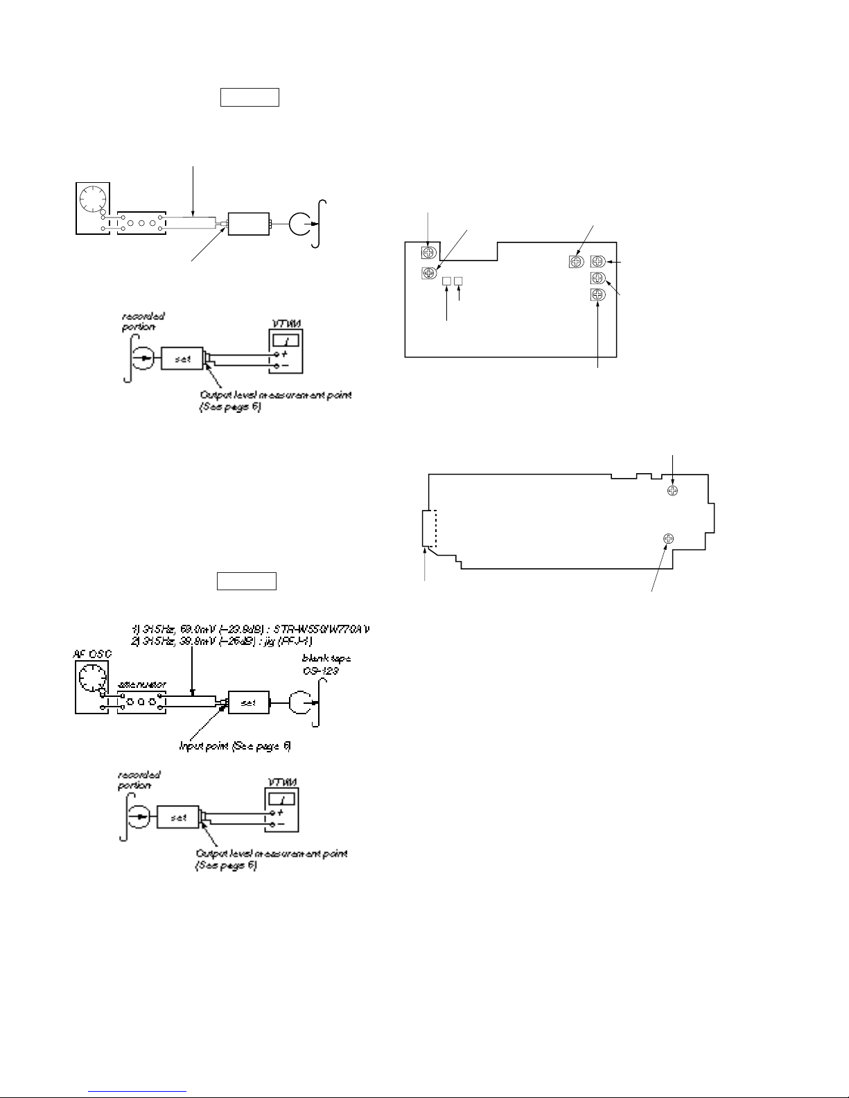
• Supplying power during servicing
This equipment cannot operate without using a separate power supply. Connect to the STR-W550/W770AV when performing service
work.
To apply power set the SYSTEM POWER switch on the Tuner/Amp to ON.
When other units are not available use the PFJ-1 power supply jig.
When using the PFJ-1, simultaneously press the CD STOP button and the DECK A )(fast rightward) button to turn on the power.
[Connection Diagram]
PFJ-1
(Power Supply Jig)
POWER SW
FH-E939,838,737,
MHC-6600,5600,
CDP/TC
Connector Cable 17P
(Supplied with set)
Set
CNB108 17P
SYSTEM CONTROL
Conversion Board
(J-2501-138-A)
1. GENERAL ······································································ 3
2. DISASSEMBLY
2-1. Back Panel, CD Block Removal········································· 4
2-2. Cassette Lid (A)/(B) Assy, Mechanism Deck Removal ···· 4
2-3. Main Board, Resistor Board, Front Panel Assy Removal ·· 5
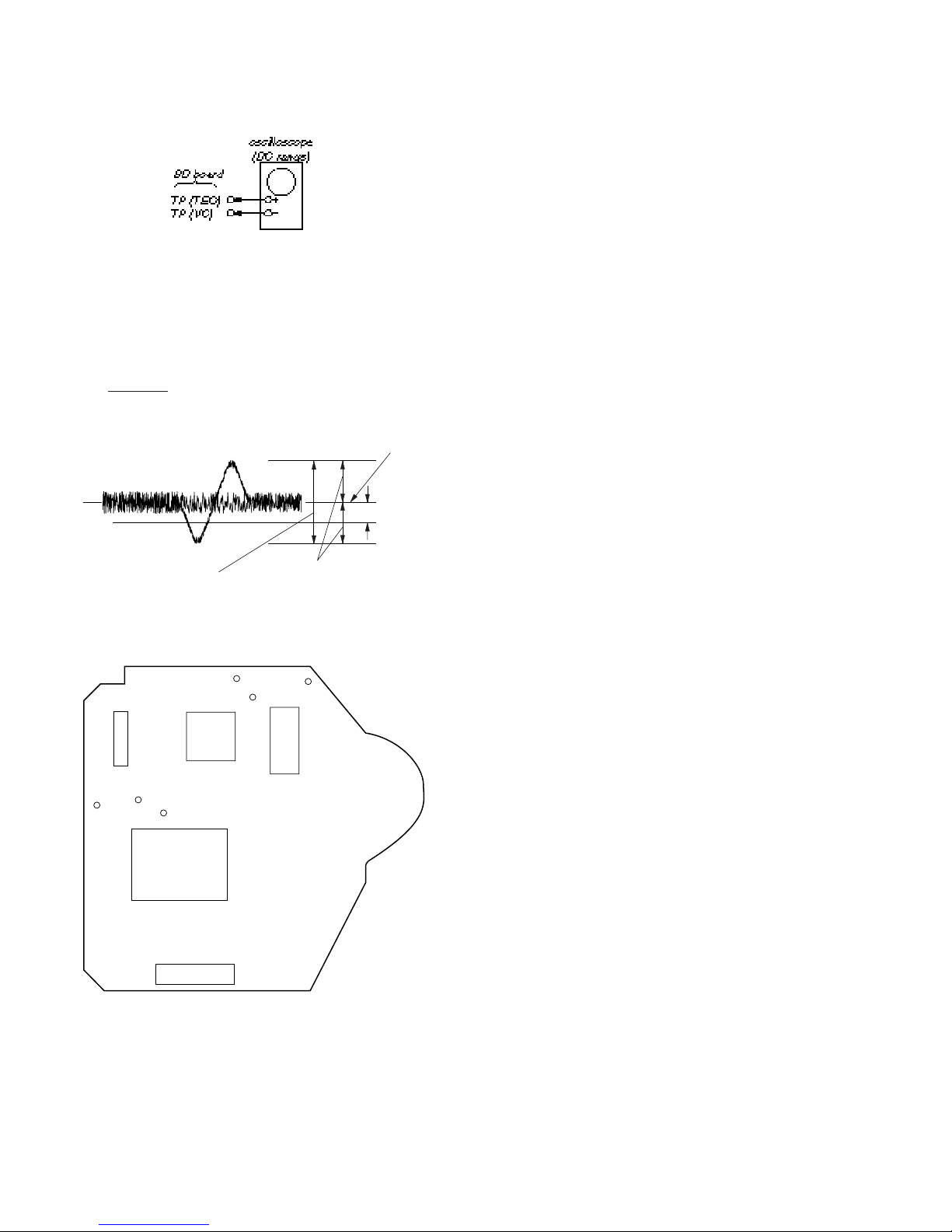
3. ADJUSTMENTS
3-1. Mechanical Adjustment ······················································ 6
3-2. Electrical Adjustment ························································· 6
4. DIAGRAMS
4-1. Block Diagram ································································· 11
4-2. Circuit Boards Location ··················································· 13
4-3. Schematic Diagram — Audio Section —························· 14
4-4. Printed Wiring Board — Audio Section — ······················ 17
4-5. Printed Wiring Board — BD Section — ·························· 19
4-6. Schematic Diagram — BD Section — ····························· 21
4-7. Printed Wiring Board — Motor Section —······················ 23
4-8. Schematic Diagram — Motor Section — ························ 25
4-9. Schematic Diagram — Panel Section — ························· 27
4-10. Printed Wiring Board — Panel Section —······················· 29
4-11. Printed Wiring Board — Main Section — ······················· 32
4-12. Schematic Diagram — Main Section — ··························35
4-13. IC Block Diagrams ···························································38
4-14. IC Pin Function ································································ 40
5. EXPLODED VIEWS
5-1. Main Section····································································· 42
5-2. Front Panel Section ·························································· 43
5-3. CD Mechanism Deck Section-1 (CDM38-5BD29A) ····· 44
5-4. CD Mechanism Deck Section-2 (CDM38-5BD29A) ····· 45
5-5. Base Unit Section (BU-5BD29A) ···································· 46
5-6. Tape Mechanism Deck Section-1 (TCM-220WR2E) ······ 47
5-7. Tape Mechanism Deck Section-2 (TCM-220WR2E) ······ 48
6. ELECTRICAL PARTS LIST ··································· 49

— 3 —
SECTION 1
GENERAL
123 456 7
8
9
!º
!¡
!™
!£
!¢
!∞
!§
!¶
!•
!ª
@º
@¡
@™
@£
@¢
@∞
1DISC SKIP EX-CHANGE Button (CD)
20Button (CD)
3)Button (CD)
4DISC 1 Button (CD)
5DISC 2 Button (CD)
6DISC 3 Button (CD)
76OPEN/CLOSE Button (CD)
8·P Button (CD)
9pButton (CD)
!º ·Button [B] (DECK)
!¡ ªButton [B] (DECK)
!™ πButton [B] (DECK)
!£ )Button [B] (DECK)
!¢ 0Button [B] (DECK)
!∞ DIRECTION MODE Button (DECK)
!§ PAUSE Button (DECK)
!¶ REC Button (DECK)
!• HI-SPEED DUBBING Button (DECK)
!ª CD SYNCHRO Button (DECK)
@º DOLBY NR Button (DECK)
@¡ )Button [A] (DECK)
@™ 0Button [A] (DECK)
@£ πButton [A] (DECK)
@¢ ªButton [A] (DECK)
@∞ ·Button [A] (DECK)

— 4 —
SECTION 2
DISASSEMBLY
Note : Follow the disassembly procedure in the numerical order given.
CASE
Unscrewthefive case attachmentinthe screws(case)
(M3 ×8) ×4, (+BV 3 ×8) ×1 and remove the case.
2-1. BACK PANEL, CD BLOCK REMOVAL
7
Screw
+BVTP 3
×
10
1
Screw
+BVTP 3
×
10
1
Screw
+BVTP 3
×
10
6
Screw
+BVTP 3
×
10
5
CN111 (8 pin)
4
CN112 (9 pin)
3
Flat wire (19 core)
8
CD block
2
Back panel
2-2. CASSETTE LID (A)/(B) ASSY, MECHANISM DECK REMOVAL
1Press the EJECT button and open the cassette lid.
6
Screw
+BVTP 3
×
8
7
Screw
+BVTP 2.6
×
8
4
Flat wire (11 core)
5
Flat wire (21 core)
Mechanism Deck (TCM-220WR2E)
2
8
1
1
3

— 5 —
2-3. MAIN BOARD, RESISTOR BOARD, FRONT PANEL ASSY REMOVAL
3
Screw
+BVTP 3
×
8
2
Front panel assy
6
Screw
+BVTP 3
×
8
1
Screw
+BVTP 3
×
8
4
Bracket (H/S)
5
Resistor board
7
Main boar
d
• Tray (Slide) getting out procedure on the power supply is OFF
Rotate the BU CAM assembly in the direction of the arrow and pull out the slide.
Tray (Slide)
1
BU CAM assy

— 6 —
SECTION 3
ADJUSTMENTS
3-1. MECHANICAL ADJUSTMENT
PRECAUTION
1. Clean the following parts with a denatured-alcohol-moistened
swab:record/playback head pinch roller
erase head rubber belts
capstan idlers
2. Demagnetize the record/playback head with a head
demagnetizer.
3. Do not use a magnetized screwdriver for the adjustments.
4. After the adjustments, apply suitable locking compound to the
parts adjusted.
5. The adjustments should be performed with the rated power
supply voltage unless otherwise noted.
•TorqueMeasurement
• Tape Tension Measurement
3-2. ELECTRICAL ADJUSTMENT
1. The adjustment should be performed in the publication.
(Be sure to make playback adjustment at first.)
2. The adjustmentandmeasurementshould be performed for both
L-CH and R-CH.
• Switch position
DOLBY NR switch : OFF
FUNCTION button : OFF
EFFECT switch : OFF
DBFB switch : OFF
3. Deck section electrical adjustments are made in test mode by
press key switch same time CD STOP DECKASTOP and
DECK B STOP button.
4. Input point and output level measurement point.
• Test Tape
0 dB=0.775V
Record/Playback Head Azimuth Adjustment
DECK A DECK B
Procedure:
1. Forward Playback mode
Reverse Playback mode
Mode Torque Meter Meter Reading
Forward CQ-102C 36 to 61g•cm
(0.50 – 0.84 oz•inch)
Forward CQ-102C 2 to 6g•cm
Back Tension (0.028 – 0.083 oz•inch)
Reverse CQ-102RC 36 to 61g•cm
(0.50 – 0.84 oz•inch)
Reverse CQ-102RC 2 to 6g•cm
Back Tension (0.028 – 0.083 oz•inch)
FF, REW CQ-201B 61 to 143g•cm
(0.85 – 1.99 oz•inch)
Mode Tension Meter Meter Reading
Forward CQ-403A
more than 100 g (3.53 oz)
Reverse CQ-403R
more than 100 g (3.53 oz)
DECK SECTION
Tape Signal Used for
P-4-A100 10 kHz, –10 dB
Head Azimuth Adjustment
P-4-L300 315 Hz, 0dB LevelAdjustment
WS-48B 3 kHz, 0dB Tape Speed Adjustment

— 7 —
2. Turn the adjustment screw for the maximum output levels. If
these levels do not match, turn the adjustment screw until both
of output levels match together within 1 dB.
3. Playback Mode
4. Change the playback mode and repeat the steps 1 to 3.
5. After the adjustment, lock the adjustment screw with suitable
locking compound.
Adjustment Location:
— Record/playback head (Deck A and B) —
Tape Speed Adjustment DECK A DECK B
Note: Start the Tape Speed adjustment as below after setting to the
test mode.
Set to test mode. (Press key switch same time CD STOP
DECK A STOP and DECK B STOP button.)
Test mode off. (Power off.)
Procedure:
• Perform high speed adjustment before normal speed adjustment.
Mode: Playback
* Continue to press HIGH SPEED DUBBING switch (S259) in
playback mode : High speed playback.
Frequency difference between the beginning and the end of the
tape should be within ± 3%.
Frequency difference between deck A and deck B the beginning
of the tape should be within 1.5 %.
Adjustment Location: AUDIO board (See page 8)
Sample Value of Wow and flutter
W.RMS (JIS) within 0.3%
(test tape: WS-48B)
Playback level Adjustment DECK A DECK B
Procedure:
— FWD playback Mode —
Deck A is RV311 (L-CH) and RV411 (R-CH), Deck B is RV301
(L-CH) and RV401 (R-CH) so that adjustment within adjustment
level as follows.
Adjustment Level:
LINE OUT level : –8.2 to –7.2 dB (301.5 to 338.3 mV)
Level Difference between Channels : within 0.5 dB
Confirm the OUTPUT level does not change in playback mode
while changing the mode from playback to stop several times.
Adjustment Location: AUDIO board (See page 8)
Speed
*High
Normal
Deck
A
B
A
B
Adjustment
RV652
RV652
RV651
RV651
Frequency counter
5,910 to 6,090 Hz
2,910 to 3,090 Hz
+
–
VTVM
set
test tape
P-4-L300
(315 Hz, 0 dB)
Output level measurement poin
t
(See page 6)

— 8 —
Record Bias Adjustment DECK B
Procedure:
1. Record mode
2. Mode: Playback
3. Confirm playback the signal recorded in step 1 become
adjustment level as follows.
4. If these levels do not adjustment level, adjustment the RV341
(L-CH) and RV441 (R-CH) to repeat steps 1 and 4.
Adjustment level: Playback output of 315 Hz to playback output
of 10 kHz: 0 ± 1.0 dB (0 ± 4.5mV).
Adjustment Location: AUDIO board
Record Level Adjustment DECK B
Procedure:
1. Record mode
2. Playback mode
3. Confirm playback the signal recorded in step 1 become
adjustment level as follows.
4. If these levels do not adjustment level, adjustment the RV401
(L-CH) and RV451 (R-CH) to repeat steps 1 and 4.
Adjustment Level:
OUTPUT level: –23.8 dB ± 1.0 dB (56.1 to 44.6 mV)
Adjustment Location: MAIN board
Adjustment Location :
[AUDIO BOARD] — Component Side —
[MAIN BOARD] — Component Side —
RV301 : Playback Level (Deck B L-CH)
RV401 : Palyback Level
(Deck B R-CH) RV651 :Tape Speed (Normal)
RV341 : Record Bias (L-CH)
RV441 : Record Bias (R-CH)
RV652 :Tape Speed
(Hight)
RV311 : Playback Level
(Deck A L-CH)
RV411 : Playback Level (Deck A R-CH)
RV451 Record Level (R
)
RV401 Record Level (L)
CNB108
attenuator
set
1) 315 Hz
2) 10 kHz 69.0mV (–23.8dB) : STR-W550/W770AV
38.8mV (–26dB) : jig (PFJ-1)
blank tape
CS-123
AF OSC
Input point (See page 6)

— 9 —
CD SECTION
Note :
1. CD Block is basically designed to operate without adjustment.
Therefore, check each item in order given.
2. UseYEDS-18 disc (3-702-101-01) unless otherwise indicated.
3. Use an oscilloscope with more than 10M impedance.
4. Clean the object lens by an applicator with neutral detergent
when the signal level is low than specified value with the
following checks.
Focus Bias check
Procedure:
1. Connect oscilloscope to test point TP (RF). (GND terminal :
VC)
2. Turned Power switch on.
3. Put disc (YEDS-18) in and playback.
4. Confirm that the shape “ ” can be clearly distinguished at the
center of the waveform and check the RF signal level.
• RF signal
S Curve Check
Procedure:
1. Connect oscilloscope to test point TP (FEO).
2. Connect between test point TP (FOK) and GND by lead wire.
3. Turn Power switch on.
4. Put disc (YEDS-18) in and turned Power switch on again and
actuate the focus search. (actuate the focus search when disc
table is moving in and out.)
5. Check the oscilloscope waveform (S-curve) is symmetrical
betweenAand B. And confirm peak to peak level within 3±1
Vp-p.
S-curvewaveform
6. After check, remove the lead wire connected in step 2.
Note: • Try to measure several times to make sure than the ratio of
A : B or B : A is more than 10 : 7.
• Take sweep time as long as possible and light up the
brightness to obtain best waveform.
RF Level Check
Procedure:
1. Connect oscilloscope to test point TP (RF) on BD board.
2. Turned Power switch on.
3. Put disc (YEDS-18) in and playback.
4. Confirm that oscilloscope waveform is clear and check RF
signal level is correct or not.
Note:
Clear RF signal waveform means that the shape “ ” can be
clearly distinguished at the center of the waveform.
• RF signal

— 10 —
E-F Balance (1 Track Jump) check
(Without remote commander)
Procedure:
1. Connect oscilloscope to test point TP (TEO) on BD board.
2. Turned Power switch on.
3. Put disc (YEDS-18) in to play the number five track.
4. Press the “P(Pause)”button. (Becomesthe 1 track jump mode)
5. Check the level B of the oscilloscope's waveform and the A
(DC voltage) of the center of the Traverse waveform.
Confirm the following:
A – B
2 (A + B) ×100 = ±7 (%)
1track jumpwaveform
Adjustment Location:
[BD BOARD] (Conductor Side)
IC103
CNU102
IC101 IC
I02
RF
FOK VC
FEO
TEO
GND
CNU101
Center of the waveform
B
level : 500 mV
±
100 mVp-p
symmetry
A (DC voltage
)
0V

— 12 —
4-1. BLOCK DIAGRAM
SECTION 4
DIAGRAMS
— 11 —

— 13 —
CONNECTOR BOARD
SENSOR BOARD
MOTOR BOARD
CD PANEL BOARD
TC (A) BOARD
TC
(
B
)
BOARD
LEAF SWITCH BOARD
TC PANEL BOARD
AUDIO BOARD
MAIN BOARD
RESISTOR BOARD
MOTOR (SLIDE) BOARD
MOTOR (TURN) BOARD
BD BOARD
4-2. CIRCUIT BOARDS LOCATION

4-13. IC BLOCK DIAGRAMS
+–
LEVEL SHIFT
+–
+–
1 2 345678910 11 12 13 14
28 27
LEVEL SHIFT
+–
+
–
MUTE
+
–
+–
LEVEL SHIFT
+–
+–
LEVEL SHIFT
+–
+
–
+
–
15
1617
18
19
21 20
22
26 25 24 23
+–
NC
Vcc
VccVcc
VCC
BIAS IN
IN1B
IN1A
IN2B
IN2A
GND
GND
MUTE
VCC
OUT2A
OUT2B
OUT1A
OUT1B
IN4B
IN4A
IN3B
IN3A
OP OUT
OP IN (–)
OP IN (+)
GND
NC
VCC
OUT3A
OUT3B
OUT4A
OUT4B
1
2
3
4
5
6
7
8
9
10
TSD CONTROL
LOGIC
POWER
SAVE
GND
RIN
VREF
OUT2
RNF
GND
VM
VCC
FIN
OUT1
3RD-ORDER NOISE SHAPER
+
–
+
–
PWMPWM
+
–
+
–
VDD
VSS
LMUT
RMUT
TES2
CKOUT
SQCK
SQSO
SENS
DATA
XLAT
CLOK
SEIN
CNIN
DATO
XLTO
CLKO
SPOA
SPOB
SPOC
SPOD
XLON
FOK
VDD
VSS
MON
MDP
MDS
LOCK
PWMI
1 2 3456789 10 11 12 13 14 15 16 17 18 19 20 21 22 23 24 25 26 27 28 29 30
LRCK
WDCK
ASYE
ASYO
ASYI
BIAS
RF
AVDD
CLTV
AVSS
FILI
FILO
PCO
VCTL
V16M
VCKI
VPCO1
VPCO2
TES1
TES0
43
42
41
40
39
38
37
36
35
34
33
32
31
50
49
48
47
46
45
44
NC
AVSS
AVDD
AOUT1
AIN1
LOUT1
AVSS
XVDD
XTAI
XTAO
XVSS
AVSS
LOUT2
AIN2
AOUT2
AVDD
AVSS
NC
NC
XRST
88
89
90
91
92
93
94
95
96
97
98
99
100
81
82
83
84
85
86
87
SYSM
VDD
VSS
EXCK
SBSO
SCOR
WFCK
EMPHI
EMPH
DOUT
C4M
FSTT
XTSL
MNT0
MNT1
MNT3
XROF
C2PO
RFCK
GFS
XPCK
XUGF
GTOP
VDD
VSS
BCKI
BCK
PCMDI
PCMD
LRCKI
71 70 69 68 67 66 65 64 63 62 61 60 59 58 57 56 55 54 53 52 51
80 79 78 77 76 75 74 73 72
ASYMMETRY
CORRECTOR
DIGITAL
PLL
CLOCK
GENERATOR
D / A
INTERFACE
DIGITAL CLV
SERIAL-IN
INTERFACE OVER SAMPLING
DIGITAL FILTER SUB CODE
PROCESSOR
TIMING
LOGIC CPU
INTERFACE
SERVO
AUTO
SEQUENCER
ERROR
CORRECTOR
16K RAM DIGITAL OUT
OSC
EFM
DEMODURATOR
12 3 45 6 7 8 9 10
GND
MOTOR
DRIVE
NOISE
FILTER
CLAMP
FWD.IN
REV.IN
VCC 1
VCC 2
NOISE
FILTER
MOTOR
DRIVE
MOTOR
DRIVE
MOTOR
DRIVE
T.S.D O.C.P
FWD/REV/STOP
CONTROL LOGIC
IC102BA5941FP-E2
— 38 —
IC801BA6286N IC402LB1641
IC103CXD2519Q

–
+
+
–
–
+
12 3 45 6 7 8 9 10
20
19
17
16
15
14
131211
21
22
23
24
25
26
27282930313233343536373839
40
41
42
43
44
45
46
52
51
50
49
48
47
+
–
+
–
+
–
+
–
–
+
–
+
–
+
+
–
+
–
+
–
+
–
–
+
+
–
–
+
–
+
+
–
+
–
+
–
+
–
+
–
+
––
+
–
+
–
+–
+
+
–
+
–
–
+
+
–
–
+
–
+
+
–
18
–
+
–
+
–
+
+
–
+
–
–
+
Charge
up
FEO
FEI
FDFCT
FGD
FLB
FE_O
FE_M
SRCH
TGU
TG2
FSET
TA_M
TA_O
SL_P
SL_M
SL_O
ISET
VCC
VCC
LOCK
CLK
XLT
DATA
XRST
C. OUT
SENS1
SENS2
FOK
CC2
CC1
CB
CP
RF_I
RF_O
RF_M
RFTC
LD
PD
PD1
PD2
FE_BIAS
F
E
EI
VEE
TEO
LPFI
TEI
ATSC
TZC
VC
FZC
TM2
VEEVEE
TM3 TM5
TM4 TM6
VCC VCC
TM7
ISET
TTL
↓
IIL
IIL
↓
TTL
IIL
↓
TTL
IIL DATA REGISTER
INPUT SHIFT REGISTER
ADDRESS DECODER
SENS SELECTOR
OUTPUT DECODER
DFCTO IFB1-6
BAL1-4
TOG1-4
FS1-4 TG1-2 TM1-7 PS1-4
FOH
FOL
TGH
TGL
BALH
BALL
ATSC
TZC
FZC
FSET
TG2
VEE
VCC
FS1
FS2
FOCUS
PHASE COMPENSATION
DFCT
FS4
TRACKING
PHASE COMPENSATION
TG1
TM1
DFCT
FZC COMP.
VEE
VCC
VCC
TDFCT
TZC COMP.
ATSC
WINDOW
COMP.
E-F BALANCE
WINDOW COMP.
TRK. GAIN
WINDOW COMP.
FO. BIAS
WINDOW
COMP.
VEE
TGFL
TOG1
TOG2
TOG3
TOG4
BAL1
BAL2
BAL3
BAL4
IFB1
IFB2
IFB3
IFB4
IFB5
IFB6
FE AMP
VEE
E IV AMP
F IV AMP
VCC
APC
VCC
VEE
LASER POWER CONTROL
VEE
PD1 IV
AMP
PD2 IV
AMP
RF SUMMING
AMP
VCC
VEE
VEE
LEVEL S VEE
MIRR
VCC
DFCT
FOK
VCC
LDON
LPCL
LPC
TGFL
MIRR
DFCT1
CC1
1
5
2
7
3
6
4
POWER
AMP.
POWER
AMP.
CONTROL
INPUT
AMP.
INPUT
AMP.
REG
8
VCC VCC
REFERENCE
OUT2
OUT1
IN1
IN2
GND
12345 6 7 8 9
INVERTER
COMPARATER
SW R1 GND SW P1 CONT GND VCC SW P2 GND SW R2
— 39 —
IC101CXA1992AR
IC701M54641L IC602UPC1330HA

4-14. IC PIN FUNCTION
• IC101 SYSTEM CONTROL (UPD780016YGF-016-3BA)
— 40 —
Pin No.
1
2
3
4
5
6
7
8
9
10
11
12
13
14
15
16
17
18
19
20
21
22
23
24
25
26
27
28
29
30
31
32
33
34
35
36
37
38
39
40
41
42
43
44
45
46
47
48
49
50
I/O
—
O
O
O
O
O
O
—
—
O
I
—
—
—
I
—
—
I
O
I
—
—
—
—
I
I
I
I
I
I
I
—
—
I
—
O
—
—
—
—
—
I
—
—
—
O
O
O
O
O
Description
Not used.
LED control.
LED control.
LED control.
LED control.
LED control.
LED control.
Not used.
Ground.
X’tal (5MHz).
X’tal (5MHz).
5V.
Not used.
Not used.
Reset signal input.
Not used.
Not used.
CD Q data request.
Soft operation check port.
AC power supply check.
Not used.
Not used.
5V.
5V.
CD adjustment port.
Reel pulse detection.
Cassette half detection.
Key input.
Key input.
Key input.
Not used.
Ground.
CD data input.
Not used.
Clock for data input.
Not used.
Ground.
Ground.
Ground.
Not used.
BD status input.
Ground.
Not used.
Not used.
CD power.
CD data output.
CD clock.
LED control.
LED control.
Pin Name
NC
LED 1
LED 2
LED 5
LED 6
LED 3
LED 4
NC
Test
X2
X1
Vdd
XT2
XT1
Reset
NC
NC
SCOR
SOFT TEST
AC CUT
NC
NC
Vdd
AVdd
ADJ
A SHUT
B SHUT
B-HALF
KEYA
KEY B
KEY C
ADJ 2
AVSS
SQ DATA IN
NO USE
SQ CLK
CD-FUNC
NC
NC
VSS
LED 20
SENSE2
COM D IN
COM D OUT
COM CLK
CD POWER
CD DATA
CD CLK
LED 19
LED 18

— 41 —
Pin No.
51
52
53
54
55
56
57
58
59
60
61
62
63
64
65
66
67
68
69
70
71
72
73
74
75
76
77
78
79
80
81
82
83
84
85
86
87
88
89
90
91
92
93
94
95
96
97
98
99
100
I/O
O
O
O
—
I/O
I/O
O
O
O
O
O
—
O
I
O
O
O
O
O
O
—
O
O
I
I
I
—
I
I
I
I
O
O
O
O
O
O
O
O
O
O
I/O
O
I
I
O
I
—
—
—
Description
LED control.
LED control.
LED control.
Not used.
Communciation data.
Comunicaton clock.
CD reset.
CD latch.
Focus switch.
Table-L.
Table-R.
Not used.
Load out.
Load in.
LED control.
LED control.
LED control.
LED control.
LED control.
LED control.
Ground.
LED control.
LED control.
BD status input.
Disc sensor.
Table sensor.
Not used.
Encoder input for CDM38.
Capstan motor H/N selection.
Mechanism timing output control.
Capstan motor ON/OFF switch.
Playback A/B selection.
Equalizer H/L selection.
Bias ON/OFF.
REC mute.
NR ON/OFF.
REC/PB/PASS select.
TC mute.
Mechanism PLAY switch.
Head selection.
Cassette half detection.
Not used.
Not used.
Not used.
Pin Name
LED 17
LED 16
LED 15
IIC-TEMP
IIC DATA
IIC CLK
XRST
XLAT
FOCUS SW
TBL L
TBL R
TRAY LED
LOAD OUT
LOAD IN
LED 14
LED 13
LED 12
LED 11
LED 10
LED 9
Vss
LED 8
LED 7
SENS
DISC SENS
T-SENS
UPSW
ENC3
ENC2
ENC1
OUT OPEN
CAP M H/N
A TRG
B TRG
TRG LOW
CAP M ON/OFF
PB A/B
EQ H/N
BIAS
REC MUTE
NR ON/OFF
R/P PASS
LM-ON/OFF
A PLAY SW
B PLAY SW
TC RELAY
A HALF
POWER
NC
NC

SECTION 5
EXPLODED VIEWS
— 42 —
Note:
• -XX, -X mean standardized parts, so they may
have some differences from the original one.
• Items marked “*” are not stocked since they
are seldom required for routine service. Some
delayshould beanticipatedwhen orderingthese
items.
• Themechanical partswith no referencenumber
in the exploded views are not supplied.
• Hardware (# mark) list and accessories and
packing materials are given in the last of this
parts list.
The components identified by mark !or
dotted line with mark !are critical for safety.
Replace only with part number specified.
Les composants identifiés par une marque
!sont critiques pour la sécurité.
Ne les remplacer que par une pièce portant
le numéro spécifié.
5-1. MAIN SECTION
1
2
1
8
10
9
7
5
6
4
3
#2 CDM38-5BD29A
#1 not supplied
#2
#2
#1
#2
#2 not supplied
#1
#1
#1
Ref. No. Part No. Description Remarks Ref. No. Part No. Description Remarks
1 3-363-099-11 SCREW (CASE 3 TP2)
*2 4-991-364-31 CASE
*3 4-991-349-01 PANEL, BACK
4 1-773-112-11 WIRE (FLAT TYPE) (19 CORE)
5 1-765-325-11 WIRE (FLAT TYPE) (11 CORE)
6 1-773-155-11 WIRE (FLAT TYPE) (21 CORE)
*7 A-4398-493-A MAIN BOARD, COMPLETE
*8 1-666-004-11 RESISTOR BOARD
9 4-970-381-11 FOOT (REAR)
*10 1-666-009-11 DUMMY BOARD

— 43 —
5-2. FRONT PANEL SECTION
52
54
55
51
53
56
58
60
55
57
59
61
75
72
57
74
73
62 63
64
63
65 63
66 67
63
70
71 69 63
63
63
68 66
not supplied
TCM-220WR2E
not supplied
Ref. No. Part No. Description Remarks Ref. No. Part No. Description Remarks
51 4-959-232-11 SPRING (R), TORSION
52 4-959-231-11 SPRING (L), TORSION
53 X-4948-605-1 LID (B) ASSY, CASSETTE
54 X-4948-604-1 LID (A) ASSY, CASSETTE
55 4-959-229-11 DETENT, CASSETTE
56 4-977-358-11 CUSHION (8X12.5)
57 4-991-366-01 CUSHION
58 4-991-795-11 SPRING
59 4-962-708-11 EMBLEM (4-A), SONY
60 4-991-341-01 BUTTON (EJECT A)
61 X-4948-606-1 PANEL ASSY, FRONT
*62 A-4398-495-A CD PANEL BOARD, COMPLETE
63 4-951-620-01 SCREW (2.6X8), +BVTP
64 1-773-053-11 WIRE (FLAT TYPE) (17 CORE)
*65 1-666-007-11 TC (A) BOARD
66 3-354-957-01 JOINT (LOCK LEVER)
*67 3-354-953-01 LEVER (LOCK LEVER L)
*68 3-354-954-01 LEVER (LOCK LEVER R)
*69 1-666-008-11 TC (B) BOARD
70 4-951-620-11 SCREW (2.6X10), +BVTP
*71 A-4398-496-A TC PANEL BOARD, COMPLETE
72 4-991-342-01 BUTTON (EJECT B)
73 X-4948-607-1 BUTTON (3CD) ASSY
74 X-4948-608-1 BUTTON (TC) ASSY
75 4-991-332-01 PANEL, LOADING

— 44 —
5-3. CD MECHANISM DECK SECTION-1
(CDM38-5BD29A)
201 4-917-583-21 BRACKET, YOKE
202 4-977-945-01 TRAY (TURN)
203 X-4946-665-1 SHAFT ASSY, WORM
204 4-977-943-01 BELT (TURN) (1.2)
205 4-977-956-01 WHEEL, WORM
*206 1-658-577-11 MOTOR (TURN) BOARD
207 X-4924-457-11 ROLLER ASSY
Ref. No. Part No. Description Remarks Ref. No. Part No. Description Remarks
208 4-977-941-01 BEARING (WORM)
*209 1-658-576-11 SENSOR BOARD
210 4-934-376-01 SHAFT (ROLLER)
211 4-977-944-01 TRAY (SLIDE)
212 4-981-187-01 COLLAR (WORM)
M701 A-4672-004-A MOTOR ASSY (TURN)
201
202
203 201
212 205
204
206
208
211
210 207
209
#2
#2
#5
M701

— 45 —
5-4. CD MECHANISM DECK SECTION-2
(CDM38-5BD29A)
Ref. No. Part No. Description Remarks Ref. No. Part No. Description Remarks
251 4-917-583-71 BRACKET, YOKE
252 4-977-954-01 PULLEY (SL)
253 4-977-953-01 GEAR (SL-A)
254 4-977-955-01 GEAR (SL-B)
255 4-977-942-01 BELT (SL) (1.4)
256 X-4946-667-1 CAM ASSY, BU
257 1-452-538-11 MAGNET
258 1-776-042-11 WIRE (FLAT TYPE) (8 CORE)
*259 1-658-575-11 CONNECTOR BOARD
*260 X-4946-668-1 CHASSIS (CDM) ASSY
261 4-985-672-01 SCREW (+PTPWHM2.6), FLOATING
*262 1-658-578-11 MOTOR (SLIDE) BOARD
263 4-982-447-01 SPRING (BU), COMPRESSION
264 4-951-620-41 SCREW (2.6), +BVTP
*265 X-4946-666-1 HOLDER (BU) ASSY
266 4-989-494-01 SCREW (SLIDER), STEP
267 4-989-492-11 SLIDER (38)
268 4-989-819-02 SPRING, TENSION
269 4-989-491-11 COVER, LENS
M801 A-4672-004-A MOTOR ASSY (SLED)
S811 1-473-335-11 ENCODER, ROTARY (BU,TRAY ADDRESS DET)
251
252
253 255
251
254
256 257
258
259 260
266
267
268 269
261
261
263
263
265
251
264
262
M801
S811
BU-5BD29A
#2
#2
Table of contents
Other Sony CD Player manuals

Sony
Sony CDX-G3050UV User manual

Sony
Sony CDX-GT686UI User manual

Sony
Sony CDP-D11 User manual

Sony
Sony CDP-CX57 - 50 Disc Cd Changer User manual

Sony
Sony MZ-R3 User manual

Sony
Sony CDX-GT920U User manual

Sony
Sony CFD-V3 User manual

Sony
Sony CD-PC50 User manual

Sony
Sony CDX-C7050X Product Guide User manual

Sony
Sony CDP-CE245 - Compact Disc Player User manual

Sony
Sony Walkman D-EJ101 User manual

Sony
Sony CDP-X505ES User manual

Sony
Sony XDCAM PDW-V1 User manual

Sony
Sony MZ-E10 User manual

Sony
Sony CDP-CX400; CDP-CX450 User manual

Sony
Sony CDX-GT980UI User manual

Sony
Sony CDP-CX53 - CD Changer User manual

Sony
Sony CDX-555RF User manual

Sony
Sony CDP-991 User manual

Sony
Sony D-EJ360 - PSYC CD Walkman User manual