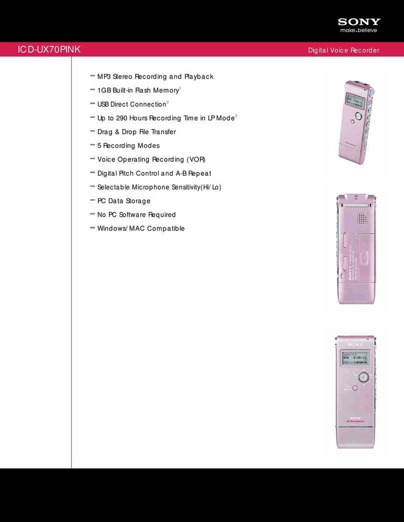
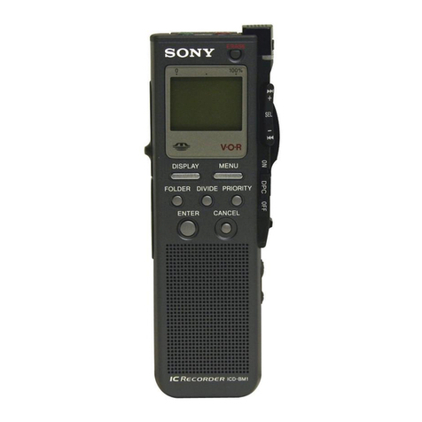
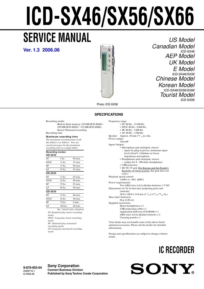
Sony M670V - M Microcassette Dictaphone User manual

M-670V/673V/675V
US Model
M-673V/675V
AEP Model
M-673V
E Model
Chinese Model
Tourist Model
M-670V
SERVICE MANUAL
MICROCASSETTE
TM
-CORDER
Sony Corporation
Personal Audio Company
Published by Sony Engineering Corporation
9-877-513-02
2004C02-1
© 2004.03
SPECIFICATIONS
Ver 1.1 2004. 03
Photo : M-670V
Model Name Using Similar Mechanism NEW
Tape Transport Mechanism Type MZ-670-99
Tape
(MICROCASSETTE)TM (normal position type)
Recording system
2-track 1-channel monaural
Speaker
Approx. 2.8 cm (11⁄8in.) dia.
Tape speed
2.4 cm/s (15⁄16 ips), 1.2 cm/s (15⁄32 ips)
Frequency range
300 - 4 000 Hz (with TAPE SPEED switch at 2.4 cm/s)
Input
Microphone input jack (minijack/monaural/PLUG IN POWER)
sensitivity 0.2 mV for 3 kΩor lower impedance microphone
Output
Earphone jack (minijack/monaural) for 8 - 300 Ωearphone
Power output (at 10% harmonic distortion)
450 mW
Power requirements
3 V DC batteries size AAA (R03) x 2/External DC 3V power
sources
Dimensions (w/h/d) (incl. projecting parts and controls)
Approx. 54.8 x 106.8 x 21.5 mm (2 1⁄4x 4 1⁄4x 7⁄8in.)
Mass (main unit only)
Approx. 92 g (3.3 oz)
Supplied accessories
AC power adaptor (1) (M-675V only), Battery charge adaptor
(1) (M-675V only), Rechargeable batteries NH-AAA, 1.2V,typ.
800 mAh, Ni-MH (2) (M-675V only), Microcassette tape MC-
30 (1) (for the United States and Europe only),Alkaline batteries
LR03 (SG) (2) (M-673V, M-670V for the United States only),
Microphone (1) (M-673V only),Carrying pouch (1) (M-
670V:JEW/M-673V only), Battery carrying case (1) (M-675V
only)
Design and specifications are subject to change without notice.
•Abbreviation
JEW: Tourist model

2
M-670V/673V/675V
TABLE OF CONTENTS
Specifications ............................................................................ 1
1. GENERAL ................................................................... 3
2. DISASSEMBLY
2-1. Cassette Lid Assy ............................................................ 4
2-2. Cabinet (Rear) ................................................................. 4
2-3. Main Board ...................................................................... 5
2-4. Mechanism Deck (MZ-670-99), LED Board ..................5
2-5. Ceramic Head (REC/PB/Erase) (HRPE901)................... 6
2-6. Motor (M901) .................................................................. 6
3. ADJUSTMENTS........................................................ 7
4. DIAGRAMS
4-1. Block Diagrams ............................................................... 9
4-2. Printed Wiring Boards– Main Section (SideA)– ............ 10
Printed Wiring Boards– Main Section (Side B)– ............ 11
4-3. Schematic Diagram ......................................................... 12
4-4. IC Block Diagrams .......................................................... 13
5. EXPLODEDVIEWS
5-1. Cabinet (Rear) Section .................................................... 14
5-2. Cabinet (Front) Section ................................................... 15
5-3. Mechanism Deck Section (MZ-670-99).......................... 16
6. ELECTRICAL PARTS LIST .................................. 17
Flexible Circuit Board Repairing
•Keep the temperature of the soldering iron around 270°C
during repairing.
•Do not touch the soldering iron on the same conductor of the
circuit board (within 3 times).
•Be careful not to apply force on the conductor when soldering
or unsoldering.
Notes on chip component replacement
•Never reuse a disconnected chip component.
•Notice that the minus side of a tantalum capacitor may be
damaged by heat.

3
M-670V/673V/675V
SECTION 1
GENERAL This section is extracted from
instruction manual.
To monitor the sound
Connect an earphone (not supplied) firmly to the EAR jack. The
monitor volume cannot be adjusted by VOL.
To prevent a cassette from being accidentally recorded
over
Break off and remove the cassette tabs. To reuse the cassette for
recording, cover the tab hole with adhesive tape.
Recording from Various Sound Sources
Notes
•When you are going to record something that you may not have an
opportunity to record again, test the unit first before you actually start
recording.
•When recording with an external microphone, the VOR system may not
work properly because of the difference in sensitivity.
Recording with an External Microphone
Connect a microphone firmly to the MIC jack.
M-673V : use the supplied microphone.
Other models : use a microphone of low impedance (less than 3
k ). When using a plug-in-power system microphone, the
power to the microphone is supplied from this unit.
Recording from another equipment
Connect another equipment firmly to the MIC jack using the
connecting cord (not supplied).
Set this unit to the recording mode and another equipment to
the playback mode.
Playing a Tape
1Insert a cassette with the side to start playing facing the lid.
2Select the tape speed to the same speed as that used for
recording.
3Press n.
4Turn VOL to adjust the volume. There is a tactile dot beside
VOL on to show the direction to turn up the volume.
At the end of the tape, playback stops and the unit turns off
automatically (Automatic shut-off mechanism). After the tape
has been wound or rewound, be sure to press Tx.
If you plug in headphones (not supplied) to the EAR jack, you
will get monaural output from both left and right channels.
To Press or slide
Stop playback/stop fast Tx
forward or rewind
Pause playback Slide >PAUSE in the direction of the
arrow. REC/BATT lamp goes off.
To release pause
playback
, release
>
PAUSE*.
Fast forward** (FF) Slide FF/CUE m•M REW/REVIEW
toward FF/CUE mduring stop.
Rewind** (REW) Slide FF/CUE m•M REW/REVIEW
toward M REW/REVIEW during stop.
Search forward during Keep FF/CUE m•M REW/REVIEW
playback (CUE) pushed toward FF/CUE m during playback
and release it at the point you want.
Search backward during Keep FF/CUE m•M REW/REVIEW
playback (REVIEW) pushed toward M REW/REVIEW during
playback and release it at the point you want.
Start recording during z
playback
*>PAUSE will also be automatically released whenTx is pressed
(stop-pause-release function).
**If you leave the unit after the tape has been wound or rewound, the
batteries will be consumed rapidly. Be sure to press Tx.
Note
If the tape is completely rewound while searching backward during
playback (REVIEW), the FF/CUE m•M REW/REVIEW switch may
not return to the center position when you release the switch. In this case,
push back the switch to the center to start playback.
To increase the playback speed
Slide the FAST PB .switch in the direction of the arrow. The
playback speed will be increased.
To return to the original speed, slide the FAST PB .switch to
the original position.
Recording
You can record right away with the built-in microphone.
Make sure that nothing is connected to the MIC jack.
1Press the reset button of the tape counter.
2Press Tx and insert a standard microcassette with the side
to start recording facing the lid.
3Select the desired tape speed.
2.4 cmfor optimum sound (recommended for normal use):
A 30-minute recording can be made using both sides of the
MC-30 microcassette (supplied for the United States and
Europe only). There is a tactile dot on this side.
1.2 cmfor longer recording time: A 60-minute recording can
be made using both sides of the MC-30 microcassette
(supplied for the United States and Europe only).
4Set VOR to OFF.
If you set VOR to ON, the unit automatically starts
recording the sound and pauses when there is no sound
(you can save tapes and batteries).
When the sound is not loud enough, set it to OFF, or the unit
may not start recording.
5Press z. nis pressed simultaneously and recording starts.
While the tape runs, the REC/BATT lamp lights and flashes
depending on the strength of the sound.
Recording level is fixed.
At the end of the tape, recording stops and the unit turns off
automatically (Automatic shut-off mechanism).
To Press or slide
Stop recording Tx
Pause recording
Slide >PAUSE in the direction of the arrow.
To release pause recording, release
>
PAUSE*.
Start recording during zduring playback (the unit enters the
playback recording mode)
Review the portion just Push up FF/CUE m•MREW/REVIEW
recorded toward MREW/REVIEW during the
recording. Release the button at the point to
start playback.
Take out a cassette Tx
*>PAUSE will also be automatically released whenTx is pressed
(stop-pause-release function).
Note
Select the 2.4 cm tape speed for recording, if you play back the recorded
tape with another unit. Otherwise, the sound quality may be changed.
Notes on VOR (Voice Operated Recording)
•The VOR system is affected by the environmental recording conditions.
When you use the system in a noisy place, the unit will stay in the
recording mode. If the sound is too soft, on the contrary, the unit will
not start recording. If you cannot get the results you want, set it to OFF.
•The VOR system may not record the beginning of the sound you want
to record because it starts recording only after it catches the sound. For
an important recording, set it to OFF.
VOL*
n*
>PAUSE
Tx
FAST PB .
TAPE SPEED* FF/CUEm•
M REW/REVIEW
EAR
E(Battery
alert LED)
*The button has a
tactile dot.
>PAUSE
Tx
EAR
VOR
TAPE SPEED*
Tape counter
z
Tx
Microphone
REC/BATT
FF/CUEm•
M REW/REVIEW
VOL*
Tape counter
reset button
MIC (PLUG IN
POWER)*
E(Battery alert
LED)
*The button/jack
has a tactile dot.
4
M-670V/673V/675V SECTION 2
DISASSEMBLY
Note: Follow the disassembly procedure in the numerical order given.
• This set can be disassembled in the order shown below.
2-1. CASSETTE LID ASSY
3-2. CABINET (REAR)
Cassette lid assySet Cabinet (rear) MAIN board
Mechanism deck (MZ-670-99), LED board Ceramic head (HRPE901)
Motor (M901)
5
cassette lid ass
y
1
eject
2
3
4
1
four screws (B1.7 x 14
)
2
claws
4
battery lid
lever (F/R)
knob (fast PB)
knob (FR)
knob (pause)
S301
S602
5
cabinet (front)
3
• CAUTIONS DURING ASSEMBLY
Align these switches and knobs
S301 tKnob (pause)
S602 t Knob (fast PB)
Lever (F/R) t Knob (FR)

5
M-670V/673V/675V
2-3. MAIN BOARD
2-4. MECHANISM DECK (MZ-670-99), LED BOARD
BLK
BLK
BLK
WHT
WHT
WHT
BLK
BRN
RED
RED
RED
1
Remove solder (sixteen places)
2
two screws
MAIN board
S501
S601
knob (tape speed) (tape speed)
knob (tape speed) (VOR)
3
• CAUTIONS DURING ASSEMBLY
Align these switches and knobs
S501 tKnob (tape speed) (VOR)
S601 t Knob (tape speed) (tape speed)
1
4
2
mechanism deck
(MZ-670-99)
3
two screws
6
LED board
5
window (BATT LED)

6
M-670V/673V/675V
2-5. CERAMIC HEAD (REC/PB/ERASE) (HRPE901)
2-6. MOTOR (M901)
1
claw
3
M1.4, special head
4
M1.4, special head
2
arm (pinch roller) ass
y
5
ceramic head
(HRPE901)
belt (flywheel)
belt (counter, tape)
How to apply the belts
belt (flywheel)
M901
flywheel assy
1
3
motor (M901)
mechanism deck
2
two screws

7
M-670V/673V/675V
3-1. MECHANICAL ADJUSTMENTS
PRECAUTION
1. Before adjusting, clean the following parts with a piece of
cotton moistened with alcohol.
record/playback/erase head pinch roller
rubber belt capstan
2. Demagnetize the record/playback/erase head using a head
demagnetizer.
3. Do not use a magnetized screwdriver for adjustments.
4. Afteradjusting, apply screw-lockingcompound to theadjusted
parts.
5. Unless specified otherwise, use a specified voltage (3V DC)
to perform the adjustments.
Torque Measurement
Tape Speed switch : 2.4cm/s
Mode Torque Meter Meter Reading
Forward CQ-103M 0.5 –0.98mN • m
(5 – 10 g • cm)
(0.07 to 0.1 38 oz• inch)
Fast Forward CQ-201M 0.5 –0.98mN • m
(5 – 10 g • cm)
(0.07 to 0.138 oz• inch)
TapeTension Measurement
Tape Speed switch : 2.4cm/s
Mode Torque Meter Meter Reading
FWD CQ-403M more than 25 g
(more than 0.9 oz)
3-2. ELECTRICAL ADJUSTMENTS
Standard Output Level
Output terminal EAR
Load impedance 8Ω
Output level 78mV (– 20dB)
TestTape
Type Signal Used for Tape speed
(cm/s)
S-2-A030A 3kHz, –20dB Azimuth Adjustment 2.4
WS-24 3kHz, –10dB Tape SpeedAdjustment 2.4
WS-12 1.2
PRECAUTION
Record/Playback/Erase Head Azimuth Adjustment
Switch position
VOLUME : Mechanical center
TAPE SPEED switch : 2.4cm/s
VOR switch : OFF
Procedure :
– FWD/REV playback –
set
test tape
S-2-A030A
(3kHz, –20dB) level mete
r
J102
earphone jack
8
Ω
• Rotate the screw to adjust level meter reading to the maximum.
Note : Adjust to the maximum peak though there may be two or
three peaks
Adjustment Location :
SECTION 3
ADJUSTMENTS
0db=0.775V
head azimath
adjustment scre
w

8
M-670V/673V/675V
Tape Speed Adjustment
Switch position
VOLUME : Mechanical center
VOR switch : OFF
Procedure :
After adjusting the 2.4cm/s speed, adjust the 1.2cm/s speed.
– Playback –
set
Test tape
WS-24, WS-12
(3kHz, –10dB) frequency counter
J102
earphone jack
8
Ω
Adjustment Value :
TestTape Adjustment Speed Frequency counter
Part
WS-24 RV602 2.4cm/s 2,880 – 3,120Hz
WS-12 RV601 1.2cm/s 2,850 – 3,150Hz
Frequency difference between the beginning and the end of the
tape should be within 0.5%.
2.4cm/s (15Hz)
1.2cm/s (15Hz)
Adjustment Location :
RV601
1.2cm/s
speed adjustable resistors
RV602
2.4cm/s
[MAIN BOARD]
(SIDE B)

M-670V/673V/675V
99
4-1. BLOCK DIAGRAMS
•Signal path.
E: PB
a: REC
SECTION 4
DIAGRAMS
10 11
14
17
19
16
6
9
2
5
6
14
15
4
13
2
20
DRIVE
FEEDBACK
POWER ON
DETECT
Q307
LED
DRIVER
Q703, 706
F F OSC
Q704
OSC
LOGIC
CIRCUITY
S101 (2/4)
REC PB
S101 (4/4)
REC PB
RIPPLE
FILTER
7
1
REC
ALC
REC
VOR
VOR
DETECT
Q305
J101
MIC
(PLUG IN POWER)
MIC1
MIC
S101
(1/4, 3/4)
REC PB
Q301
M901
CAPSTAN/
REEL
MOTOR
D701
REC/BATT
D302
HRPE901
REC/PB
HEAD
ERASE
HEAD
+B
U OUT
V OUT
W OUT
VCC
U
V
W
Q306
Q601
RV601
TAPE SPEED
(1.2cm)
RV601
S602
FAST PB
ON
OFF
VCC
+VCC
VREF
IN+
S/S
S601 (2/2)
TAPE SPEED
1.2cm 2.4cm
RV602
TAPE SPEED
(2.4cm)
S601 (1/2)
TAPE SPEED
2.4cm
1.2cm
PRE AMP
IC101 (1/2)
BTL POWER AMP
IC101 (2/2)
NC RFLT IN
PRE OUT
RFLT
OUT
+VCC
PRE2 IN
PRE2 NF
22 REG
REG OUT
SP IN
ALC IN
Q304
MUTE
MOTOR DRIVER
IC601
S102
(POWER)
+VCC
S501
VOR
OFF
ON
J102
EAR
SP1
(SPEAKER)
S301
PAUSE
ON
OFF
RV101
VOL
D702
J901
DC IN 3V
DRY BATTERY
SIZE "AAA"
(IEC DESIGNATION R03)
2PCS, 3V
23
+1.7V REG.
IC401
VOUT
VDD
21
LEVEL DETECT
IC701
VOUT VDD
+VCC
+VCC
Q303
Q702
Q302
3
21
PRE1 OUT
PRE1 NF
PRE1 IN
5
23
LED
DRIVER
Q701
+B
SWITCH
Q705
DELAY

M-670V/673V/675V
1010
4-2. PRINTED WIRING BOARD – MAIN BOARD (SIDE A) –
R706
R707
R702
E B C
Q701
C B E
Q702
R311
R323
R312
S601
S601
S501
R103
R104
R105
R607
C314
C311
C303
R324
C301
D302
R703
D701
REC
BATT
R708
C701
C306
C108
C317
C304
C307 C302
C121
C305
C502
C504
C501
C105
C110
C106
C703
R608
R612
TH601
R616
S102
(POWER)
S602
C312
R614
C706
Q706
Q601
Q703
IC601
11
20
10
1
C605
C309
ON OFF
t
VOR
2.4cm 1.2cm
t
TAPE SPEED
ON OFF
t
FAST PB
.
(SIDE A)
BOARDMAIN
11
(11)
1-860-838-
E C B
E C B
E C B
E C B
23 4 5 6 7 8
A
1
B
C
D
E
Ref. No. Location
D302 D-4
D701 A-1
IC601 C-6
Q601 B-7
Q701 B-2
Q702 A-2
Q703 C-7
Q706 C-7
• Semiconductor
Location
Note:
•X: parts extracted from the component side.
•r: Through hole.
•: Pattern from the side which enables seeing.
(The other layers' patterns are not indicated.)
Caution:
Pattern face side: Partson thepattern faceside seenfrom
(Conductor B) the pattern face are indicated.
Parts face side: Parts on the parts face side seen from
(Component A) the parts face are indicated.

M-670V/673V/675V
1111
PRINTED WIRING BOARD – MAIN BOARD (SIDE B) –
B C E
E C B
E C B
E C B
E C B
E C B
E C B
B C E
R606
R605
C608C606
R603
R124
C505
R502
R310
R301
C111
R717
R318
D301
R313
R319
R314
R125 C122
C124
R320
R315
S301
R714
C704
R709
R716
R611
C601
C315
C609
C604
C607
C119
R114
C308
R109
R110
C310
R119
R118
R201
R307
C107
R308
R304
R305
R302
C101
C103
R306
R317
C102
R321
R112
C112
R322
C125
R127
R126 C320
C117
C104
C120
R106
R107
12 1
13 24
R111
C109
C114
C118
R113
R120
C123
Q304
Q705
C C
B E B
Q704
C318
C705
C602 R601
R621
R602
R610
R604
R713
R712
SL301
TP28
TP23
TP20
TP17
TP32
Q305 Q307
Q303
TP21 TP18
TP15
TP34
TP17
IC701
IC401
TP17
TP14
W704
W703
W301
U
V
W
VCC
W302
W102 W101
W104
W103
TP26
RV602 RV601
TP33
TP25
IC101
TP22
TP16
TP13
TP12
TP7
Q301
Q302
Q306
TP10
TP6 TP9
TP19
TP4
TP24
TP31
TP40
TP30
TP29
1
-1 -2
-3 -4
2
3
4
12
3
4
RV101
N
VOL
MIC1
MIC
J101
MIC
(PLUG IN POWER)
J102
EAR
1
2
4
3
1
2
43
HRPE901
RECORD/
PLAYBACK/
ERASE
HEAD
SP1
SPEAKER
S101
REC
PB
t
PAUSE
.
ON OFF
t
W904
W701
W702
D702
W902
DRY BATTERY
SIZE "AAA"
(IEC DESIGNATION R03)
2PCS, 3V
11
(11)
1-860-839-
11
(11)
1-860-838-
(SIDE B)
BOARDMAIN
BOARDLED
W
V
U
VCC
M901
CAPSTAN/REEL
MOTOR
DC IN 3V
J901
23 4 5 6 7 89 10
A
1
B
C
D
E
F
Ref. No. Location
D301 B-5
D702 B-1
IC101 D-6
IC401 D-7
IC701 B-4
Q301 D-7
Q302 D-7
Q303 B-6
Q304 C-6
Q305 B-5
Q306 D-7
Q307 B-6
Q704 B-4
Q705 B-4
• Semiconductor
Location
Note:
•X: parts extracted from the component side.
•r: Through hole.
•: Pattern from the side which enables seeing.
(The other layers' patterns are not indicated.)
Caution:
Pattern face side: Partson thepattern faceside seenfrom
(Conductor B) the pattern face are indicated.
Parts face side: Parts on the parts face side seen from
(Component A) the parts face are indicated.

M-670V/673V/675V
1212
4-3. SCHEMATIC DIAGRAM
IC601
IC101
D701
D301
S601(2/2)
S601(1/2)
D302
R314
C101
C103
C104
C105
C106
C110
C123
C304 C317
C107
C302
C501
C502
C504 C505
C309
C312
C121
C303
C305
C109
C306
C112
C124
C307
C114
C122
C318
C601
C604
C607
C609
C602
C606
C608
C701
C703
C704
C706
C605
R302
R304
R305
R321
R322
C320
R109 R124
R103
R104
R105
R306
R307 R308
R323
R324
C301
R709
R717
R702
R703
R706
R707
R708
R712 R713 R714 R716
R602
R603 R605
R607
R608 R612
R614
S301
R610 R611 R616
J102
MIC1
R312
R118
R119
R201
R112
R113
R114
C119
R120
R125
R311
R310
R319
R315
R318
R313
R604
R621 R601
S602
Q703
Q704
Q706
Q701
Q601
Q301
Q705
Q307
IC701
R301
RV601
RV602
Q303
R320
RV101
C120
C117
C314
C315
THP601
C310
R317
S102
S101(2/4)
S101(4/4)
S101(1/4)
S101(3/4)
SP1
Q305
Q304
Q702
C308
C108
R106
R107
C125
R126 R127 C111 R110
R111
S501
C705
C311
Q302
J901
J101
R606
HRPE901
R502
D702
IC401
C102
Q306
LB1979VS-TLM-E
BH3682FV
SML-310LTT86
1SS355TE-17
1SS355TE-17
1k
0.1
0.01
0.01
0.01
0.022
2200
1
22
6.3
22
6.3
1
10V
10
10V
4.7
4V
1
0.01 0.047
10
10V
10
10V
10
10V
220
4V
2.2
0.01
2.2
0.47
0.01
4.7
4V
0.22
4700p
1
0.47
2.2
0.047
0.22
0.047
0.047
0.047
0.47
1
1
22
6.3V
10
10V
1k
10k
22k
470
470
1
10k 2.2k
10k
22k
4.7k
47k
47k 22k
4.7k
10k
22
6.3V
1k
4.7k
1k
220
1k
1M
2.2k
470k 22k 22k 470k
1M
1M 1M
4.7k
4.7k 4.7k
1k
22k 47k 470
22
220
1k
22
2.2k
2.2k
220k
C118
100p
0.01
1k
1k
1M
470
220k
4.7k
22k
2.2k
100k
2.2k 1k
UN9114J-(TX).SO
LED DRIVER
XP1501
F.F OSC
UN9214J-(TX).SO
LED DRIVER
XP4601
LED DRIVER
SSM3K03FE(TPL3)
SWITCH
UN9215J-(TX).SO
SWITCH
UN9115J-(TX).SO
+B SWITCH
UN9214J-(TX).SO
POWER ON
DETECT
PST3720UL
LEVEL
DETECT
22
4.7k
4.7k
2SA1774R
SWITCH
2.2k
5k
0.022
1000p
220
4V
1000p
1
100k
(POWER)
2SA1774R
VOR
DETECT
2SC4213-AB-TE85L
MUTE
UN9215J-(TX).SO
INVERTER
2.2
10
10V
220
1k 0.01
470 1k 0.1 47k
22k
1
220
4V
DTC144EE
INVERTER
22k
4.7k
SML-311YTT86
MM3031HULE
+1.7V REG.
0.022
UN9114J-(TX).SO
SWITCH
WB
VCC
NC
UOUT
P-GND
VB
UB
GND
WOUT
V OUT
FC GND
FC
R1
OUT
IN+
VREF
COM
OSC
VSP
S/S
PRE1 NF
REG OUT
PRE1 OUT
PRE2 IN
VOR TAU
VOR C
VOR IN
VOR OUT
SP BIAS
SP2 OUT
PWRVCC
PRE1 IN
PRE GND
PRE2 NF
VOR CTRL
PRE2 OUT
ALC TAU
ALC DETIN
SP IN
SP1 OUT
SP GND
GND
VDD
CE
VOUT
V OUT
VDD
VSS
NC
DC IN 3V
MOTOR
M901
CAPSTAN/REEL
PB REC
PB REC
PB REC
PB REC
ON
OFF
VOR
ON
OFF
ON OFF
FAST PB
MOTOR
DRIVER
PRE AMP,
BTL
POWER AMP
MIC
(PLUG IN POWER)
MIC
PAUSE
TAPE SPEED
(2.4cm)
TAPE SPEED
(1.2cm)
VOL
EAR
SPEAKER
TAPE SPEED
TAPE SPEED
HEAD
ERASE
PLAYBACK/
RECORD/
PRE VCC
RFLTIN
RFLTOUT
DRY BATTERY
SIZE"AAA"
(IEC DESIGNATION R03)
2PCS,3V
REC BATT

13
M-670V/673V/675V
4-4. IC Block Diagrams
IC101 BH3682FV
IC601 LB1979VS-TLM-E
1211109
8
765431
131415
16171819
20
21
22
23
24
PREVCC
PREINF
RFLTOUT
RFLTIN
REG
PRE1OUT
MICALCIN
VORTAU
VORC
VORIN
VOROUT
REC/BIAS
REC/SP2OUT
PWRVCC
PREIIN
GND
ALCNF
VORCTRL
MICALCOUT
ALCTAU
ALCDETIN
REC/SPIN
REC/SP1OUT
SPGND
BH3682FV
TapeRecorder
PRE/PWR
MIC/REC
PREVCC
PWRCTRL
PRE1
31dB
MICALC/PRE2
delta: 40dB
BIAS
26dB
PWRVCC
INV
VORCTRL
PRE PWR
POM
37dB
REC/POWER
22dBSE 0dBSE
REC
ALC
REG RBC
VOR
RIPL
2
+
-
+-
ZZ
INV
FC GND
VCC
VCC
FC
WB
VCC
NC
UOUT
VOUT
WOUT
P-GND
VB
UB
GND
TO
CONTROL
BLOCKS
TO
EACH
BLOCKS
RI
OUT
VSP
IN+
VREF
S/S
COM
OSC
75
4
31 2 6 8 9 10
1112131415161820 19
STARTING
DETECT
POWER
SUPPLY
BIAS
OSCILLATING
CIRCUIT
SPEED CONTROL
REFERENCE VOLTAGE
REFERENCE
VOLTAGE
CURRENT
DETECT
SPEED
DETECT
WAVEFORM DETECT
COMMUTATION STARTING LOGIC
SOFT SWITCH
PRE DRIVER
+
–
17
Note on Schematic Diagram:
•All capacitors are in µF unless otherwise noted. pF: µµF 50 WV or less are not indicated
except for electrolytics and tantalums.
•All resistors are in Ωand 1/4W or less unless otherwise specified.
•A: B+ Line.
•H: adjustment for repair.
•Power voltage is dc 3 V and fed with regulated dc power supply from battery terminal.
•Voltages and waveforms are dc with respect to ground in service mode.
no mark : PLAY
():REC
•Voltages are dc with a VOM (Input impedance 10 MΩ).
Voltage variations may be noted due to normal production tolerances.
•Signal path.
E: PB
a: REC
•WAVEFORMS
IC601 qa OSC
VOL/DIV : 20m V AC
TIME/DIV : 1m sec
1
40m Vp-
p
1.6m sec

14
M-670V/673V/675V
Ref. No. Part No. Description Remarks Ref. No. Part No. Description Remarks
SECTION 5
EXPLODED VIEWS
5-1. CABINET (REAR) SECTION
NOTE:
•-XX, -X mean standardized parts, so they may
have some differences from the original one.
•Items marked “*” are not stocked since they
are seldom required for routine service. Some
delayshould be anticipated when ordering these
items.
•Themechanical parts with noreferencenumber
in the exploded views are not supplied.
•Hardware (# mark) list and accessories are
given in the last of this parts list.
•Abbreviation
CH : Chinese model
JEW : Tourist model
1E : No indication of country of origin
1
2
2
3
4
5
67
8
cabinet (front) section
13-258-296-11 CABINET (REAR)(670V:CH,E,JEW/673V:US/675V)
13-258-296-21 CABINET (REAR) (670V:1E,EE/673V:AEP)
23-318-203-99 SCREW (B1.7X14), TAPPING
33-258-297-01 KNOB (PAUSE)
43-258-300-01 KNOB (FR)
53-258-299-01 KNOB (FAST PB)
63-258-304-01 LID, BATTERY
7 3-258-286-01 TERMINAL (+.-), BATTERY
83-258-301-01 PAPER, SHIELD
Ver 1.1

15
M-670V/673V/675V
5-2. CABINET (FRONT) SECTION
Ref. No. Part No. Description Remarks Ref. No. Part No. Description Remarks
MIC1
mechanism deck section
(MZ-670-99)
SP1
not supplied
51
51
53
54
55 57
58
59
56
60
70
61
52
62 63
64
65
66
67 68
69
51 3-704-197-31 LOCK, SERRAT IB
52 3-831-441-99 SPACER, KNOB
*53 A-4541-601-A MAIN BOARD, COMPLETE
54 3-375-114-71 SCREW
*55 1-860-839-11 LED BOARD
56 3-258-294-01 TERMINAL (+), BATTERY
57 3-258-293-01 BUTTON (REC)
58 3-258-292-01 BUTTON (PLAY)
59 3-258-291-01 BUTTON (STOP)
60 3-258-319-01 WINDOW (BATT LED)
61 3-318-203-72 SCREW (B1.7X5), TAPPING
62 3-258-287-01 HOLDER, BATTERY
63 3-328-319-01 STRAP, HAND
64 3-258-285-11 CABINET (FRONT)
65 X-3384-510-1 LID ASSY, CASSETTE
66 3-258-298-01 KNOB (TAPE SPEED)
67 3-258-288-01 WINDOW (REC LED)
68 3-258-289-01 CUSHION, MICROPHONE
69 3-258-290-01 CASE, MICROPHONE
70 3-262-078-01 PLATE, ORNAMENTAL
MIC1 1-476-484-31 MICROPHONE UNIT, ELECTRET CAP
*SP1 1-825-656-11 LOUD SPEAKER

16
M-670V/673V/675V
5-3. MECHANISM DECK SECTION (MZ-670-99)
M901
HRPE901
101
102
102
103
104
105
106
107
108
109
110
111
112
113
114
115
116
117
118
119
120 121
122
142
143
140
123 124
125
126
127 128
129
130
131
132
138 139 141
137
133
134
135
107
102
Ref. No. Part No. Description Remarks Ref. No. Part No. Description Remarks
101 3-028-965-01 SPRING (PINCH ARM), TORSION
102 3-365-611-11 SCREW (M1.4X1.4), SPECIAL HEAD
103 3-232-536-22 SCREW (M1.4) (EG)
104 3-028-960-02 SPRING (AZIMUTH), COMPRESSION
105 3-028-909-13 GUIDE (N), TAPE
*106 3-029-640-03 BRACKET (OW), HEAD
107 3-331-007-21 WASHER
108 3-350-989-01 WASHER
109 3-028-961-02 SPRING (BUTTON), COMPRESSION
110 3-028-924-07 LEVER (PLAY)
111 X-3384-067-1 ARM (PINCH ROLLER) ASSY (C)
112 3-046-281-11 LEVER (POWER SW) (B)
113 3-028-940-05 LEVER (SRS)
114 3-028-938-06 LEVER (SLIDE)
115 3-578-224-00 WASHER
116 X-3376-227-4 LEVER (F/R) ASSY
117 X-3376-228-9 LEVER (TU) ASSY
118 3-029-634-15 BEARING
119 X-3376-231-2 FLYWHEEL ASSY
120 3-377-420-11 BELT
121 X-3376-224-7 LEVER (REC) ASSY
122 3-029-641-01 SPRING, TORSION
123 3-028-957-01 SPRING (CAM GEAR),TENSION
124 3-028-966-14 GEAR (S-OFF-OW), CAM
125 X-3376-230-5 LIMITTER ASSY
126 3-028-955-02 SPRING (LOCK), TENSION
127 X-3377-535-5 LEVER (LOCK) ASSY
128 4-992-239-01 WASHER (A)
*129 3-028-967-05 LEVER (PAUSE RELEASE)
130 3-028-954-03 SPRING (SW LEVER), TENSION
131 3-321-813-71 WASHER, COTTER POLYETHYLENE
132 3-028-928-06 LEVER (EJECT)
133 3-028-964-02 SPRING (SLIDE), TORSION
134 4-926-562-01 WASHER, STOPPER
135 3-028-927-05 LEVER (STOP)
137 1-548-579-41 COUNTER, TAPE (SMALL TYPE)
138 X-3384-068-1 CHASSIS (COMP) ASSY (C)
139 3-343-948-01 BELT
140 4-963-883-61 SCREW (M1.4), PRECISION PAN
141 3-365-053-01 SHEET (BA), ADHESIVE
142 3-378-078-11 SPACER (END DETECTION)
143 3-037-211-02 REINFORCEMENT (MJ)
HRPE901 1-500-593-13 HEAD, CERAMIC (REC/PB/ERASE)
M901 1-787-144-11 MOTOR, DC (CAPSTAN/REEL) (including PULLY)

17
M-670V/673V/675V
SECTION 6
ELECTRICAL PARTS LIST
Ref. No. Part No. Description Remarks Ref. No. Part No. Description Remarks
NOTE:
•Due to standardization, replacements in the
parts list may be different from the parts
specifiedin the diagrams orthecomponents
used on the set.
•-XX, -X mean standardized parts, so they
may have some difference from the original
one.
•Itemsmarked “*” are notstocked since they
are seldom required for routine service.
Some delay should be anticipated when
ordering these items.
•CAPACITORS:
uF: µF
•RESISTORS
All resistors are in ohms.
METAL: metal-film resistor
METAL OXIDE: Metal Oxide-film resistor
F: nonflammable
•COILS
uH: µH
•SEMICONDUCTORS
In each case, u: µ, for example:
uA...: µA... , uPA... , µPA... ,
uPB... , µPB... , uPC... , µPC... ,
uPD..., µPD...
•Abbreviation
CH : Chinese model
JEW : Tourist model
1E : No indication of country of origin
*1-860-839-11 LED BOARD
*********
3-258-294-01 TERMINAL (+), BATTERY
< DIODE >
D702 8-719-060-92 DIODE SML-311YTT86 (E)
************************************************************
*A-4541-601-A MAIN BOARD, COMPLETE
*******************
3-036-882-02 SPACER (JACK)
< CAPACITOR >
C101 1-125-777-11 CERAMIC CHIP 0.1uF 10% 10V
C102 1-107-819-11 CERAMIC CHIP 0.022uF 10% 16V
C103 1-164-943-11 CERAMIC CHIP 0.01uF 10% 16V
C104 1-164-943-11 CERAMIC CHIP 0.01uF 10% 16V
C105 1-164-943-11 CERAMIC CHIP 0.01uF 10% 16V
C106 1-107-819-11 CERAMIC CHIP 0.022uF 10% 16V
C107 1-135-208-11 TANTAL. CHIP 1uF 20% 10V
C108 1-104-851-11 TANTAL. CHIP 10uF 20% 10V
C109 1-164-943-11 CERAMIC CHIP 0.01uF 10% 16V
C110 1-164-939-11 CERAMIC CHIP 0.0022uF 10% 50V
C111 1-125-777-11 CERAMIC CHIP 0.1uF 10% 10V
C112 1-117-863-11 CERAMIC CHIP 0.47uF 10% 6.3V
C114 1-115-467-11 CERAMIC CHIP 0.22uF 10% 10V
C117 1-164-937-11 CERAMIC CHIP 0.001uF 10% 50V
C118 1-164-874-11 CERAMIC CHIP 100pF 5% 50V
C119 1-164-943-11 CERAMIC CHIP 0.01uF 10% 16V
C120 1-107-819-11 CERAMIC CHIP 0.022uF 10% 16V
C121 1-104-851-11 TANTAL. CHIP 10uF 20% 10V
C122 1-164-941-11 CERAMIC CHIP 0.0047uF 10% 16V
C123 1-115-156-11 CERAMIC CHIP 1uF 10V
C124 1-164-943-11 CERAMIC CHIP 0.01uF 10% 16V
C125 1-162-970-11 CERAMIC CHIP 0.01uF 10% 25V
C301 1-119-750-11 TANTAL. CHIP 22uF 20% 6.3V
C302 1-104-851-11 TANTAL. CHIP 10uF 20% 10V
C303 1-113-690-11 ELECT CHIP 220uF 20% 4V
C304 1-119-750-11 TANTAL. CHIP 22uF 20% 6.3V
C305 1-135-834-91 CERAMIC CHIP 2.2uF 6.3V
C306 1-135-834-91 CERAMIC CHIP 2.2uF 6.3V
C307 1-135-151-21 TANTALUM CHIP 4.7uF 20% 4V
C308 1-135-834-91 CERAMIC CHIP 2.2uF 6.3V
C309 1-104-851-11 TANTAL. CHIP 10uF 20% 10V
C310 1-115-156-11 CERAMIC CHIP 1uF 10V
C311 1-126-246-11 ELECT CHIP 220uF 20% 4V
C312 1-104-851-11 TANTAL. CHIP 10uF 20% 10V
C314 1-126-246-11 ELECT CHIP 220uF 20% 4V
C315 1-164-937-11 CERAMIC CHIP 0.001uF 10% 50V
C317 1-119-750-11 TANTAL. CHIP 22uF 20% 6.3V
C318 1-115-156-11 CERAMIC CHIP 1uF 10V
C320 1-115-156-11 CERAMIC CHIP 1uF 10V
C501 1-135-151-21 TANTALUM CHIP 4.7uF 20% 4V
C502 1-115-156-11 CERAMIC CHIP 1uF 10V
C504 1-164-943-11 CERAMIC CHIP 0.01uF 10% 16V
C505 1-119-923-11 CERAMIC CHIP 0.047uF 10% 10V
C601 1-117-863-11 CERAMIC CHIP 0.47uF 10% 6.3V
C602 1-119-923-11 CERAMIC CHIP 0.047uF 10% 10V
C604 1-125-838-11 CERAMIC CHIP 2.2uF 10% 6.3V
C605 1-104-851-11 TANTAL. CHIP 10uF 20% 10V
C606 1-119-923-11 CERAMIC CHIP 0.047uF 10% 10V
C607 1-119-923-11 CERAMIC CHIP 0.047uF 10% 10V
C608 1-119-923-11 CERAMIC CHIP 0.047uF 10% 10V
C609 1-115-467-11 CERAMIC CHIP 0.22uF 10% 10V
C701 1-113-619-11 CERAMIC CHIP 0.47uF 10V
C703 1-115-156-11 CERAMIC CHIP 1uF 10V
C704 1-115-156-11 CERAMIC CHIP 1uF 10V
C705 1-115-156-11 CERAMIC CHIP 1uF 10V
C706 1-119-750-11 TANTAL. CHIP 22uF 20% 6.3V
< DIODE >
D301 8-719-988-61 DIODE 1SS355TE-17
D302 8-719-988-61 DIODE 1SS355TE-17
D701 8-719-064-07 DIODE SML-310LTT86 (REC BATT)
< IC >
IC101 6-704-794-01 IC BH3682FV
IC401 6-705-813-01 IC MM3031HULE
IC601 8-759-638-51 IC LB1979VS-TLM-E
IC701 6-704-872-01 IC PST3720UL
< JACK >
J101 1-785-790-11 JACK (MIC (PLUG IN POWER))
J102 1-785-791-11 JACK (EAR)
J901 1-794-615-11 JACK,DC(POLARITY UNIFIED TYPE) (DC IN 3V)
< TRANSISTOR >
Q301 8-729-037-76 TRANSISTOR UN9215J-(TX).SO
When indicating parts by reference
number, please include the board.
The components identified by mark 0
or dotted line with mark 0are critical
for safety.
Replace only with part number specified.
LED MAIN
Ver 1.1

18
M-670V/673V/675V
Ref. No. Part No. Description Remarks Ref. No. Part No. Description Remarks
MAIN
Q302 8-729-928-81 TRANSISTOR DTC144EE
Q303 8-729-928-19 TRANSISTOR 2SA1774R
Q304 8-729-013-37 TRANSISTOR 2SC4213-AB-TE85L
Q305 8-729-928-19 TRANSISTOR 2SA1774R
Q306 8-729-037-62 TRANSISTOR UN9114J-(TX).SO
Q307 8-729-037-75 TRANSISTOR UN9214J-(TX).SO
Q601 8-729-047-68 TRANSISTOR SSM3K03FE(TPL3)
Q701 8-729-427-74 TRANSISTOR XP4601
Q702 8-729-037-76 TRANSISTOR UN9215J-(TX).SO
Q703 8-729-037-62 TRANSISTOR UN9114J-(TX).SO
Q704 8-729-429-44 TRANSISTOR XP1501
Q705 8-729-037-63 TRANSISTOR UN9115J-(TX).SO
Q706 8-729-037-75 TRANSISTOR UN9214J-(TX).SO
< RESISTOR >
R103 1-218-965-11 RES-CHIP 10K 5% 1/16W
R104 1-218-969-11 RES-CHIP 22K 5% 1/16W
R105 1-218-961-11 RES-CHIP 4.7K 5% 1/16W
R106 1-218-945-11 RES-CHIP 220 5% 1/16W
R107 1-218-953-11 RES-CHIP 1K 5% 1/16W
R109 1-218-965-11 RES-CHIP 10K 5% 1/16W
R110 1-218-973-11 RES-CHIP 47K 5% 1/16W
R111 1-218-969-11 RES-CHIP 22K 5% 1/16W
R112 1-218-957-11 RES-CHIP 2.2K 5% 1/16W
R113 1-218-957-11 RES-CHIP 2.2K 5% 1/16W
R114 1-218-981-11 RES-CHIP 220K 5% 1/16W
R118 1-218-945-11 RES-CHIP 220 5% 1/16W
R119 1-218-953-11 RES-CHIP 1K 5% 1/16W
R120 1-218-953-11 RES-CHIP 1K 5% 1/16W
R124 1-218-957-11 RES-CHIP 2.2K 5% 1/16W
R125 1-218-953-11 RES-CHIP 1K 5% 1/16W
R126 1-218-949-11 RES-CHIP 470 5% 1/16W
R127 1-218-953-11 RES-CHIP 1K 5% 1/16W
R201 1-218-933-11 RES-CHIP 22 5% 1/16W
R301 1-218-933-11 RES-CHIP 22 5% 1/16W
R302 1-218-953-11 RES-CHIP 1K 5% 1/16W
R304 1-218-965-11 RES-CHIP 10K 5% 1/16W
R305 1-218-969-11 RES-CHIP 22K 5% 1/16W
R306 1-218-973-11 RES-CHIP 47K 5% 1/16W
R307 1-218-973-11 RES-CHIP 47K 5% 1/16W
R308 1-218-969-11 RES-CHIP 22K 5% 1/16W
R310 1-218-949-11 RES-CHIP 470 5% 1/16W
R311 1-218-989-11 RES-CHIP 1M 5% 1/16W
R312 1-218-933-11 RES-CHIP 22 5% 1/16W
R313 1-218-957-11 RES-CHIP 2.2K 5% 1/16W
R314 1-218-953-11 RES-CHIP 1K 5% 1/16W
R315 1-218-961-11 RES-CHIP 4.7K 5% 1/16W
R317 1-218-977-11 RES-CHIP 100K 5% 1/16W
R318 1-218-969-11 RES-CHIP 22K 5% 1/16W
R319 1-218-981-11 RES-CHIP 220K 5% 1/16W
R320 1-218-957-11 RES-CHIP 2.2K 5% 1/16W
R321 1-218-949-11 RES-CHIP 470 5% 1/16W
R322 1-218-949-11 RES-CHIP 470 5% 1/16W
R323 1-218-961-11 RES-CHIP 4.7K 5% 1/16W
R324 1-218-965-11 RES-CHIP 10K 5% 1/16W
R502 1-218-961-11 RES-CHIP 4.7K 5% 1/16W
R601 1-218-953-11 RES-CHIP 1K 5% 1/16W
R602 1-218-989-11 RES-CHIP 1M 5% 1/16W
R603 1-218-989-11 RES-CHIP 1M 5% 1/16W
R604 1-218-977-11 RES-CHIP 100K 5% 1/16W
R605 1-218-989-11 RES-CHIP 1M 5% 1/16W
R606 1-218-969-11 RES-CHIP 22K 5% 1/16W
R607 1-218-961-11 RES-CHIP 4.7K 5% 1/16W
R608 1-218-961-11 RES-CHIP 4.7K 5% 1/16W
R610 1-218-969-11 RES-CHIP 22K 5% 1/16W
R611 1-218-973-11 RES-CHIP 47K 5% 1/16W
R612 1-218-961-11 RES-CHIP 4.7K 5% 1/16W
R614 1-218-953-11 RES-CHIP 1K 5% 1/16W
R616 1-218-985-11 RES-CHIP 470K 5% 1/16W
R621 1-218-957-11 RES-CHIP 2.2K 5% 1/16W
R702 1-218-953-11 RES-CHIP 1K 5% 1/16W
R703 1-218-945-11 RES-CHIP 220 5% 1/16W
R706 1-218-953-11 RES-CHIP 1K 5% 1/16W
R707 1-218-989-11 RES-CHIP 1M 5% 1/16W
R708 1-218-957-11 RES-CHIP 2.2K 5% 1/16W
R709 1-218-953-11 RES-CHIP 1K 5% 1/16W
R712 1-218-985-11 RES-CHIP 470K 5% 1/16W
R713 1-218-969-11 RES-CHIP 22K 5% 1/16W
R714 1-218-969-11 RES-CHIP 22K 5% 1/16W
R716 1-218-985-11 RES-CHIP 470K 5% 1/16W
R717 1-218-961-11 RES-CHIP 4.7K 5% 1/16W
< VARIABLE RESISTOR >
RV101 1-227-611-11 RES, VAR, CARBON 5K (VOLw)
RV601 1-225-668-11 RES, ADJ, CERMET 4.7K (TAPE SPEED (1.2cm))
RV602 1-225-668-11 RES, ADJ, CERMET 4.7K (TAPE SPEED (2.4cm))
< SWITCH >
S101 1-786-656-11 SIGNAL SELETOR SWITCH (REC/PB)
S102 1-762-594-41 SWITCH, PUSH (1 KEY) (POWER)
S301 1-572-922-11 SWITCH, SLIDE ( PAUSE)
S501 1-572-922-11 SWITCH, SLIDE (VOR)
S601 1-571-277-51 SWITCH, SLIDE (TAPE SPEED)
S602 1-572-922-11 SWITCH, SLIDE (FAST PB)
< THERMISTOR >
THP601 1-803-124-11 THERMISTOR, POSITIVE
******************************************************
MISCELLANEOUS
*************
137 1-548-579-41 COUNTER, TAPE (SMALL TYPE)
HRPE901 1-500-593-13 HEAD, CERAMIC (REC/PB/ERASE)
M901 1-787-144-11 MOTOR, DC (CAPSTAN/REEL) (including PULLY)
MIC1 1-476-484-31 MICROPHONE UNIT, ELECTRET CAP
*SP1 1-825-656-11 LOUD SPEAKER
************************************************************
ACCESSORIES
***********
01-477-102-11 ADAPTOR, AC (AC-E300) (675V)
01-478-440-11 BATTERY CHARGER (675V)
1-542-564-11 MICROPHONE (673V)
1-756-415-21 BATTERY, NICKEL HYDROGEN (675V)
*2-283-326-01 LABEL, CAUTION (670V:JEW)
.
The components identified by
mark 0or dotted line with mark
0are critical for safety.
Replace only with part number
specified.
Ver 1.1

19
M-670V/673V/675V
3-220-749-01 CASE, CARRYING (for set)(670V:JEW,673V)
3-259-967-01 MANUAL, INSTRUCTION (JAPANESE)(670V:JEW)
3-259-967-11 MANUAL, INSTRUCTION
(ENGLISH, SPANISH)(673V:US,675V)
3-259-967-31 MANUAL, INSTRUCTION
(ENGLISH,SPANISH,ITALIAN,PORTUGUESE)
(670V:E)
3-259-967-51 MANUAL, INSTRUCTION (ENGLISH,RUSSIAN)
(670V:EE)
3-259-967-61 MANUAL, INSTRUCTION
(CZECH,HUNGARIAN,POLISH,SLOVAKIAN)
(670V:EE)
3-259-967-71 MANUAL, INSTRUCTION
(ENGLISH,SIMPLIFIED CHINESE)(670V:CH)
3-259-967-81 MANUAL, INSTRUCTION
(ENGLISH,TRADITIONAL CHINESE)(670V:1E)
3-259-967-91 MANUAL, INSTRUCTION
(ENGLISH,TRADITIONAL CHINESE,KOREAN,
RUSSIAN)(670V:JEW)
Ref. No. Part No. Description Remarks
Ver 1.1

M-670V/673V/675V
REVISION HISTORY
Clicking the version allows you to jump to the revised page.
Also, clicking the version at the upper right on the revised page allows you to jump to the next revised
page.
Ver. Date Description of Revision
1.0 2004.02 New
1.1 2004.03 Delete of M-670V Canadian andAEP models. (ENG-04009)
Other manuals for M670V - M Microcassette Dictaphone
4
This manual suits for next models
2
Table of contents
Other Sony Voice Recorder manuals

Sony
Sony ICD-P320 Digital Voice Editor 2 User manual

Sony
Sony FS-85USB - Foot Control Unit User manual

Sony
Sony BM-575A - Portable Microcassette Dictating... User manual

Sony
Sony ICD-P17 - Ic Recorder User manual

Sony
Sony ICD-R100 Operating Instructions (primary... User manual

Sony
Sony ICD-UX523 User manual

Sony
Sony ICD-BP150VTP Marketing User manual

Sony
Sony ICD-BM1A - Memory Stick Media Digital Voice... Reference guide

Sony
Sony SRR1 Quick start guide

Sony
Sony ICDBM1 - Memory Stick Media Digital Voice... User manual