ST STDES-WBC86WTX Instructions for use

Introduction
The STDES-WBC86WTX reference design, based on STWBC86, is designed for wireless power transmitter applications. It
allows the user to start a 2.5 W wireless charging project quickly.
The integrated circuit requires only a few external components, such as ASK (Qi based communication) demodulation circuit.
The board can work with 5 to 12 V input voltage.
Using an external USB-to-I²C converter, you can monitor and control the STWBC86 using the STSW-WPSTUDIO GUI.
The STDES-WBC86WTX includes several safety mechanisms that provides overtemperature (OTP), overcurrent (OCP), and
overvoltage (OVP) protections.
The STDES-WBC86WTX is a fully assembled reference design developed for performance evaluation only, not available for
sale.
This document summarizes the following fundamental evaluation steps:
• Power-up test
• ASK demodulation test
• Efficiency test
• Thermal performance test
STDES-WBC86WTX Wireless Power Transmitter Quick Start Guide and Test
Report
TN1442
Technical note
TN1442 - Rev 2 - August 2023
For further information contact your local STMicroelectronics sales office.
www.st.com

1 Overview
To get started with the STDES-WBC86WTX, you need the following equipment:
•STDES-WBC86WTX
• Additional hardware:
– 1 x USB adapter 5 V/1.5 A or power supply
– 1 x USB cable (can be replaced with a pin cable)
– 1 x USB-to-I²C external board (using MCP2221 or FT260) with pin cable and connection to a PC
– Windows PC
• Software:
–STSW-WPSTUDIO wireless power studio PC GUI installation package
– I²C drivers
Begin by installing the I²C drivers and the STSW-WPSTUDIO GUI.
Connect a 5 V power supply to power the board using the USB or the pin cable. Using a jumper, select your
preferred method of power delivery on the JP4 header.
Using an external USB-to-I²C converter, connect the board to your PC (connector P3 on the board). This allows
you to communicate with the board, program it, and monitor its functions.
Figure 1. STDES-WBC86WTX reference design
Fully assembled board developed for
performance evaluation only,
not available for sale
TN1442
Overview
TN1442 - Rev 2 page 2/25

Figure 2. STWBC86 block diagram
TN1442
Overview
TN1442 - Rev 2 page 3/25

2 Specifications
The STDES-WBC86WTX evaluation board is optimized for performance. The board features:
• STWBC86 wireless power transmitter chip with BPP 1.2.4 compatible FW
• Very few external components, optimized BOM and PCB space
• On-chip high efficiency full bridge inverter
• 32-bit, 64MHz ARM Cortex micro controller with 8KB SRAM
• 9-channel, 10-bit A/D Converter
• On-chip thermal management and protections
• I²C interface for communication with host system (optional)
Figure 3. STDES-WBC86WTX main blocks
In the figure above:
• the grey box indicates the coil connection
• the light blue box indicates the series resonant capacitors (Ctank) and the transmitting coil from a resonant
circuit. The resonant circuit transmits the power signal. So, any components/tracks involved should be
rated accordingly
• the fuchsia box indicates the CBT1 and CBT2, which are bootstrapping capacitors and ensure the proper
functionality of the integrated inverter. This should be taken into consideration during the PCB design as
these nets generate noise. Therefore, they should be routed separately from sensitive circuits
• the red box indicates the ASK demodulation circuit. Apart from transferring power, the power signal is also
used for receiver to transmitter communication. The communication signal is extracted from the power
signal using the ASK demodulation circuit and fed into the VS pin of the STWBC86 for processing
• the yellow box indicates the connection for the external USB/I²C converter. It provides a communication
channel between a PC and the STWBC86. Note that the P3 header connects the external converter I²C
signals to the STWBC86 I²C signals.
• the lilac box indicates the power input (USB connector/pin header). Two separate inputs can be used to
power the board. However, only one must be used at once to prevent damage to the power supplies.
Therefore, it is necessary to select the input using a jumper on the JP4 header.
TN1442
Specifications
TN1442 - Rev 2 page 4/25
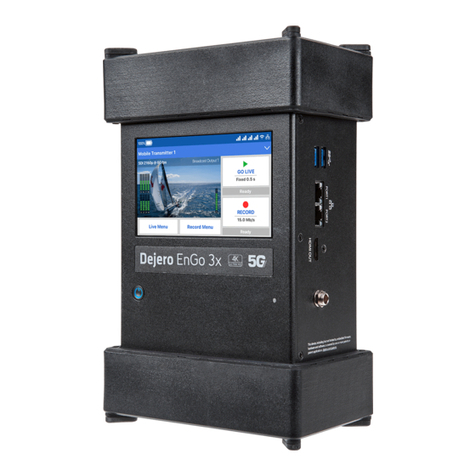
2.1 Test points
STDES-WBC86WTX features several connectors and test points to provide easy access to key signals.
Figure 4. STDES-WBC86WTX test points
Table 1. STDES-WBC86WTX test points
Connector/test point Name Description
P1 Coil connection Transmitter coil connection
AC1_COIL AC1_COIL AC1_COIL signal sensing
AC1 AC1 Resonant circuit terminal
AC2 AC2 Resonant circuit terminal
Vrect Vrect Inverter voltage sensing
Vout Vout Input voltage sensing
VS VS VS signal sensing
5V0 5V0 5 V LDO output
V1V8 V1V8 1.8 V LDO output
GND GND Ground
P3 Digital interface I²C and RST signals
JP1, JP2, JP3 Pull up connection Pull-ups connection for I²C
JP4 Vin selection Input selection
J1 Input voltage USB power input
P2 Input voltage Pin cable power input
TN1442
Test points
TN1442 - Rev 2 page 5/25

2.2 Reference design specifications
The STDES-WBC86WTX target specifications are listed in the table below.
Table 2. STDES-WBC86WTX design specifications
Parameter Description
Tx application PCB area 16 mm x 11 mm
Tx coil specifications Inductance 6.8 µH, DCR 110 mOhm
Dimensions 20.5 mm diameter x 2.8 mm
Input voltage (Vin) 5 V
Input current (Iin) 1 A
Host MCU STM32 used as a reference, the reference I²C driver can be ported to any other
MCU family
Efficiency 58.64% (2.5 W operation) with STDES-WLC38WA
60.23% (peak efficiency) with STDES-WLC38WA at 2 W
Applicable charging gap between Tx
and Rx coils (z-distance)
4.4 mm (2.5 W output) with STDES-WLC38WA receiver, maximum 7 mm – stable
communication without output enabled
Operational modes Transmitter only
TN1442
Reference design specifications
TN1442 - Rev 2 page 6/25

3 Test setup
3.1 Test conditions and equipment
The test setup consists of:
• a power supply (HMP4040 by Rohde & Schwarz)
• a pin power cable
• the STDES-WBC86WTX as a transmitter
• the STDES-WLC38WA as a receiver
• an electronic load in CC mode (BK Precision 8500)
Figure 5. STDES-WBC86WTX and STDES-STWLC38WA test setup
3.2 Test procedure
To achieve the best performance, follow the procedure below.
Step 1. Test the power supply.
The board is powered by voltage supplied by either a USB or a pin cable. This voltage can be
monitored via the VOUT test point. The input voltage also supplies power to the internal 5 and 1.8 V
LDOs. The regulator outputs can be monitored using the appropriate test points. The STDES-
WBC86WTX derives its own power supply directly from the input voltage.
The aim of the test is to check whether the device is powered correctly. The table below shows the
reference range.
Table 3. Internal regulators: output voltage ranges
Item Minimum [V] Typical [V] Maximum [V]
V5V0 3.5 5.0 5.5
V1V8 1.62 1.8 1.98
Step 2. Download the firmware.
The firmware offers all standard functionalities. The device automatically starts in TX mode and starts
pinging after the power-up.
TN1442
Test setup
TN1442 - Rev 2 page 7/25

Step 3. Test the ping functionality.
During pinging, the input current switches between two distinct values periodically. The AC1 and AC2
voltage oscillates with a 5 V amplitude.
Step 4. Test the power transfer start.
Place the receiver onto the transmitter and wait for the status LED indicating an ongoing power transfer
on the receiver to light up. The output should be enabled shortly. A switching waveform can be seen on
the AC1 and AC2 pins.
Step 5. Test the ASK demodulation.
The demodulated signal can be seen on the VS test point. The signal should be clear and carry Qi
encoded packets. This signal is fed to the STWBC86 for communication decoding.
Step 6. Test the efficiency.
Establish the power transfer between the STDES-WBC86WTX and the STDES-WLC38WA. Measure
the input power and output power of the system and calculate the efficiency.
Step 7. Test the thermal performance.
Establish the power transfer and let the system achieve a steady operating temperature. Read the
temperature using either the device internal thermal sensor or a thermal camera.
TN1442
Test procedure
TN1442 - Rev 2 page 8/25

4 Measurements, waveforms, and test data
4.1 Power-up waveform
The figure below shows a startup waveform, from the transmitter perspective.
Figure 6. Start-up sequence of the STWBC86WTX and STWLC38WA
The pinging start can be identified from the AC1 and AC2 waveforms. After registering the power signal, the
receiver initializes communication. When the initial communication is resolved, the receiver enables its output.
The power receiver maintains communication with the transmitter over the course of the power transfer, as it must
provide feedback to ensure a proper regulation.
4.2 ASK packet example
In the figure below, an ASK packet communication example is shown. The VS signal is demodulated from the
power signal.
Figure 7. ASK packet example
The message shown in the figure is a Qi-based CE packet, providing regulation feedback to the transmitter.
TN1442
Measurements, waveforms, and test data
TN1442 - Rev 2 page 9/25

4.3 Typical performance characteristics
The following table shows the charging performance of an STDES-WBC86WTX/STDES-WLC38WA (TX/RX)
setup at various load currents, with the temperature being measured after 5 minutes of continuous operation.
Table 4. STDES-WBC86WTX typical performance
Vin [V] (TX) Iin [mA] (TX) Vout [V] (RX) Iout [mA] (RX)
5,09 263 5,035 100
5,042 382 5,032 200
5,026 502 5,032 300
4,986 670 5,03 400
4,985 860 5,028 500
4.4 Efficiency and spatial freedom
Efficiency is one of the most important metrics of wireless charging performance evaluation. Spatial freedom, the
size of the area for the XY plane in which a power receiver can be placed on the power transmitter, which still
allows sufficient power to be transmitted, is another important metric.
The z-axis distance between the coils, also known as the charging gap, is an additional parameter, which
significantly affects charging performance. Therefore, the STDES-WBC86TX was also tested at various charging
gap distances.
Efficiency and spatial freedom of the STDES-WBC86TX were measured with the STDES-WLC38WA as the
receiver. The efficiency was measured from the transmitter DC input to the receiver DC output. The measurement
does not include any power losses in the wall adapter or the USB cable.
A typical setup is with the fully aligned coils with a 3 mm charging gap (2 mm Tx spacer and 1 mm Rx spacer).
The maximum efficiency achieved with this setup was 60.23%.
Figure 8. Efficiency measurements of the STDES-STWLC38WA and STDES-WBC86TX
The transmitter can deliver 2.5 W even with a 4 mm misalignment in the XY plane or a 4.4 mm charging gap. It is
also able to start communication, with disabled Vout, with up to 7 mm misalignment in the XY plane or distance in
the Z axis.
TN1442
Typical performance characteristics
TN1442 - Rev 2 page 10/25

4.5 Thermal performance
The following figure shows thermal performance of the board with a 2.5 W load (5 V/0.5 A on the Rx side) after 10
minutes of continuous operation.
Figure 9. Thermal performance of the STDES-WBC86WTX at 2.5 W after 10 minutes
Figure 10. Thermal performance of the STDES-WBC86WTX with the STDES-STWLC38WA after 10 minutes
TN1442
Thermal performance
TN1442 - Rev 2 page 11/25

5 Design
5.1 Schematic diagrams
Figure 11. STDES-WBC86WTX circuit schematic (1 of 2)
BOOT2
BOOT1
GND
AGND
12
2u2
C17
12
10u
C13
AGND
V1V8
VIN
V5V0
GPIO0
GPIO1
INTB
SDA
SCL
RSTB
NTC
V1V8
12
10u
C14
12
100n
C15
12
C6 47n
12
C7 47n
2
1
P2
Header 2
12
4u7
C16
SGND
1 2
R4
5k1 SGND
F1 1.5A
21
D5
SMAJ22A-13-F
1 2
180RL1
1
BLM21SP181BH1
2
100n
C22
VIN_F
13
2
JP4
2
4
5
3
1
D
D
V
G
ID
-
+
N
BU
D
S
Shell Shield
J1
NC
D8
C8 NC
E7 BOOT1
AC1
A6
B6 AC1
B7 AC1
AC1
A7
AC2
A2
A3
B2
C1
B3
A
A
A
C
C
C
2
2
2
BOOT2
C7 NC
NC
D7
VSSP
V
V
V
SSP
SSP
SSP
A
A
B1
B8
1
8
VINV A4
VINV A5
NC D1
C3
VINV
VINV
VINV B5
B4
NC E8
C2
NC
VSSA
C5 VSSA
D3 VSSA
D4 VSSA
D5
VSSA
F6
E5 VSSA
VSSA
F5
VSSA
G6 VSSA
G7
VIN D2
VIN E1
VIN E2
VIN E3
H2
GPIO0 H1
GPIO1 J4
GPIO2 J3
GPIO3 J2
GPIO4 J1
GPIO5
J7
INTB
SDA J8
SCL H8
J6
RSTB
J5
GPIO7
DFT
G1
C6
D6
N
N
N
T
C
C
F1 VS
C
F8
F2
VIN
E4
VSSD
VSSD F3
F4
VSSD
VSSD H3
G2
VSSD G3
VSSD
VSSD G4
C4 VSSA
VSSD
H4
VSSD
H5
H7 VSSD
H6 VSSD
V5V0
E6
F7 V5V0
G8
V1V8
G5
V1V8
U1
STWBC86JR
VIN
PGND
AC1
AC2
AC1
AC2
VS
VINV
TN1442
Design
TN1442 - Rev 2 page 12/25

Figure 12. STDES-WBC86WTX circuit schematic (2 of 2)
AGND
21
D1
1N4448HLP
12
10n
C18
12
22n
C20
12
C21
680p
12
10n
C19
1 2
R1
5k1
1 2
R2
220k
1 2
R3
10k
21
N.M.
D2
VS
AC1_COIL
12
C5
AC1
AC1_COIL
AC2
12
C2 100n
12
C3 100n
1
2
P1
6u8
COIL
12
C1 100n
12
C4 47n
VS
V5V0
V1V8
AC2
AC1_COIL
AC1
1
TP1 VINV
VIN
1
TP2
1
TP3
1
TP4
1
TP5
1
TP6
1
TP7
1
TP8
PGND AGND SGND GND
P4
PCB groundpoint
21
D3
1 2
R5
560R
21
D4
SGND
V5V0
GPIO0 GPIO1
HE-RED HE-GRN
C1 6
C2 3
E1
1
4E2
B2 5
B1
2
Q1
ADC114YUQ
SGND
SDA
SCL
INTB
RSTB
VIN_F
V1V8
6
5
4
3
2
1
P3
Header 6
12
JP3
12
JP2
12
JP1
1 2
R8
4k7
1 2
R7
4k7
1 2
R6
4k7
1 2
R9
10k
RSTB
VINV
PGND
12
C9
10u
12
10u
C10
12
10u
C11
12
C12
100n
N.M.
TN1442
Schematic diagrams
TN1442 - Rev 2 page 13/25

5.2 Bill of materials
Table 5. STDES-WBC86WTX bill of materials
Item Q.ty Ref. Part/value Description Manufacturer Order code
1 3 C1, C2, C3 100n C1206
50V 5% MLCC, NP0 Murata GRM31C5C1H104JA01L
2 1 C4 47nF C1206
50V 5% MLCC, NP0 Murata GCM31M5C1H473JA16L
3 2 C6, C7 47n C0402 50V
10% MLCC, X7R Murata GRM155R71H473KE14D
45C9, C10, C11,
C13, C14
10u C0805 35V
10% MLCC, X5R Murata GRM21BR6YA106KE43L
5 2 C12, C15 100n C0402
50V 10% MLCC, X7R Murata GCM155R71H104KE02D
6 1 C17 2u2 C0402 25V
10% MLCC, X5R Murata GRM155R61E225KE11D
7 1 C16 4u7 C0402 10V
20% MLCC, X5R Murata GRM155R61A475MEAAD
8 2 C18, C19 10n C0402 25V
10% MLCC, X5R TDK CGA2B2X5R1E103K050BA
9 1 C20 22n C0402 25V
10% MLCC, X5R TDK C1005X5R1E223K050BA
10 1 C21 680p C0402
25V 5% MLCC, NP0 Murata GRM1555C1E681JA01D
11 1 C22 100n C0603
50V 10% MLCC, X7R Murata GCM188R71H104KA57J
12 1 D1 X1-DFN1006-2 Schottky diode,
80V, 125mA Diodes Inc. 1N4448HLP-7
13 1 D2 SOD-882 2%
5.1V Zener
diode, 250mW
(not mounted)
NXP BZX884-B5V1,315
14 1 D3 D0603 Red LED, high
efficiency Kingbright APHD1608LSURCK
15 1 D4 D0603 Blue LED, high
efficiency Kingbright APHD1608LVBC/D
16 1 D5 SMA_DO-214A
C
uni-directional
TVS 22V Diodes Inc. SMAJ22A-13-F
17 1 F1 F1206 63V 1.5A fuse Littelfuse Inc. 043701.5WR
18 1 J1
Micro USB
female
connector
Wurth
Elektronik 629105150921
19 2 J2, J3 Test point (not
mounted) - -
20 3 JP1, JP2, JP3
Tin-drop
selector (not
mounted)
- -
21 1 JP4 SIL-3
100 mils pitch
pin header,
vertical, 7 mm,
black
Harwin M20-9990345
22 1 L1 180R L0805 4A ferrite bead Murata BLM21SP181BH1
TN1442
Bill of materials
TN1442 - Rev 2 page 14/25

Item Q.ty Ref. Part/value Description Manufacturer Order code
23 1 P1
20 mm diameter
wireless TX coil
(not mounted)(1)
Wurth
Elektronik 760308101104
24 1 P2 SIL-2
100 mils pitch
pin header,
vertical, 7 mm,
black (not
mounted)
Harwin M20-9990246
25 1 P3 SIL-6
100 mils pitch
pin header,
vertical, 7 mm,
black
Harwin M20-9990646
26 1 P4 TH pin, 1.19
mm dia
Probe
grounding pin
Keystone
electronics 4953
27 1 Q1 SOT-363 Dual digital
NPN Diodes Inc. ADC114YUQ-7
28 1 R1 5k1 R0402 1% Resistor YAGEO RT0402FRE075K1L
29 1 R2 220k R0402 1% Resistor YAGEO RT0402FRE07220KL
30 2 R3 10k R0402 1% Resistor YAGEO RT0402FRE1310KL
31 1 R4 5k1 R0603 1% Resistor YAGEO RT0603FRE075K1L
32 1 R5 560R R0603
5% Resistor YAGEO RT0603FRE07560RL
33 3 R6, R7, R8 4k7 R0603 5% Resistor YAGEO RT0603FRE074K7L
34 1 Jumper for JP4 2,54mm JUMP-
SW 2,54mm Jumper Wurth
Elektronik 60900213421
35 8
TP1, TP2, TP3,
TP4, TP5, TP6,
TP7, TP8
1.02mm hole,
white
TH ring test
point (not
mounted)
Keystone
electronics 5001
36 1 U1 STWBC86JR
Qi-compatible
inductive
wireless power
transmitter for
up to 5 W
applications
ST STWBC86JR
37 1 R9 10k R0603 5% Resistor YAGEO RT0603FRE0710KL
38 1 pair plexi - 30x30x3.8mm
2mm milling Any Any
39 4 screws -
10mm length
5.5mm head
diameter M3
(countersunk
head)
Any Any
40 4 standoff - 6x5.5 M3 Keystone
Electronics 25508
41 1 bumper - 9.8x8x6mm M3 SJ61A2
1. The terminals of the coil must be cut to the length and soldered to P1 after the coil has been correctly positioned by using
the plastic supports. Do not use glue or adhesive tape.
TN1442
Bill of materials
TN1442 - Rev 2 page 15/25

5.3 PCB layout
Figure 13. STDES-WBC86WTX top layer
Figure 14. STDES-WBC86WTX inner1 layer
Figure 15. STDES-WBC86WTX inner2 layer
TN1442
PCB layout
TN1442 - Rev 2 page 16/25

Figure 16. STDES-WBC86WTX bottom layer
TN1442
PCB layout
TN1442 - Rev 2 page 17/25

6 STDES-WBC86WTX default configuration
Basic parameters:
Table 6. STDES-WBC86WTX default configuration: basic parameters
Parameter Value
Tx bridge mode Full sync
Minimum duty cycle 10%
Maximum duty cycle 50%
Minimum operating frequency 110 kHz
Maximum operating frequency 148 kHz
Ping duty cycle 50 %
Ping frequency 146 kHz
Ping duration 80 ms
Ping interval 2,000 ms
Over-current protection (OCP) 2 A
Over-voltage protection (OVP) 20 V
Over-temperature protection (OVTP) 100°C
PID maximum current Unlimited
Maximum CEP timeout count (for fhop feature) 3
Fhop step 1,920 kHz
Protection debounce 0
• Enabled interrupts:
– Bridge mode change
– CEP timeout
– RPP timeout
– Packet sent successfully
– EPT from RX received
– OCP triggered
– OVP triggered
– OVTP triggered
• Enabled features:
– auto ping
– fhop
– duty cycle regulation
• EPT conditions after which the device does not start pinging automatically:
– OVP triggered
– System error
• GPIOs:
– No functions assigned
TN1442
STDES-WBC86WTX default configuration
TN1442 - Rev 2 page 18/25

7 Conclusions
The test results show the STDES-WBC86WTX reference design is capable of transmitting up to 2.5 W of power,
while also:
- achieving system efficiency of up to 60.23% with the STDES-WLC38WA,
- maintaining chip temperature below 65°C after 10 minutes of continuous 2.5 W transmission operation,
- and ensuring a robust ASK demodulation for a reliable communication with the power receiver.
The STDES-WBC86WTX reference design achieved the expected performance.
TN1442
Conclusions
TN1442 - Rev 2 page 19/25

Appendix A Reference design warnings, restrictions and disclaimer
Important: The reference design is not a complete product. It is intended exclusively for evaluation in laboratory/
development environments by technically qualified electronics experts who are familiar with the dangers and
application risks associated with handling electrical/mechanical components, systems and subsystems.
Danger: Exceeding the specified reference design ratings (including but not limited to input and
output voltage, current, power, and environmental ranges) may cause property damage,
personal injury or death. If there are questions concerning these ratings, contact an
STMicroelectronics field representative prior to connecting interface electronics, including
input power and intended loads. Any loads applied outside of the specified output range
may result in unintended and/or inaccurate operation and/or possible permanent damage to
the reference design and/or interface electronics. During normal operation, some circuit
components may reach very high temperatures. These components include but are not
limited to linear regulators, switching transistors, pass transistors, and current sense
resistors which can be identified in the reference design schematic diagrams.
STMicroelectronics reference designs are solely intended to assist designers ("buyers") who are developing
systems that incorporate STMicroelectronics semiconductor products (herein, also referred to as "components").
The buyer understands and agrees that he/she is the only responsible for independent analysis, evaluation and
judgment in designing his/her own systems and products. STMicroelectronics has conducted only the
measurements and tests specifically described in the published documentation for the specified reference design.
STMicroelectronics may correct, enhance, improve its reference designs for future development.
STMicroelectronics reference designs are provided "as is". STMicroelectronics does not promise that reference
designs are accurate or error free. STMicroelectronics makes no warranties or representations with regard to the
reference designs or use of the reference designs, express, implied or statutory, and specifically disclaims all
warranties, express or implied, as to the accuracy or completeness of the information contained therein.
STMicroelectronics disclaims any warranty of title and any implied warranties of merchantability, fitness for a
particular purpose and non-infringement of any third-party intellectual property rights concerning
STMicroelectronics reference designs or their use. STMicroelectronics shall not be liable for and shall not defend
or indemnify buyers against third-party infringement claim that relates to or is based on a combination of
components provided in an STMicroelectronics reference design.
In no event shall STMicroelectronics be liable for any actual, special, incidental, consequential or indirect
damages, however caused, on any theory of liability and whether or not STMicroelectronics has been advised of
the possibility of such damages, arising in any way out of STMicroelectronics reference designs or buyer's use of
STMicroelectronics reference designs.
You further acknowledge and agree that the reference designs may not be used in or in connection with any legal
or administrative proceeding in any court, arbitration, agency, commission or other tribunal or in connection with
any action, cause of action, litigation, claim, allegation, demand or dispute of any kind.
TN1442
Reference design warnings, restrictions and disclaimer
TN1442 - Rev 2 page 20/25
Table of contents