Standart HX290UKA User manual

Hand held Transceiver
HX290U(KA)
SERVICE MANUAL
Copyright © 1999
Marantz Japan, Inc
All Rights Reserved
Printed in Japan
HX290UKA131 / 191 / 181 / 111

1
CONTENTS
1. CONTROLS AND CONNECTIONS..........................................................................................................................................2
2. THEORY OF OPERATIONS.....................................................................................................................................................3
2.1 PLL Block ...........................................................................................................................................................................3
2.2 Receiver Block ...................................................................................................................................................................4
2.3 Transmitter Block ..............................................................................................................................................................6
2.4 Control Block .....................................................................................................................................................................7
2.5 Power Supply Block ........................................................................................................................................................10
3. DISASSEMBLY ......................................................................................................................................................................11
3.1 Removing the Diecast frame ..........................................................................................................................................11
3.2 Removing the TX/RX/CONTROL P.C.board...................................................................................................................12
4. ADJUSTMENT........................................................................................................................................................................13
4.1 Adjustment Connection Diagrams.................................................................................................................................16
4.2 Adjustment Point Diagrams............................................................................................................................................17
4.3 HX290UKA Adjustment and Confirmation ....................................................................................................................18
4.3.1 PLL Block ................................................................................................................................................................18
4.3.2 Transmitter Block ...................................................................................................................................................18
4.3.3 Receiver Block ........................................................................................................................................................19
5. SPECIFICATIONS ..................................................................................................................................................................21
6. PARTS LIST ...........................................................................................................................................................................22
7. EXPLODED PARTS VIEW .....................................................................................................................................................30
8. PACKING DIAGRAM AND PARTS LIST...............................................................................................................................31
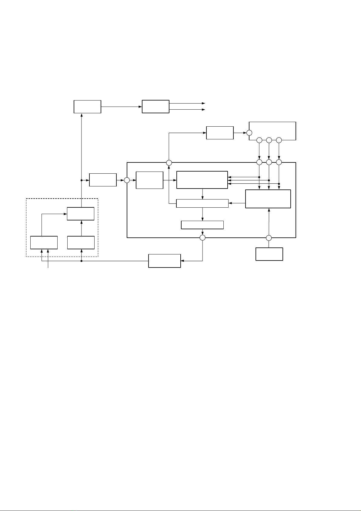
9. BLOCK DIAGRAM .................................................................................................................................................................32
10. SCHEMATIC DIAGRAM ........................................................................................................................................................33
10.1 HX290UKA131 ................................................................................................................................................................33
10.2 HX290UKA191 ................................................................................................................................................................34
10.3 HX290UKA181 ................................................................................................................................................................35
10.4 HX290UKA111 ................................................................................................................................................................36
11. COMPONENT OVERLAY DIAGRAM ....................................................................................................................................37
This service manual is for use with the HX290UKA131/191/181/111 transceiver.
The HX290UKA131 is a transceiver for use with the 450MHz to 470 MHz.
The HX290UKA191 is a transceiver for use with the 370MHz to 390 MHz.
The HX290UKA181 is a transceiver for use with the 345MHz to 370 MHz.
The HX290UKA111 is a transceiver for use with the 405MHz to 430 MHz.
• Accessories
HX290 Transceiver
Flexible antenna
Beltclip
Owner's manual
•Options
CNB290 : Ni-Cd battery pack (7.2 V 1100 mAh)
CNB291 : Ni-Cd battery pack (7.2 V 1500 mAh)
CSA290 : Charger
CSA291 : Rapid charger

2
1. CONTROLS AND CONNECTIONS
qq(power / volume) knob
wwCH (channel) knob
eeTX/BUSY Indicator
rrAntenna connector
ttPTT switch
yyMONITOR key
uuLAMP key
iiSCN (scan) key
ooDIAL key
!!00 T/A (Talkaround) key
!!11 H/L (high/low) key
!!22 Keypad
Figure 1-1
CH
TX/BUSY
HX290
SCN
123A
456B
789C
0#D
DIAL T/A H/L
Monitor indicator Scan indicator Voice scrambler
indicator
Low power
indicator
Channel
indicator
Talkaround
indicator
Keylock
indicator
Figure 1-2

3
2. THEORY OF OPERATIONS
Note : Refer to the block diagrams (figure 2-1 through 2-8) in the text for the operations of the circuits.
2.1 PLL Block
The PLL block comprises a VCO, TCXO, PLL IC, and PLL loop filter.
The VCO circuit generates the transmission signal and first local signal directly.
2.1.1 Programmable Divider
The input oscillation signal is frequency divided by the
prescaler using a determined division ratio (1/64 or 1/65).
After this, the oscillation signal is input to a programmable
divider built into the PLL IC. Based on the data from
microprocessor QL02, the programmable divider
frequency divides the oscillation signal from the VCO to
1/N to generate a comparison frequency (fp) of 5 kHz or
6.25 kHz.
2.1.2 Reference Divider
The reference divider is a circuit that generates a
reference frequency (fr) of 5 kHz or 6.25 kHz based on
data from microprocessor QL02. The 12.8 MHz reference
oscillation signal from the TCXO passes through pin 1 of
PLL IC QP02 and is input to the reference divider built
into the PLL IC.
The 12.8 MHz reference oscillation signal is frequency
divided to 1/2,560 (1/2,048) to generate a reference
frequency of 5(6.25) kHz.
2.1.3 Phase Comparator
The phase comparator compares the comparison
frequency (fp) and the reference frequency (fr) to
determine the phase difference.
2.1.4 Charge Pump
The charge pump circuit charges and discharges the
electrical charge accumulated in the PLL loop filter.
2.1.5 PLL loop Filter
The PLL loop filter CR integrates the level signal (square
wave) output from the charge pump, converting it into a
DC voltage.
1/N
PLL loop filter
Audio signal
TCXO
8
Charge pump
Phase comparator
51
14 9 10 11
QP04
DTC114YE
(fr)
(fp)
PLL IC
Unlock
5 kHz
(6.25 kHz)
5 kHz
(6.25 kHz)
QP02 - MB15E03
QL02
81 82 77
28
Strobe
Data
Clock
1/2560
(1/2048)
Reference divider
Programmable divider
Prescaler
Microprocessor
Unlock switch
12.8 MHz
2SC5005
QV07
VCO buffer amplifier
DAN235E
QP09
TX/RX switch
Transmission signal (TX)
First local signal (RX)
2SC5005
QP08
(0 dB amp)
Buffer amplifier
Approx. 300 mV
XP01
2SK1875(V)
QV06
VCO RX
2SK1875(V)
QV04
VCO TX
VCO
2SC4726
QP10
Buffer amplifier
Figure 2-1 PLL block diagram

4
2.1.6 VCO Circuit
The DC voltage output by the PLL loop filter is input to a
variable capacitance diode built into the VCO. This DC
voltage changes the capacitance between the electrodes
of the variable capacitance diode, thereby controlling the
oscillation signal of the VCO.
2.1.7 Unlock Detect Circuit
The microprocessor QL02 (pin 37) determines whether
the status of the PLL circuitry is lock or unlock according
to the output level (high or low) from pin 14 of the PLL IC.
If the phase comparator built into the PLL IC detects no
phase difference (PLL circuit locked), it produces a high
level output. This high level output signal is input to an
unlock switch QP04, causing it to turn on. When the
unlock switch is on, a low level output signal is input to pin
37 of microprocessor QL02. The low level input causes
microprocessor QL02 to determine that the PLL circuit is
locked.
If there is a phase difference (PLL circuit unlocked), the
phase comparator produces a low level output. This low
level output signal is input the unlock switch QP04,
causing it to turn off. When the unlock switch is off, a high
level output signal is input to pin 37 of microprocessor
QL02. The high level input causes microprocessor QL02
to determine that the PLL circuit is unlocked.
2.2 Receiver Block
The reception method is double-conversion superheterodyne with a first IF frequency of 44.95 MHz (Lower) and a second IF
frequency of 455 kHz (Lower). The receiver block comprises an RF amplifier circuit, first mixer circuit, first IF amplifier circuit,
second IF circuit, and audio circuit.
QH04
TA31136FN
Antenna switch RF amplifier
First IF amplifier
Second IF IC
Crystal filter First mixer
QT04-HVU131
QT05-HSC277
16
B.P.F. QF02
2SK274
QF03
SGM2014AM
FH01
First local signal (Approx. 300 mV)
(20 dB amp)
(20 dB amp)
L.P.F.
B.P.F.
QH03-2SC4649
Audio signal
Figure 2-2 Receiver block diagram
2.2.1 RF Amplifier Circuit
The reception frequency amplified by approximately 20 dB
by RF amplifier QF02, after which it is input to a band-pass
filter consisting of LF04, CF11, CF29, CF13, LF05, CF14,
CF15, LF06, CF16, CF17, CF18, LF07, CF19(only
HX290UKA131/181/111) and CF20. At this point, unwanted
frequency elements removed by the band-pass filter.
2.2.2 First Mixer Circuit
The reception frequency (frX) is mixed with the first local
signal (fvco) from the VCO by first mixer QF03, and first
IF signals consisting of their difference are generated.
frx - fvco = 44.95 (MHz)
frx : Reception frequency
fvco : First local signal
2.2.3 First IF Amplifier Circuit
Bandwidth of crystal filter FH01 depends on setting of
channel separation.
After being amplified by approximately 20 dB by first IF
amplifier QH03, the 44.95 MHz first IF signal is input to
pin 16 of second IF IC QH04.

5
2.2.4 Second IF Circuit
The second IF IC comprises a second local oscillator,
second mixer, second IF amplifier, wave detector, noise
amplifier, and noise wave detector.
The first IF signal passes through pin 16 of second IF IC
QH04 and is input to the second mixer built into QH04.
The first IF signal and second local signal are mixed, and
the first IF signal is converted into a 455 kHz second IF
signal. After having adjacent signal elements eliminated
by ceramic filter FH05 (6 dB bandwidth ±6.0 kHz or
greater), the second IF signal is converted into an audio
signal by the second IF amplifier and a quadrature wave
detector.
9 8
53
32
12 14
QM01 QA01
TA7368F
Second IF IC
QH04
TA31136FN
De-emphasis circuit
CH23, RH14, CH21, RH22
CH22, RH12, RH13, CH30
Band pass filter
audio signal
First IF signal
First IF amplifier
squelch signal
Quadrature wave
detector
1
Second
mixer
Second local
oscillator
Crystal
resonator Ceramic filter
(6dB bandwidth ±6 kHz or greater)
Second local signal
(44.495 MHz)
Second IF
amplifier
Noise
amplifier
Noise wave
detector
Microprocessor
AF power amplifier
16
XH01
44.495 MHz FH05
455 kHz QL02
QH03-2SC4649
Inverter
amplifier
(Approx. 6 dB amp)
Figure 2-3 Second IF circuit block diagram
2.2.5 Audio Circuit
The frequency of a portion of the audio signal is corrected
by the de-emphasis circuit built into base band IC QM01.
After this, the audio signal is amplified by approximately 6
dB by AF amplifier built into QM01. After passing through
AF mute switch QM02, the audio signal is input to pin 4 of
AF power amplifier QA01.
The audio signal is amplified to approximately 0.5 W by
QA01.
RA01
volume
14
65 32
10
Second IF IC
0.5W
Speaker
EL01
Ext. speaker jack
3.5 DIA.
JA01
4
Base band IC AF power amplifier
Audio signal
Squelch signal
Microprocessor
AF mute switch
QM01
AK2342A
QL02 QH04
TA31136FN
QA01
TA7368F
ON
OFF
OFF
ON
QL02 QM02 Squelch operation
Pin 65 Hi output
Pin 65 Lo output
QM02
HN1K02FU
(Approx. 6 dB amp)
Figure 2-4 Audio circuit block diagram

6
2.2.6 Squelch Circuit
A portion of the audio signal output from pin 9 of second
IF IC QH04 is input to a band-pass filter consisting of
CH23, RH22,CH30,RH14, CH21, CH22, RH12 and
RH13. Noise elements are extracted from the audio signal
by the band-pass filter and input to pin 8 of QH04 as the
noise signal. The noise signal has approximately 40 kHz
elements only amplified by a noise amplifier built into
QH04 to generate the squelch signal. This squelch signal
is converted into a DC signal by the noise wave detector
built into QH04 and then output from pin 14 of QH04.
Refer to figure 2-4 for a description of the squelch on and
off operation.
2.2.7 Tone Decoder
A portion of the audio signal output from pin 9 of second
IF IC QH04 is input to tone detector circuit built into base
band IC QM01 as the tone signal.
At this point, if the QM01 detects a match between the
input tone signal and the transceiver's tone signal setting,
output signals from pins 22 of QM01 is input to pin 69 of
microprocessor QL02. And the high level signal is output
from pin 65 and 66 of QL02. (Refer to figure 2-4) The high
level signal is input to AF mute switch QM02, causing it to
turn on. This causes an audio signal to be output from
internal speaker EL01.
2.3 Transmitter Block
2.3.1 Microphone Amplifier
Audio signal is input to the microphone amplifier built into base band IC QM01 and amplified by approximately 47 dB. QM01
has a built-in pre-emphasis circuit (6 dB/oct frequency characteristics), and the high-frequency components of the audio
signal are boosted and modulated. Also, the frequency elements 3 kHz and above are eliminated by low-pass filter built into
QM01 to limit the bandwidth. Refer to figure 2-5 for a description of the microphone mute switch QM09 operation.
(Approx. 47 dB amp)
(6 dB/oct)
8 2
73
Microphone
NL01
Base band IC
Audio signal
PTT switch
Microprocessor
QV04
2SK1875(V)
QL02
QM01
AK2342A
VCO TX
ON
OFF
QL02 Microphone mute
Pin 73 Hi output
Pin 73 Lo output
Mic mute switch
QM09
2SK1830
Figure 2-5 Microphone amplifier circuit block diagram
2.3.2 Pre-amplifier / Power amplifier
Refer to figure 2-6 for a description of circuit operation.
Pre-amplifier QT01, QT02 amplify the approximately 1
mW transmission signal by 17 dB to approximately 50
mW. The transmission signal is further amplified by
approximately 4 W by the power amplifier QT03.
2.3.3 Tone Encoder
Serial data output from pins 78, 81, 82 of microprocessor
QL02 is input to the base band IC QM01. QM01 then
outputs the tone signal specified by the serial data from
the microprocessor.
Antenna switch
QT04-HVU131
QT05-HSC277
L.P.F.
PLL buffer amplifier
QP08
2SC5005
TX/RX switch
QP09
DAN235E
Pre-amplifier
QT01-2SC5005
(19 dB amp)
(17 dB amp)
(0 dB amp)
4 W
VCO TX
QV04
Power amplifier
QT03
MODEL QT03
HX290UKA131 M68732(HM)
HX290UKA191 M68732(UL)
HX290UKA181 M68732(SL)
HX290UKA111 M68732(L)
1 mW 50 mW
VCO buffer amplifier
QV07
2SC5005
(0 dB amp)
0 dBm 1 mW 1 mW QT02-2SC5227
Figure 2-6 Transmission circuit block diagram

Function
LCD segment output
LCD segment output
LCD segment output
LCD segment output
Ground
LCD segment output
LCD segment output
LCD segment output
LCD segment output
LCD segment output
LCD segment output
LCD segment output
LCD segment output
LCD segment output
LCD segment output
LCD segment output
LCD segment output
LCD segment output
LCD segment output
LCD segment output
Key Matrix output
Key Matrix output
Key Matrix output
Key Matrix output
Key Matrix input
Key Matrix input
Key Matrix input
Key Matrix input
A/D reference voltage
A/D converter power supply
Key Matrix input
Squelch level detect
Battery voltage down detect
EEPROM clock
EEPROM data
Wide/Narrow switch (Hi:Narrow)
Unlock detect (Hi:Unlock)
SmarTrunk connection detect
A/D converter ground
Rotary encoder turn detect (interrupt)
Rotary encoder turn direction detect
DCS reception detect (interrupt)
Not used
Not used
LCD backlight
Power down detect (interrupt)
Power supply terminal (+5 V)
DTMF IC power save mode setting output
P.UP/DN
---
---
---
---
---
---
---
---
---
---
---
---
---
---
---
---
---
---
---
---
E-UP
E-UP
E-UP
E-UP
E-DN
E-DN
E-DN
E-DN
---
---
E-DN
---
---
---
---
---
---
I-UP
---
E-UP
E-UP
---
E-UP
E-UP
E-UP
---
---
---
Initial
---
---
---
---
---
---
---
---
---
---
---
---
---
---
---
---
---
---
---
---
High
High
High
High
(Low)
(Low)
(Low)
(Low)
---
---
(Low)
(High)
(High)
Low
Low
---
Low
(High)
---
(---)
(---)
(---)
(---)
Low
Low
(High)
---
High
Active
---
---
---
---
---
---
---
---
---
---
---
---
---
---
---
---
---
---
---
---
---
---
---
---
High
High
High
High
---
---
High
Low
Low
---
---
---
High
Low
---
---
---
Low
---
High
Low
---
High
In/Out
O
O
O
O
-
O
O
O
O
O
O
O
O
O
O
O
O
O
O
O
O
O
O
O
I
I
I
I
-
-
I
A/D
A/D
O
I/O
O
I
I
-
INT
I
INT
I
O
O
INT
-
O
Signal Name
SEG05
SEG06
SEG07
SEG08
Vss
SEG09
SEG10
SEG11
SEG12
SEG13
SEG14
SEG15
SEG16
SEG17
SEG18
SEG19
SEG20
SEG21
SEG22
SEG23
KEYO
KEYO1
KEYO2
KEYO3
KEYi
KEYi1
KEYi2
KEYi3
AVR
AVcc
KEYi4
SQL
LO BATT
EE CLK
EE DAT
W/N
U/L
TRUNK CHK
AVss
ROT INT
ROT TURN
DCS INT
ROT 2
---
ROT3 LAMP
P DOWN INT
Vcc2
DTMF PD
S.PD
---
---
---
N-OD
---
N-OD
N-OD
N-OD
N-OD
N-OD
N-OD
N-OD
N-OD
N-OD
N-OD
N-OD
N-OD
N-OD
N-OD
N-OD
N-OD
N-OD
N-OD
N-OD
N-OD
N-OD
N-OD
N-OD
---
---
CMOS
CMOS
CMOS
CMOS
CMOS
CMOS
CMOS
CMOS
---
CMOS
CMOS
CMOS
CMOS
CMOS
CMOS
CMOS
---
CMOS
S.I/O
O
O
O
I/O
sys
I/O
I/O
I/O
I/O
I/O
I/O
I/O
I/O
I/O
I/O
I/O
I/O
I/O
I/O
I/O
I/O
I/O
I/O
I/O
I/O
I/O
I/O
I/O
sys
sys
I/O
I/O
I/O
I/O
I/O
I/O
I/O
I/O
sys
I/O,INT
I/O,INT
I/O,INT
I/O,INT
I/O,INT
I/O,INT
I/O,INT
sys
I/O,INT
Port Name
SEG05
SEG06
SEG07
P50/SEG08
Vss
P51/SEG09
P52/SEG10
P53/SEG11
P54/SEG12
P55/SEG13
P56/SEG14
P57/SEG15
P60/SEG16
P61/SEG17
P62/SEG18
P63/SEG19
P64/SEG20
P65/SEG21
P66/SEG22
P67/SEG23
P70/SEG24
P71/SEG25
P72/SEG26
P73/SEG27
P74/SEG28
P75/SEG29
P76/SEG30
P77/SEG31
AVR
AVcc
P07/AN7
P06/AN6
P05/AN5
P04/AN4
P03/AN3
P02/AN2
P01/AN1
P00/AN0
AVss
P17/INT17
P16/INT16
P15/INT15
P14/INT14
P13/INT13
P12/INT12
P11/INT11
Vcc2
P10/INT10
No.
1
2
3
4
5
6
7
8
9
10
11
12
13
14
15
16
17
18
19
20
21
22
23
24
25
26
27
28
29
30
31
32
33
34
35
36
37
38
39
40
41
42
43
44
45
46
47
48
7
2.4 Control Block
2.4.1 Microprocessor QL02
The functions of the In / Out ports of microprocessor QL02 are listed below. Table 2-1

Initial
(High)
---
---
---
---
---
Low
---
---
Low
(High)
(High)
(Low)
Low
Low
High
Low
Low
Low
Low
(High)
Low
Low
---
Low
(Low)
(High)
(High)
Low
Low
Low
Low
Low
Low
(Low)
Low
---
---
---
---
---
---
---
---
---
---
---
---
---
---
---
---
P.UP/DN
E-UP
---
---
---
---
---
---
---
---
---
---
---
---
---
---
---
---
---
---
E-UP
E-UP
---
---
---
---
---
I-UP
I-UP
---
---
---
---
---
---
---
E-UP
---
---
---
---
---
---
---
---
---
---
---
---
---
---
---
---
Function
Reset input
Sub clock connection terminal (N.C.)
Sub clock connection (N.C.)
Operation mode specified (Vss)
Main clock connection (9.8304 MHz)
Main clock shift output
Ground
DTMF signal detect signal input
DTMF reception data receipt clock output
DTMF reception data input
SmarTrunk data input (UART)
SmarTrunk data output (UART)
TX+B output
PLL+B output
RX+B output
AF pre-amplifier power supply output
AF main amplifier power supply output
Non connect
DCS output
CTCSS signal detect signal input
DTMF signal output (Low side)
DTMF signal output (High side)
D/A reference voltage
Mic mute setting output
PTT switch detect
MONI key detect
LAMP key detect
PLL strobe output
AK2342 strobe output
SmarTrunk reset output
Transmission power control output (PWM)
Serial clock output
Serial data output (UART data output)
UART data input
BUSY LED light control
LCD boosting circuit capacity connection (N.C.)
Power supply for driving LCD
LCD common output
LCD common output
LCD common output (N.C.)
LCD segment output
LCD segment output
LCD segment output
Power supply (+3 V)
LCD segment output
LCD segment output
Active
Low
---
---
---
---
---
High
---
High
---
---
---
---
High
High
Low
High
High
---
---
Low
---
---
---
High
High
Low
Low
---
---
---
---
---
---
---
Hi-Z
---
---
---
---
---
---
---
---
---
---
---
---
---
---
---
---
In/Out
I
-
-
I
I
O
O
-
I
O
I
O
O
O
O
O
O
O
O
O
I
O
O
-
O
I
I
I
O
O
O
O
O
O
I
O
-
-
-
-
-
-
O
O
-
-
O
O
O
-
O
O
Signal Name
RESET
N.C.
N.C.
Vss
X0
X1
CLK SHIFT
Vss
DTMF STD
DTMF ACK
DTMF SD
S/TRUNK RXD
S/TRUNK TXD
TX
PLL
RX
AF PRE
AF MAIN
---
DCS ENC
CTCSS DEC
DTMF (Lo)
DTMF (Hi)
DVR
MIC MUTE
PTT
MONI
LAMP
PLL STB
AK2342 STB
S/TRUNK RST
TX HI/LO
CLK
DATA (TXD)
RXD
BUSY LED
N.C.
N.C.
V0
V1
V2
V3
COM0
COM1
N.C.
N.C.
SEG00
SEG01
SEG02
Vcc1
SEG03
SEG04
S.PD
---
---
---
---
---
---
CMOS
---
CMOS
CMOS
CMOS
CMOS
CMOS
CMOS
CMOS
CMOS
CMOS
CMOS
CMOS
N-OD
N-OD
D/A
D/A
---
CMOS
CMOS
CMOS
CMOS
CMOS
CMOS
CMOS
CMOS
CMOS
CMOS
N-OD
N-OD
---
---
---
---
---
---
---
---
---
---
---
---
---
---
---
---
S.I/O
sys
sys
sys
sys
sys
sys
I/O
sys
I/O
I/O
I/O
I/O
I/O
I/O
I/O
I/O
I/O
I/O
I/O
I/O
I/O
O
O
sys
I/O
I/O
I/O
I/O
I/O
I/O
I/O
I/O
I/O
I/O
I/O
I/O
sys
sys
sys
sys
sys
sys
O
O
O
O
O
O
O
sys
O
O
Port Name
RSTX
X0A
X1A
MODA
X0
X1
P80/INT24
Vss
P81/INT25
P82/INT26
P83/INT27
P20/UI
P21/UO
P22/UCK
P23/PPG1
P24/INT20
P25/INT21
P26/INT22
P27/INT23
P30
P31
DAOUT2
DAOUT1
DVR
P84/TO21
P85/TO22
P86/EC2/LCLK
P87/EC3
P40/TO11/WTO
P41/TO12/HCLK
P42/PWM1/EC1
P43/PWM2
P44/SCK
P45/SO
P46/SI
P47/PWC
C1
C0
V0
V1
V2
V3
COM0
COM1
COM2
COM3
SEG00
SEG01
SEG02
Vcc1
SEG03
SEG04
No.
49
50
51
52
53
54
55
56
57
58
59
60
61
62
63
64
65
66
67
68
69
70
71
72
73
74
75
76
77
78
79
80
81
82
83
84
85
86
87
88
89
90
91
92
93
94
95
96
97
98
99
100
8

9
2.4.2 Display (LCD)
Microprocessor QL02 drives LCD QL01 directly. The driving method is dynamic drive using 24 segment terminals, two
common terminals, and a 1/3 duty ratio. The LCD segment and common connections are illustrated below.(Figure2-7)
COM0
COM1
SEG0
SEG1
SEG2
SEG3
SEG4
SEG5
SEG6
SEG7
SEG8
SEG9
SEG10
SEG11
SEG12
SEG13
SEG14
SEG15
SEG16
SEG17
SEG18
SEG19
SEG20
SEG21
SEG22
SEG23
COM0
COM1
COMMON
SEGMENT
Figure 2-7 LCD connection diagram

10
Figure 2-8 Power supply circuit block diagram
5V regulator
Battery terminal
DC 7.2 V
PLL 3V switch
QL18
QL02 pin 47,30
QM01 pin 13
QL10 pin10
QL12 pin8
3V regulator
QL19
S81230SG
3 V
Vcc (7.2 V)
5 V
QL06, QP09
QT01, QT02
QT11
QL05, QL03
QA02
QT03 pin 3
QT07 pin 8
Common 5V regulator
Fuse
FA01
Power switch
RA01
QL17
S81350HG
QL07
UMC5N
TX 5V regulator
QL20 - FP208
QL21 - UMG3N
RX switch
QL26
DTA114YE
QL02 pin 98
QP02 pin 4
PLL 3 V
QL20 - FP208
QL24 - UMG3N
TX 5 V
5 V QP04, QP05
QP08, XP01
QP02 pin 3
QP07, QH03,
QH05
QH04 pin 4
QF02, QF03
FH01 pin 3
RX 5 V
2.5 Power Supply Block
The power supply block is diagrammed below.(Figure2-8)

11
3. DISASSEMBLY
Note : Be sure to switch off the transceiver's power before
disassembling it. And then remove an antenna and
a battery pack.
3.1 Removing the Diecast frame
(a) Remove the single screw Ato remove the Mic/Spk
jack cover.
(b) Remove the single nut B, and remove the power/volume
and channel knobs.
(c) Remove the two screws C.
Figure 3-1
Power/volume knob
Channel knob
B
Antenna ring
A
Mic/Spk
jack cover
C
(d) Pull the diecast frame up from front case in the
direction indicated by arrow q, and remove the it in
the direction indicated by arrow w.
Figure 3-2
Diecast
frame
Front case
2
1

12
3.2 Removing the TX/RX/CONTROL P.C.board
(a) Remove the frame packing.
(b) Remove the two nuts D.
(c) Remove the solder from area eon the TX/RX/CONTROL
P.C.board.
Figure 3-3
D
TX/RX/CONTROL
P.C.board
Solder iron
Frame packing
3
(d) Remove the two screws Eto remove the switching
plate and two clampers.
(e) Remove the three screws F. The TX/RX/CONTROL
P.C.board can now be removed.
Switching
plate
Clamper
Diecast frame
TX/RX/CONTROL
P.C.board
E
E
F
Clamper
Figure 3-4

TX/RX adjustment frequencies
–HX290UKA131 –Table 4-1
Channel RX frequency (Wide/Narrow) TX frequency (Wide/Narrow) Tone TX power
00 450.025 MHz (W) 450.100 MHz (W) None Hi
01 460.025 MHz (W) 460.100 MHz (W) None Hi
02 470.025 MHz (W) 470.100 MHz (W) None Hi
03 450.0125 MHz (N) 450.100 MHz (N) None Hi
04 460.0125 MHz (N) 460.100 MHz (N) None Hi
05 470.0125 MHz (N) 470.100 MHz (N) None Hi
06 460.025 MHz (W) 460.100 MHz (W) CTCSS 123 Hi
07 460.0125 MHz (N) 460.100 MHz (N) CTCSS 123 Hi
08 460.025 MHz (W) 460.100 MHz (W) DCS 023 Hi
09 460.0125 MHz (N) 460.125 MHz (N) DCS 023 Hi
13
4. ADJUSTMENT
Make sure that all test equipment is properly calibrated. Allow sufficient time after powering on equipment for it to warm up
before performing adjustments.
- Standard conditions -
Power supply voltage ............................................................................................................................................DC 7.2 V
Audio output ...........................................................................................................................................................200 mW
Audio load ......................................................................................................................................................................8 Ω
Transmission load........................................................................................................................................................50 Ω
Standard modulation frequency..................................................................................................................................1 kHz
Standard frequency deviation.....................................................................................± 3 kHz (Wide) / ± 1.5 kHz (Narrow)
Maximum deviation.....................................................................................................± 5 kHz (Wide) / ± 2.5 kHz (Narrow)
Channel space..............................................................................................................25 kHz (Wide) / 12.5 kHz (Narrow)
Adjustment frequencies.................................................................................................................................See Table 4-1
Note : When performing adjustments, make the channel data settings listed in Table 4-1 in the transceiver. If you need to make
channel data settings, refer to the separate Programming Manual (part number : 408B851040) for details.
–HX290UKA191 –Table 4-2
Channel RX frequency (Wide/Narrow) TX frequency (Wide/Narrow) Tone TX power
00 370.025 MHz (W) 370.100 MHz (W) None Hi
01 380.025 MHz (W) 380.100 MHz (W) None Hi
02 390.025 MHz (W) 390.100 MHz (W) None Hi
03 370.0125 MHz (N) 370.100 MHz (N) None Hi
04 380.0125 MHz (N) 380.100 MHz (N) None Hi
05 390.0125 MHz (N) 390.100 MHz (N) None Hi
06 380.025 MHz (W) 380.100 MHz (W) CTCSS 123 Hi
07 380.0125 MHz (N) 380.100 MHz (N) CTCSS 123 Hi
08 380.025 MHz (W) 380.100 MHz (W) DCS 023 Hi
09 380.0125 MHz (N) 380.100 MHz (N) DCS 023 Hi

TX/RX adjustment frequencies
–HX290UKA181 –Table 4-3
Channel RX frequency (Wide/Narrow) TX frequency (Wide/Narrow) Tone TX power
00 345.025 MHz (W) 345.100 MHz (W) None Hi
01 357.525 MHz (W) 357.600 MHz (W) None Hi
02 370.025 MHz (W) 370.100 MHz (W) None Hi
03 345.0125 MHz (N) 345.100 MHz (N) None Hi
04 357.5125 MHz (N) 357.600 MHz (N) None Hi
05 370.0125 MHz (N) 370.100 MHz (N) None Hi
06 357.525 MHz (W) 357.600 MHz (W) CTCSS 123 Hi
07 357.5125 MHz (N) 357.600 MHz (N) CTCSS 123 Hi
08 357.525 MHz (W) 357.600 MHz (W) DCS 023 Hi
09 357.5125 MHz (N) 357.600 MHz (N) DCS 023 Hi
–HX290UKA111 –Table 4-4
Channel RX frequency (Wide/Narrow) TX frequency (Wide/Narrow) Tone TX power
00 405.025 MHz (W) 405.100 MHz (W) None Hi
01 417.525 MHz (W) 417.600 MHz (W) None Hi
02 430.025 MHz (W) 430.100 MHz (W) None Hi
03 405.0125 MHz (N) 405.100 MHz (N) None Hi
04 417.5125 MHz (N) 417.600 MHz (N) None Hi
05 430.0125 MHz (N) 430.100 MHz (N) None Hi
06 417.525 MHz (W) 417.600 MHz (W) CTCSS 123 Hi
07 417.5125 MHz (N) 417.600 MHz (N) CTCSS 123 Hi
08 417.525 MHz (W) 417.600 MHz (W) DCS 023 Hi
09 417.5125 MHz (N) 417.600 MHz (N) DCS 023 Hi
14

15
- Adjustment mode -
This transceiver must be adjusted in the adjustment mode. How to start up the adjustment mode is described below.
(a) Turn off the transceiver's power switch.
(b) Turn on the power switch while holding down the DIAL key and LAMP key at the same time. At this point, the "Adj XX"
(XX : channel number) indication on the LCD of the transceiver.
AdJ XX (XX : channel number)
Turn on the power switch while holding down
the DIAL key and LAMP key at the same time.
While holding down the LAMP key,
press the H/L key.
Hi Po Adj mode Threshold SQL Adj mode
While holding down the LAMP key,
press the MONI key.
Lo Po Adj mode
Turn on the rotary switch
while holding down the LAMP key.
Turn on the rotary switch
while holding down the LAMP key.
Press the MONI key to
write into the memory.
Tight SQL Adj mode
Press the MONI key to
write into the memory.
Cancel : While holding down
the LAMP key,
press the H/L key.
Cancel : While holding down
the LAMP key,
press the H/L key.
Skip : While holding down
the LAMP key,
press the MONI key.
Cancel : While holding down
the LAMP key,
press the MONI key.
- For the HX290UKA -
Figure 4-2 Test mode flowchart
Transceiver HX290
DC 7.2 V (6 to 12 V)
To RS232C Port
(9 pin)
Personal computer Interface cable
Figure 4-1 PPS programming connection diagram
Note : When performing programming, connect the transceiver
to the personal computer with the interface cable.

16
4.1 Adjustment Connection Diagrams
Oscilloscope
AF Dummy Load 8 ohm
SSG
(Standard Signal Generator)
VTVM/Distortion Meter
SPK
DC +7.2V
Power Supply
Frequency Counter
Audio Generator AC Voltmeter
RF Dummy Load (50 ohm)
Oscilloscope
Deviation &
Power Meter
Directional
Coupler
MIC
Use a microphone plug of the type shown
below when adjusting the transmitter block.
CAUTION :
DC +7.2V
Power Supply
Microphone plug
GND
HOT
HOT
GND
To AG
10µF / 10V
PTT
22k
To external
microphone
socket
Figure 4-3 Transmission connection diagram
Figure 4-4 Reception connection diagram

17
RM52
RM50
CV14
CV04
TP (Test Point)
P100 TX/RX/CONTROL P.C.Board
TP (Test Point)
P100 TX/RX/CONTROL P.C.Board
(Shown from component side)
(Shown from solder side)
TX PLL lock
voltage adj.
RX PLL lock
voltage adj. Tone deviation
balance adj.
Max. deviation adj.
4.2 Adjustment Point Diagrams
Figure 4-5 Adjustment point diagram

18
4.3 HX290UKA Adjustment and Confirmation
4.3.1 PLL Block
- Reception PLL lock voltage adjustment -
(a) Set the transceiver channel to 02 and set the
transceiver to receive status.
(b) Connect a voltmeter to TP(Test Point) and adjust
CV14 so that the voltage at TP (+ terminal of CP15) is
4.0 V ± 0.1 V.
(c) Set the transceiver channel to 00.
(d) Confirm that the voltage at TP (+ terminal of CP15) is
HX290UKA131 : 1.2 V – 2.0 V
HX290UKA191 : 0.8 V – 1.6 V
HX290UKA181 : 0.7 V – 1.5 V
HX290UKA111 : 0.6 V – 1.4 V
- Transmission PLL lock voltage adjustment -
(a) Set the transceiver channel to 02 and set the
transceiver to transmit status.
(b) Connect a voltmeter to TP(Test Point) and adjust
CV04 so that the voltage at TP (+ terminal of CP15) is
4.0 V ± 0.1 V.
(c) Set the transceiver channel to 00.
(d) Confirm that the voltage at TP (+ terminal of CP15) is
HX290UKA131 : 1.4 V –2.2 V
HX290UKA191 : 1.4 V –2.2 V
HX290UKA181 : 1.3 V –2.1 V
HX290UKA111 : 0.9 V –1.7 V
4.3.2 Transmitter Block
- Maximum deviation adjustment -
(a) Set the transceiver channel to 01.
(b) Input a 1 kHz, 80 mV sine wave to the transceiver
from the audio generator (AG). Switch the transceiver
to the transmit mode.
(c) Adjust RM50 so that the maximum deviation is ± 4.2 kHz.
- Tone deviation balance adjustment -
(a) Switch off the transceiver's power switch and activate
the adjustment mode.
(b) Set the transceiver channel to 09.
(c) Set the HPF of the modulation analyzer to off and the
LPF to 3 kHz.
(d) Do not input an audio signal from the audio generator
(AG) and set it to no-modulation status.
(e) Put the transceiver into the transmit mode and monitor
it using an oscilloscope.
(f) At this point, adjust RM52 so that the waveform is a
square wave.
(g) When the adjustment is complete, power off the
transceiver. The transceiver reverts to the normal mode.
- Deviation confirmation (Wide) -
(a) Set the transceiver channel to 01.
(b) Input a 1 kHz, 80 mV sine wave to the transceiver
from the audio generator (AG). Switch the transceiver
to the transmit mode.
(c) At this point, confirm that the maximum deviation is
± 3.5 kHz –± 4.5 kHz.
(d) Gradually reduce the output level of the audio
generator (AG) until deviation is ± 3 kHz. At this point,
confirm that the audio generator (AG) sine wave
output level is between 5 mV and 11 mV (OPEN).
(e) While holding down the PTT switch, press the "8" key
of the numeric keys.
(f) At this point, confirm that the DTMF deviation is
between ± 2.0 kHz and ± 4.0 kHz.
(g) Set the transceiver channel to 08.
(h) At this point, confirm that the DCS deviation is
between ± 0.5 kHz and ± 1.0 kHz.
(i) Set the transceiver channel to 06.
(j) At this point, confirm that the CTCSS deviation is
between ± 0.5 kHz and ± 1.0 kHz.
- Deviation confirmation (Narrow) -
(a) Set the transceiver channel to 04.
(b) Input a 1 kHz, 80 mV sine wave to the transceiver
from the audio generator (AG). Switch the transceiver
to the transmit mode.
(c) At this point, confirm that the maximum deviation is
± 1.8 kHz –± 2.4 kHz.
(d) Gradually reduce the output level of the audio
generator (AG) until deviation is ± 1.5 kHz. At this
point, confirm that the audio generator (AG) sine
wave output level is between 5 mV and 11 mV
(OPEN).
(e) While holding down the PTT switch, press the "8" key
of the numeric keys.
(f) At this point, confirm that the DTMF deviation is
between ± 1.0 kHz and ± 2.0 kHz.
(g) Set the transceiver channel to 09.
(h) At this point, confirm that the DCS deviation is
between ± 0.35 kHz and ± 0.6 kHz.
(i) Set the transceiver channel to 07.

19
(j) At this point, confirm that the CTCSS deviation is
between ± 0.35 kHz and ± 0.6 kHz
(k) At this point, confirm that the TX frequency is between
+ 1 kHz and - 1 kHz.
In case you find any deviation in the frequency ,Adjust
the trimmer XP01(TCXO) on the condition (25°C ±
2°C)that is controlled by thermal.
Note : All subsequent adjustments should be performed
with the case attached.
- Transmission power adjustment -
(a) Switch off the transceiver's power switch and activate
the adjustment mode.
(b) Set the transceiver channel to 01. While holding down
the LAMP key, press the H/L key to set the
transmission power to high.
(c) Put the transceiver into the transmit mode.
(d) Adjust channel knob so that the transmission power is
4.3 W.
(e) After adjustment, return the transceiver to receive status.
(f) Without changing the channel setting, while holding
down the LAMP key, turn the channel knob to set the
transmission power to low.
(g) Put the transceiver into the transmit mode.
(h) Adjust channel knob so that the transmission power is
1.2 W.
(i) When the transmission power is high, confirm that the
transmission power is 3.8 W –4.8 W at the channel of
00 and 02.
(j) When the transmission power is low, confirm that the
transmission power is 0.8 W –2.0 W at the channel of
00 and 02.
(k) When the adjustment is complete, power off the
transceiver. The transceiver reverts to the normal mode.
4.3.3 Receiver Block
- Reception sensitivity confirmation -
(a) Set the transceiver channel to 01.
(b) Set the standard signal generator (SSG) as follows.
Frequency : see Table 4-1
Standard modulation frequency : 1 kHz
Standard frequency deviation : ± 3.0 kHz(Wide)
Standard frequency deviation : ± 1.5 kHz(Narrow)
(c) At this point, confirm that 12 dB SINAD is approximately
–7 dBµ(emf).
(d) Confirm that 12 dB SINAD is –5 dBµ(emf) or less at
the channel of 00 and 02.
(e) Confirm that 12 dB SINAD is –5 dBµ(emf) or less at
the channel of 04.(Narrow)
- Squelch sensitivity adjustment -
(a) Switch off the transceiver's power switch and activate
the adjustment mode.
(b) Set the transceiver channel to 01.
(c) While holding down the LAMP key, press the MONI
key to display "sqL-tH" on the LCD. (threshold squelch
adjustment mode)
(d) Set the standard signal generator (SSG) as follows.
Frequency : see Table 4-1
Standard modulation frequency : 1 kHz
Standard frequency deviation : ± 3.0 kHz
Output level : –10 dBµ(emf)
(e) Press the MONI key.
(f) While holding down the LAMP key, press the MONI key
to display "sqL-tI" on the LCD. (tight squelch adjustment
mode)
(g) Set the SSG output level to –2 dBµ(emf).
(h) Press the MONI key.
(i) When the adjustment is complete, power off the
transceiver. The transceiver reverts to the normal mode.
This manual suits for next models
5
Table of contents
Other Standart Transceiver manuals