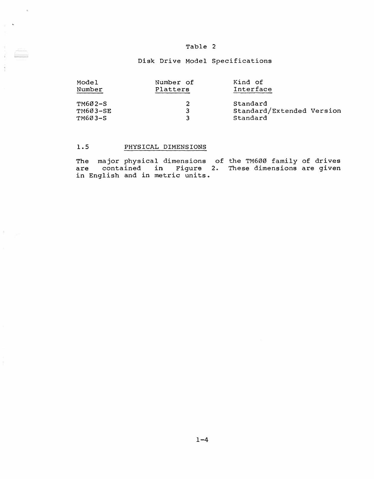
Tandon TM602S Service manual

TANDON
OEM
OPERATING
AND
SERVICE
MANUAL
MODEL
NUMBERS
TM602S, TM603S,AND TM603SE
5.25"
RIGID
DISK DRIVES
SEPTEMBER
20,
1982
PRELIM'
RY
TANDON
CORPORATION
20320
PRAIRIE
STREET
CHATSWORTH,
CA
91311
TEL.
NO.:
(
213)
993-6644
TWX
NO.:
910-494-1721
TELEX
NO.:
194794
TANDON
INTERNATIONAL
GMBH
AM
SUEDPARK
7A
D-6092
KELSTERBACB,
WEST
GERMANY
TEL.
NO.:
06
11/49
6107
2091
TELEX
NO.:
411547
pIN
187275-004
Rev
..
C

CONTENTS
Page
Number
SECTION
I--GENERAL
INFORMATION
1.1
Scope
1-1
1.2
Introduction
....•.•...............•.•.•
1-1
1.3
Disk
Drive
Performance
Characteristics.
1-1
1.4
Disk
Drive
Model
Specifications
.•••.•••
1-1
1.5
Pqysical
Dimensions
••..•...•.••.•.•..••
1-4
SECTION
II--INSPECTION,
INSTALLATION,
AND
INTERFACES
2.1
Introduction
••••••••••.••..•.••.•.•..••
2-1
2.2
Unpacking
and
Inspection
•••••••••••.•.•
2-1
2.3
Mounting
Characteristics
•••••••••••••.•
2-3
2.4
Power
Cabling
•••••••••••.••.•••••••••••
2-3
2.5
Standard
Interface
••••••••••.•.••••••••
2-3
SECTION
III--THEORY
OF
OPERATION
3.1
3.2
3.2.1
3.2.2
3.2.3
3.2.4
3.2.5
3.2
..
6
3.3
3.3.1
3.3.2
3.3.3
3.3.4
3.3.5
3.3.6
3.4
3.4.1
3.4.2
Introduction
.•..•.•••.••.•••••.••••.•••
3-1
Input
Control
Lines
••.•••••..••••••••••
3-2
Reduced
Write
Current
.•••.•••..••••.••.
3-2
Write
Gate
••••••.•••••••.•••••••••.••••
3-2
Head
Select
••••••••••.•••.•••••••••••••
3-3
Step
Interface
•••••••••••••••••••••••••
3-3
Di
rect
i
on
In
•••••••••••••••••.•••••••••
3-4
Drive
Select
••••••••••••.•••.••••••••••
3-4
Output
Control
Lines
••••.•••••••••••••••
3-5
Drive
Selected
•••••••••••••••••••••••••
3-5
Seek
Complete
••••••••••••••••••••••••••
3-5
Track
00eJ
••••••••••••••••••••••••••••••
3-5
Fault
0
••••••••••••
,.
••••
3-6
Line
Ready
•••••••••••••••••••••••••.•••
3-6
Index
3-6
Data
Transfer
Lines
••••••••••••••.•••••
3-6
MFM
Write
Data
•••••••••.••••••.••••.•••
3-6
MFM
Read
Data
••••••••••••••••••••••••••
3-7

Figure
Number
1
2
3
4
5
6
7
8
9
LIST
OF
ILLUSTRATIONS
FIGURES
Page
Title
Number
Typical
starting
Current
at
Nominal
Voltage
1-3
Disk
Drive
Physical
Dimensions
1-5
Locations
of
Interface
Connectors
2-2
J 3
Connector
........•.............•...••
2-
3
Jl
Connector
Dimensions
2-4
J2
Connector
Dimensions
••............•.•
2-4
Control
Signal
Driver/Receiver
Circuit
Combination
.•........••...•.•..•
3-1
Step
Mode
Timing
Diagram
•..•••...•.••..•
3-4
Data
Line
Driver/Receiver
Circuit
....•••
3-7
TABLES
Table
Number
Title
Page
Number
1
2
3
4
Disk
Drive
Performance
Characteristics
••
1-2
Disk
Drive
Model
Specifications
....•...•
1-4
Standard
Interface
...••........••...•..•
2-7
Head
Select
.•............•.••..•
"
.....
".
3-3
APPENDIX
Appendix
Number
Title
Page
Number
A
B
C~stomer
Information
Bulletins
•.......••
A-I
Schematics
""."
•..
"
..
"......................
B-1
ii

1.1
SECTION
I--GENERAL
INFORMATION
SCOPE
This
manual
contains
information
useful
in
the
installation
and
operation
of
Tandon
Corporation's
TM600
family
of
5.25"
rigid
disk
drives.
This
manual
also
contains
interface
requirements
and
descriptions
of
signals.
TM600
refers
to
Model
Numbers
TM602S,
TM603S,
and
TM603SE,
as
appropriate.
1.2
INTRODUCTION
The
TM600
family
of
5.25"
rigid
disk
drives
are
low-dost,
random
access
memories
that
use
moving
head,
noncontact
recording
techniques.
There
are
both
two-
and
three-platter
models,
which
use
standard
Winchester
technology
and
130
millimeter
rigid
media.
This
drive
consists
of
storage
media
that
is
contained
within
the
drive
in
a
fixed
(nonoperator
removable)
configuration,
read/write
and
control
electronics,
the
drive
mechanism,
a
read/write
head,
a
precision
split
band
positioning
device,
and
an
air
filtration
system.
Interface
flexibility
is
provided
by
using
an
industry
standard
interface
on
the
drive.
The
"s"
version
is
compatible
with
larger
capacity
disk
drives.
Compatible
is
defined
as
using
the
same
pin
assignment
where
the
signal
and
the
function
are
common.
1.3
DISK
DRIVE
PERFORMANCE
CHARACTERISTICS
The
information
contained
in
Table
1
pertains
to
all
Imodels
of
the
Tandon
TM600
family
of
disk
drives.
1.4
Table
2
and
the
DISK
DRIVE
MODEL
SPECIFICATIONS
contains
a
list
of
the
drive
models
number
of
platters
each
one
has.
1-1
available

Table
1
Disk
Drive
Performance
Characteristics
Model
TM602S TM603S TM603SE
Disks/Platters
Heads/Recording
Surfaces
2
4
3
6
3
6
TPI
II
Cit
•
II
••
II
••••
Cit
Cit
II
It
•••
41)
••
254
TPI
II
•••
0
..
II
.,
••
0 •
,.
•••••
II
••
Cylinders
153
153
230
RPfv1
•••••.••
Cit
•••••••
II
....
II
•••
e.
0 • 0
...
.,
•
Cit
,,3600
RPM +1
percent
...
0
••••
Cit
••••
Recording
Capacity,
Unformatted:
Per
Drive
6.38
MBytes
9.57
MBytes
14.35
MBytes
Per
Surface
1.59
MBytes
1.59
MBytes
2.39
MBytes
Per
Track
..•..•..•..•...••..
10
.40
KBytes
...•.....••....•.......••.
\I
Trans
fer
Rate
...•••.••..•.•••.•.••••...
5Mbi
ts
per
second
.•..•..•.•.••
Recording
Density
(BPI)
Tracks
7690
612
7690
918
9625
1380
milliseconds
.....•.••.•..•..••.•.••
••••••••••
0
•••••
3
153
ms,
99
ms
153
ms,
99
ms
210
ms,
137
rns
ramped
seek
ramped
seek
ramped
seek
Head
Settling
Time
••.....•..•.......
15
milliseconds
..........••..•.•
Average
Latency
..........•.•...•••
8.34
milliseconds
......••.........
7\ccess
Time
Track-to-Track
Average
Mechanical
Dimensions
Height
..
0
•••
0 0
.,
e
....
••••
., •
Cit
••
0 0
.,
••
3.
25
inch
I)
•••
.,
0
I)
It
......
II
......
0
II
..
6)
0
••
0
wid
th
0
Cit
,.
0 " 8' •
crt
••••
"5
I)
75
inch
CD
••••
It
4)
••
0
Cit
•(II
••
<>
0
CD
•
.,
• 0 0 0 •
Length.
fit
•••
Cit
..
"0
••••
,.
•
.,
••••
(III
co
..
(I
Cit
.8
11)
00
inch.,
..
0 0
••••••••
CD
" •
••
0 0
••
Cit
Cit
••
It
Error
Rates
Soft
Read
...•••••.•.••..•.•.•••...
lXl0
l0
bits
...•..••..••..••••••.••
Hard
Read
•.....•..••••••..•••.•••.
lX10
~
2
bits
..
Seek
Errors
.••.....•...•...•...•.•
1X10
seeks
...•••.•..••.•.•.•.•••.
Power
+l:2V
D.
C.
+/-
+5V
D.
C.
+/-
10%
1.5
amps
tyical,
5
amps
maximum
for
10
seconds
with
no
more
than
5
millivolts
PARD*
(see
Figure
I).
5%
..
8
amps
typical
with
no
more
than
50
millivolts
PARD*
Environmental
Ambient
Temperature:
Operating:
16°C
to
46°C
(50
0p
to
l15
0
p)
Nonoperating:
-35.4
0C
to
60°C
(~400p
to
140
0
P)
Relative
Humidity:
8%
to
80%
Maximum
Wet
Bulb
Temperature:
*Periodic
and
Random
Deviation.
Specifications
SUbject
To
Change
Without
Notice.
1-2

>
N
+>
I()
+
o
N
...
...
....
0
...
0)
[)
co
W
~
z
9
,.....
z
a::
::>
....
co
a::
w
....
u..
«
It)
w
~
i=
'I:f
o
Figure
1
Typical
Starting
Currents
At
Nominal
Voltage
1-3

Table
2
Disk
Drive
Model
Specifications
Model
Number
TM602-S
Tt1603-SE
TM603-S
1.5
Number
of
Platters
2
3
3
PHYSICAL DIMENSIONS
Kind
of
Interface
Standard
Standard/Extended
Version
Standard
The
major
physical
dimensions
of
the
TM600
family
of
drives
are
contained
in
Figure
2.
These
dimensions
are
given
in
English
and
in
metric
units.
1-4

0.06
±0.01 in.
(1.6 ±
0.3
mm)
TAPPED
MOUNTING
HOLES
FOUR
ON
BonOM.
TWO
ON
EACH SIDE
6·32
UNC
X
31
in
..
17.9
mml
DEEP
8
PLACES.
I
3.25
±0.01 in.
(82.6 ±
0.3
mm)
SIDE VIEW
3.12
±
0.02
in.
(79.2 ±
0.5
mm)
LJ
L87±OO2in
(47.5 ±0.5
mml
8.00
in.
maximum
--------
.......
1I
...--.--------
(203.2
mm)
I
0.19
±0.01 in.
(4.8 ±
0.3
mm)
3.38
±0.01 in.
85.9
±
0.3
mm)
5.88
±0.01 in.
(149.4
±
0.3
mm) BOTTOM VIEW
5.75
±
.02
in.
(146.1 ±
0.3
mm)
5.50
±
.02
in.
139.7±0.5
mm)
0.06
±0.01 in.
(1.6 ±
0.3
mm)
Figure
2
Disk
Drive
Physical
Dimensions
1-5

2.1
SECTION
II--INSPECTION,
INSTALLATION,
AND
INTERFACES
INTRODUCTION,
This
section
contains
information
pertinent
to
the
inspec-
tion,
installation,
and
interfaces
of
the
Tandon
TM600
family
of
rigid
disk
drives.
The
electrical
interface
between
the
drive
and
the
host
system
is
via
four
connectors.
Jl
provides
control
signals
for
the
drive.
J2
provides
for
the
radial
connection
of
read/write
data
signals.
J3
provides
for
D. C.
power.
J4
provides
for
frame
ground.
Figure
3
contains
the
locations
of
the
interface
connectors.
2.2
UNPACKING
AND
INSPECTION
The
drive
is
shipped
in
a
protective
container
which,
when
bulk
packaged,
minimizes
the
possibility
of
damage
during
shipment.
The
following
procedure
is
the
recommended
method
of
uncrating
the
drive.
1.
Place
the
shipping
container
on
a
flat
work
surface.
2.
Remove
the
upper
half
of
the
inner
container.
3.
Remove
the
drive
from
the
lower
half
of
the
inner
container.
4.
Check
the
model
number
and
top
assembly
description
against
the
packing
slip.
5.
Visually
examine
the
contents
of
the
shipping
container
for
possible
damage.
6.
Notify
the
is
found.
carrier
immediately
if
any
damage
7.
The
inside
chamber
of
the
drive
is
a
sealed
compartment
that
must
not
be
opened.
NOTE
REMOVAL
OF
THE
COVER
INVALIDATES
THE
WARRANTY.
2-1
OF
THE
DRIVE

FRONT
PANEL~
OR
CABLE
HOL~SS~4
PLACES)
HARNESS
V-AXIS
COMPONENT
SIDE
OF CIRCUIT BOARD
X-AXIS
Figure
3
Connectors
of
Interface
Locations
2-2

Before
applying
power
to
the
disk
drive,
inspection
procedure
should
be
performed:
the
following
1.
Check
to
ensure
that
the
circuit
boards
are
secure.
2.
Check
to
ensure
that
the
connectors
are
firmly
seated.
3.
Notify
the
carrier
immediately
if
you
find
any
damage.
2.3
MOUNTING
CHARACTERISTICS
The
mounting
characteristics
of
the
TM600
family
of
disk
drives
are
contained
in
Figure
2.
There
are
four
6-32,
tapped
mounting
holes
on
the
bottom
of
the
disk
drive,
and
two
on
each
side
of
it.
2.4
POWER
CABLING
The
D.C.
power
connector,
J3,
is
a
four-pin
AMP
Mate-N-Lok
device,
pIN
350211-1,
which
is
mounted
on
the
solder
side
of
the
circuit
board.
The
recommended
mating
connector,
P3,
is
AMP
piN
1-480424-0,
using
AMP
pins
pIN
60617-4.
J3
pins
are
labeled
on
the
J3
connector.
Figure
4
contains
an
illustration
of
the
J3
connector.
Figure
4
J3
Connector
The
frame
ground
connector,
J4
is
the
Faston
AMP
pIN
61761-2.
The
recommended
mating
connector
is
AMP
pIN
62187-1.
2.5
STANDARD
INTERFACE
The
standard
or
usu
model
interface
is
contained
in
Table
2-1.
Connection
to
Jl
is
via
a
34-pin
circuit
board
edge
connector.
~The
dimensions
of
the
Jl
connector
are
found
in
Figure
5.
The
pins
are
numbered
1
through
34.
The
even
numbered
pins
are
located
on
the
compoenent
side
of
the
circuit
board.
Pin
2
located
on
the
end
of
the
circuit
board
connentor
closest
to
the
D.
C.
power
connector
J3/p3,
and
it
is
labeled.
A
key
slot
is
located
between
Pins
4
and
6.
2-3

0.063
in.
(1.6 mm)
l[
lr
0.036
±
0.004
In.
(0.91 ±
0.'
mml
2 4
--11-
0050
in.
(1.27
mm)
--..!.l
WO.050
in.
(1.27
mm)
~
J4I
0.100
in.
(2.54
mm)
~-------_
1.775
±
0.010
in.
-...
..
1
(45.1 ±
0.25
mm)
,r
.....
,...
.....
r---J
)
.....
--
oin.
0.450
in.
(11.4
mm)
----i'"'
--
mm)
I,
~
I,
I
J
t
0.400
±0.01
(10.2
±
0.25
BOARD
THICKNESS
0.062
±
0.007
in.
(1.59
mm
±
0.18
mm)
Figure
5
Jl
Connector
Dimensions
,...-
0.063
in.
, _ (1.6 mm)
BOARD
THICKNESS
0.062
±
0.007
in.
(1.59
mm
±
0.18
mm)
0.050
in.
(1.27
mm)
0.100
in.
(2.54
mm)
0.050
in. II I
-lll~~
,_
(1.27
mm)
--;-'iLr-
---l
I.
I
.
1.075±0.010in.~
(27.3
±
0.25
mm)
0.036
±O.•
004
in'1r--
(0.91 ±0.1
mm)
I
---~5
2
--.......-
1
0.400
±
0.010
in.
10.2
±
0.25
mm)
_t
Figure
6
J2
Connector
Dimensions
2-4

The
recommended
mating
connector
for
PI
is
a
3M
ribbon
connector,
pIN
3463-0001,
without
ears.
connection
to
J2
is
via
a
20-pin
circuit
board
edge
con-
nector.
The
dimensions
of
the
J2
connector
are
found
in
Figure
6.
The
pins
are
numbered
1
through
20.
The
even
numbered
pins
are
located
on
the
component
side
of
the
circuit
board.
The
recommended
mating
connector
for
P2
is
a
3M
ribbon
connector,
pIN
3461-0001,
without
ears.
A
key
slot
is
located
between
Pins
4
and
6.
2-5

Table
3
Standard
Interface
Connector
Interface
Pin
Number
Signal
(Gnd)
Signal
Type
I/O
Signal
Name
PI
A
34-Pin
Ribbon
Daisy
Chain
P;
I
20-Pin
Ribbon
Daisy
Chain
or
R?dial
~
P2
P~
4-pin
Power
Radial
p~
2
4
6
8
10
12
14
16
18
20
22
24
26
28
30
32
34
1
3
5
7
9
11
13
14
15
17
18
19
1
2
3
4
(
1)
(
3)
( 5 )
(
7)
(9
)
(11)
(13)
(15)
(17)
(19
)
(21)
(
23)
(25)
(27)
(29)
(31
)
(33)
(
2)
(4
)
(6)
(8)
(10
)
(12)
(16)
(20
)
S
S
S
S
S
S
S
S
S
S
S
S
S
S
S
S
S
S
S
D
D
D
D
I
I
o
o
o
I
I
o
o
I
I
I
I
I
I
o
I
I
I
o
o
Reduce
Write
~
Head
Select
2
Write
Gate
Seek
Complete
Track
000
Fault
Head
Select
20
Reserved
(To
i2-7)
Head
Select
2
Index
Ready
Step
Drive
Select
0
Drive
Select
1
Drive
Select
2
Drive
Select
3
Direction
In
Drive
Selected
Reserved
(+5
V)
Reset
Reserved
(TO
Jl-16)
Spare
Ground
+
Write
Data
-
Write
Data
Ground
+
Read
Data
-
Read
Data
Ground
+12
VD.
C.
In
12
V
Return
5 V
Return
+5 VD. C.
In
Notes:
1.
S -
Single
ended
2.
D -
Differential
2-6
3.
I -
Drive
input
4.
0 -
Drive
output

3.1
SECTION
III--THEORY
OF
OPERATION
INTRODUCTION
There
are
three
kinds
of
interface
signals:
1.
Input
Control
Lines
2.
Output
Control
Lines
3.
Data
Transfer
Lines
Signals
on
the
Input
Control
lines
are
standard
TTL
levels.
They
have
the
following
electrical
specifications:
True:
0.0
volt
D.
C.
to
0.4
volt
D.
C.
@I=
40
rnA
maximum
False:
2.5
volt
D.
C.
to
5.25
volt
D.
C.
@I=0
rnA
open
See
Figure
7
for
the
recommended
circuit.
+
5V
7438
OR
EaUiVAlENT
20
FT.
MAXIMUM-'
Figure
7
220Q
74LS14
OR
EaUIVALENT
Control
Signal
Driver/Receiver
Circuit
Combination
3-1

3.2
INPUT
CONTROL
LINES
There
are
two
kinds
of
Input
Control
lines,
those
that
are
multiplexed
in
a
multiple
drive
system
and
those
that
do
the
multiplexing.
The
Input
Control
lines
that
are
mUltiplexed
include:
1.
Reduced
Write
Current
2.
Write
Gate
3.
Head
Select
4.
Step
Interface
5.
Direction
In
The
Input
Control
lines
that
do
the
multiplexing
are:
1.
Drive
Select
0
2.
Drive
Select
1
3.
Drive
Select
2
4.
Drive
Select
3
3.2.1
Reduced
write
Current
When
this
Input
Control
line
is
activated
low'(true)
in
conjunction
with
the
write
gate,
a
lower
value
of
write
current
is
selected
for
writing
on
the
disk.
When
the
signal
is
set
high
(false),
the
higher
value
write
current
is
selected.
When
writing
on
Tracks
0
through
127,
it
is
recommended
that
this
line
be
set
false.
For
Tracks
128
and
greater,
the
Reduced
Write
Current
line
should
be
set
true.
A
220/230
ohm
resistor
pack
allows
the
line
to
be
terminated.
3.2.2
Write
Gate
The
Write
Gate
signal
enables
data
to
be
written
on
the
disk
when
it
is
activated
or
when
the
logical
zero
(true)
level
is
reached.
The
ready
line
must
be
valid
before
write
gate
is
activated.
If
a
disk
drive
fault
occurs,
further
writing
on
the
disk
is
propibited.
In
addition,
the
Seek
Complete
line
should
go
true
before
you
begin
to
write
any
information
on
the
disk.
The
line
inactive
or
logical
high
(false)
level
on
the
Write
Gate
enables
the
step
pulses
to
step
the
head,
arm
actuator.
3-2

3.2
..
3
Head
Select
There
are
three
Head
Select
lines.
They
are
used
to
select
each
read/write
head--0,
1,
or
2--in
a
binary
coded
sequence.
Head
Select
signals
are
logic
low
(true)
levels.
They
must
be
activated
in
conjunction
with
the
Drive
Select
lines.
The
heads
are
numbered
0
through
5.
Head
Select
0
is
the
least
significant
line.
Table
3-1
contains
information
about
the
Head
Select
line
sequence,
disk
drive
model
number,
and
numbers
that
may
be
selected.
Table
3-1
Head
Select
Head
Select
Line
Sequence
Model
Number
22
2120TM602 TM603
Head
Number
Selected
11 1 00
11011
10 1 2 2
1
(2}
033
01 1 4
(2}
1
(2}
5
Legend:
1=
Logical
High
(False)
(2}
=
Logical
Low
(True)
A
220/330
ohm
resistor
pack
allows
the
line
to
be
terminated.
3.2.4
Step
Interface
When
the
Step
Interface
line
is
activated
in
conjunction
with
the
Direction
In
line,
the
read/write
heads
move
in
the
direction
defined
by'
the
Direction
In
line.
The
motion
is
initiated
by
a
logical
zero
to
a
logical
one
transition
or
by
the
trailing
edge
of
the
step
pulse.
Any
change
in
the
Direction
In
line
must
be
made
one
hundred
nanoseconds
before
the
leading
edge
of
the
step
pulse.
The
quiescent
state
of
this
line
should.
be
held
logically
high
(false).
The
heads
move
at
the
rate
of
the
incoming
step
pulses.
Figure
8
contains
the
sequence
and
the
requirements
for
step
timing.
3-3

,
00
NS
MINIMUM.
200
US
MAXIMUM
500
NS
MAXIMUM
-STEP
--I
!~
f/?2Z7],---~1
If
I
~
3.0
MS
MINIMUM
--IIj
~1
loOllllllll--'·O
US
MINIMUM
!.-
STEP LOGIC
Ur----I)
f
ENERGIZED I
I
4111(15
+3
MS~
4-
ITYPICAL
...----------------1,
-SEEK
COMPLETE
---------',
'----
DIRECTION IN
Figure
8
step
Mode
Timing
Diagram
3.2.5
Direction
In
The
Direction
In
line
determines
the
motion
of
the
read/write
heads
when
a
step
pulse
is
issued.
The
motion
is
toward
the
center
of
the
disk
if
the
Direction
In
line
is
in
the
true
(low)
state
when
a
step
pulse
occurs.
The
direction
of
the
motion
is
away
from
the
center
of
the
disk
if
the
Direction
In
line
is
in
the
false
(high)
state
when
a
step
pulse
occurs.
A
220/330
ohm
resistor
pack
allows
the
line
to
be
terminated.
3.2,,6
Drive
Select
Drive
Select
lines
0
through
3
provide
a
means
of
selecting
and
deselecting
a
drive.
These
four
lines
select
one
of
four
drives
that
are
daisy
chained
to
the
controller.
The
drive
address
is
determined
by
a
select
shunt
on
the
Signal
circuit
board.
Drive
Select
lines
0
through
3
provide
a
means
of
daisy
changing
amaximum
of
four
drives
to
a
controller.
When
logically
high
(false),
the
output
drivers
are
open
circuits
or
logically
high
(false),
and
the
drive
receivers
do
not
acknowledge
signals
presented
to
them.
A
Drive
Select
line
must
remain
stable
in
the
true
(low)
state
until
a
Step
or
Read/Write
command
is
executed.
Only
one
line
can
be
true
(low)
at
a
time.
An
undefined
operation
might
result
if
two
or
more
units
are
assigned
the
same
address
or
if
two
or
more
Drive
Select
lines
are
in
the
true
(low)
state
simultaneously.
3-4

3.3
OUTPUT
CONTROL
LINES
The
Output
Control
lines
are
enabled
by
their
respective
Drive
Select
line.
They
send
status
information
to
the
controller,
such
as:
drive
selected,
seek
complete,
Track000
fault,
and
line
ready.
In
addition,
the
Index
line
is
pro-
vided
as
an
output
to
the
controller
for
timing
information.
The
Output
Control
lines
use
an
open
collector
gate
that
is
capable
of
sinking
a
maximum
of
forty
milliamperes
in
a
logical
low
(true)
level,
with
amaximum
voltage
of
0.4
volt
measured
at
the
driver.
When
the
gate
is
off
or
logically
high
(false),
the
collector
cutoff
is
amaximum
of
250
u
am~s.
See
Figure
8
for
the
recommended
circuit.
3.3.1
Drive
Selected
When
the
Drive
Selected
lines
coincide
with
the
selected
jumper
on
the
shunt
pack,
the
Select
Status
line
goes
logically
low
(true).
This
line
informs
the
host
system
of
the
selection
status
of
the
drive.
NOTE
ONLY
ONE
DRIVE
MAY
BE
SELECTED
AT
A
TIME.
3.3.2
Seek
Complete
~he
Seek
Complete
line
indicates
that
the
read/write
heads
have
settled
on
the
selected
track
at
the
end
of
a
seek
sequence.
This
status
line
is
set
logically
zero
(true)
at
the
end
of
a
normal
seek.
It
is
set
logically
high
(false)
in
two
cases:
1.
A
recalibration
sequence
is
initiated
by
drive
logic
at
power
on
because
the
heads
are
not
over
Track
000.
2.
Five
hundred
nanoseconds,
typical,
after
the
leading
edge
of
a
step
pulse
or
of
a
series
of
step
pulses.
3.3.3
Track
000
The
Track
read/write
line
goes
tioned
on
moved
away
000
line
indicates
to
the
host
system
that
the
heads
are
positioned
on
Track
000.
The
Track
000
logically
low
(true)
only
When
the
heads
are
posi-
Track
000.
It
remains
low
until
the
heads
are
from
Track
000,
the
outermost
data
track.
3-5

3.3.4
Fault
The
Fault
line
indicates
to
the
host
system
that
a
condition
exists
on
the
disk
drive
that
is
going
to
cause
improper
writing
on
the
disk.
When
this
line
is
logically
low
(true),
Write
Data
is
inhibited
and
further
writing
on
the
disk
is
pro-hibited
until
the
condition
is
corrected.
The
condition
under
which
the
Fault
line
goes
true
is
that
D.C.
voltages
are
grossly
out
of
tolerance.
3.3.5
Line
Ready
In
conjunction
with
the
Seek
Complete
line,
the
Line
Ready
line
indicates
to
the
host
system
that
the
disk
drive
can
read,
write
or
seek,
and
that
all
I/O
signals
are
valid.
The
Line
Ready
line
goes
logically
low
(true)
approximately
15
seconds
after
power
on.
The
Line
Ready
line
goes
logically
high
(false)
if
the
drive
is
not
selected
or
if
the
speed
of
the
motor
is
too
slow.
When
this
line
is
false,
all
writing
and
seeking
is
inhibited.
3.3
..
6
Index
An
index
pulse
is
provided
once
every
revolution
(16.67
ms
nominal)
to
indicate
the
beginning
of
a
track
to
the
con-
troller.
The
transition
from
logically
high
(false)
to
logically
low
(true)
is
the
only
valid
transition.
The
leading
edge
of
the
pulse
must
be
used
to
ensure
accurate
timing.
3.4
DATA
TRANSFER
LINES
The
Data
Transfer
lines
transfer
information
between
the
host
system
and
the
disk
drive
when
the
drive
is
selected.
These
lines
are
differential
in
nature.
They
may
be
multiplexed
when
us
ing
Drive
Se
lect
.0
The
MFM
Write
Data
pair
of
lines
and
the
MPM
Read
Data
pair
of
lines
are
provided
for
the
transfer
of
data.
Figure
9
contains
q
typical
driver/receiver
circuit
combination
used
for
data
transfer
signals.
3.4.1
The
MFM
provide
on
the
MFM
Write
Data
Write
Data
lines
are
the
differential
pair
that
the
data
to
be
stored
on
the
track.
A
flux
reversal
track
to
be
written
is
caused
When
the
plus
(+)
MFM
3-6
This manual suits for next models
2
Table of contents
Other Tandon Storage manuals
Popular Storage manuals by other brands

Exabyte
Exabyte X200 Library Installation and operation

Qualstar
Qualstar RLS-8350 Product specification

MXI Security
MXI Security stealth hd bio quick start guide

NETGEAR
NETGEAR SC101 - Storage Central NAS Server Installation overview

Edge10
Edge10 EDGESTORE NAS400 user manual

Dell
Dell PowerVault DL4000 owner's manual