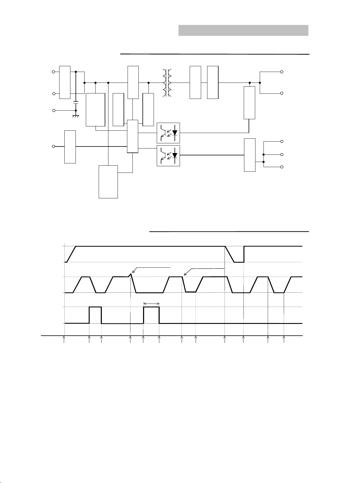
PAH300・350S24-SERIES
TDK-Lambda
8
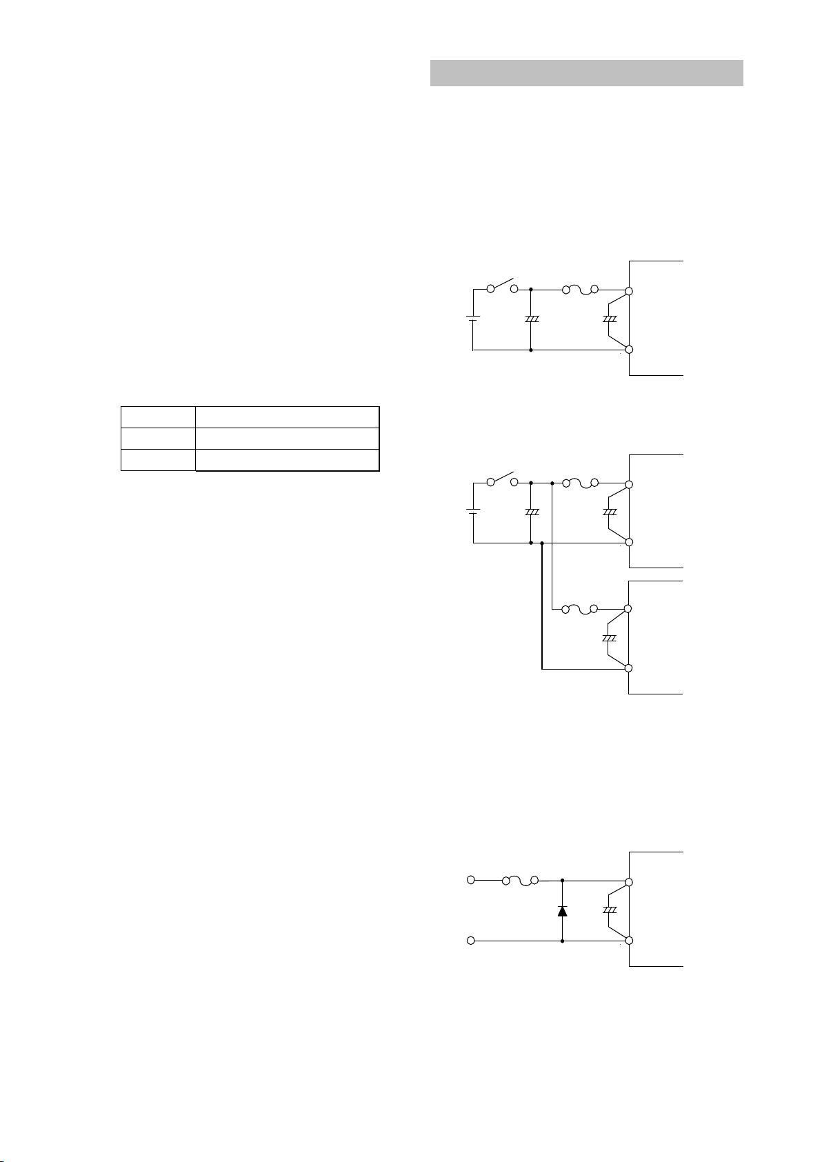
3. Maximum Ripple and Noise
Measured value according to the specified methods
based on JEITA-9141 (Clause 7.12 and clause 7.13)
which is described in the following.
Connect according to fig.3-1 and measure. Connect
capacitors (C2, C3: film capacitor or ceramic capacitor
0.022μF) between output terminals and the nearest
M3 threaded hole. Connect capacitors (C4: refer to
table 1-1 for electrolytic capacitor values, C5: ceramic
capacitor 0.1μF) at 50mm distance from the output
terminals. Measure at ceramic capacitor (C5) terminals
as shown in fig. 3-1 using coaxial cable with JEITA
attachment. Use oscilloscope with 100MHz frequency
bandwidth or equivalent.
Take note that output ripple voltage and output spike
noise may vary depending on PCB wiring design.
Generally, output ripple voltage and output spike
noise can be reduced by increasing capacitance value
of external capacitor.
JEITA Attachment
R:50Ω
C:4700pF
+
50mm
+V
-V
As short as possible
Coaxial Cable
1.5m 50Ω
C5
C4
R
C
C2
C3
Load
-S
+S
Fig.3-1 Measurement of Maximum Output Ripple &
Noise
4. Maximum Line Regulation
Maximum value of output voltage change when input
voltage is gradually varied (steady state) within
specified input voltage range.
5. Maximum Load Regulation
Maximum value of output voltage change when
output current is gradually varied (steady state) within
specified output current range.
When using at dynamic load mode, audible noise
could be heard from the power module and output
voltage fluctuation might increase. A thorough pre-
evaluation must be performed before using this power
module.
6. Over Current Protection (OCP)
This power module has built-in OCP function.
Output will recover when short circuit or overload
conditions are released. OCP setting value is fixed and
therefore, cannot be externally adjusted.
Also, take note that power module might be damaged
continuing output short circuit or over load conditions
depending on thermal conditions.
7. Over Voltage Protection (OVP)
This power module has built-in OVP function.
OVP set point is relative to the rated output voltage
value. OVP setting value is fixed and therefore, can not
be externally adjusted.
When OVP is triggered, output can be recovered by
turning input line off and then turning it on again after
lowering the input voltage below the voltage value
indicated below, or by manual reset of the CNT
terminal. Reset time for CNT terminal is 100ms or
longer.
OVP release input voltage value : 3VDC and below
When verifying OVP function by applying external
voltage at the output terminals, applied voltage value
should not exceed specified OVP maximum value.
Refer to specification table for OVP maximum value.
Avoid applying external voltage that exceeds OVP
maximum value because this will cause power module
damage.
8. Over Temperature Protection (OTP)
This power module has built-in OTP function.
This function operates and shuts down the output when
ambient temperature or internal temperature of power
module abnormally rises. OTP operates at 105℃ to
130℃ baseplate temperature. OTP can be released when
baseplate temperature drops down approximately to
within 80℃ to 95℃. However, take note that OTP will
operate again unless the cause of abnormal heat of the
power module is eliminated.
9. Remote Sensing (+S, -S terminal)
Remote sensing terminal is provided to compensate for
voltage drop across the wirings from the power module
output terminal to the load input terminal.
When remote sensing function is not used (local sensing),
short +S terminal to +V terminal and, –S terminal to –V
terminal.
Take note that voltage compensation range for line
drop (voltage drop due to wiring) is determined such
that output voltage at the output terminals is within
output voltage range and that voltage between –V and –
S terminals is within 2V or less. Even for remote
sensing case, use power module such that output power