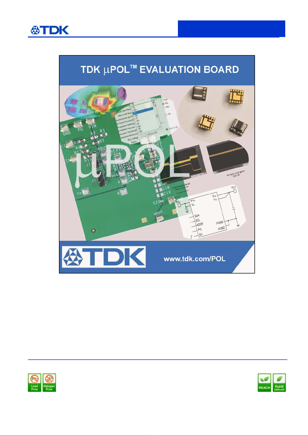
Page 3
Rev 1.0, Jun 1, 2022
Patent Protected: US 9,729,059 B1; US 10,193,442 B2
Copyright© 201 –20 TDK Corporation. All rights reserved.
All registered trademarks and trademarks are the property of their respective owners.
Data and specifications subject to change without notice.
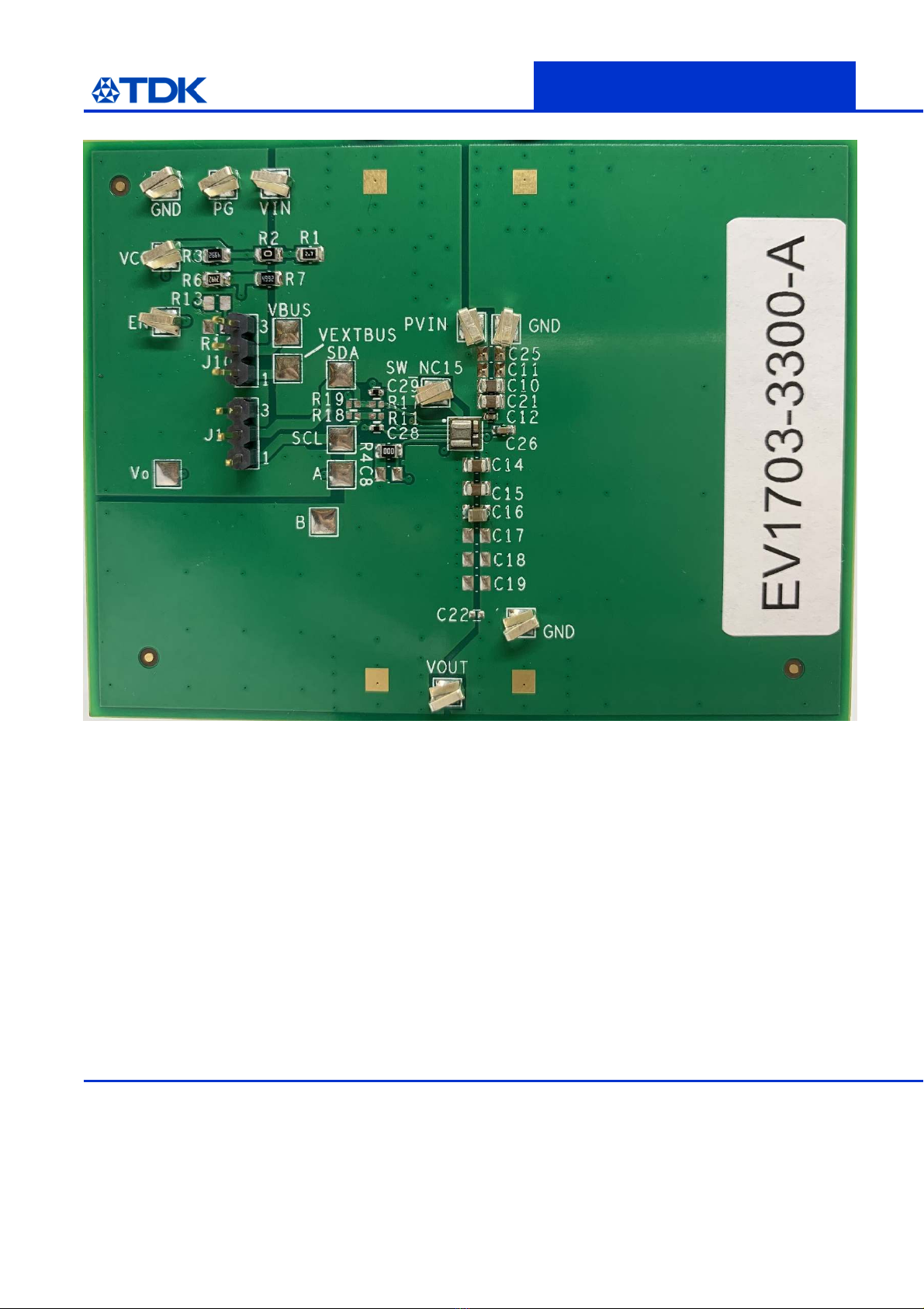
Descrip ion
The evaluation board consists of a 4-layer PCB made from FR4 glass-reinforced epoxy laminate material. All layers use
2oz copper (equating to a thickness of 0.0694mm). The major power components, including the FS1703, are mounted
on the top side of the board.
Par reference Quan i y Type Descrip ion
FS1703 µPOL 1 – Main IC
C10, C21 2 22µF 0 05, 16V, X5R
C12 1 0.1µF 0402, 16V, X7R
C13 1 6 µF 25V
C14, C15, C16 3 22µF 0 05, 6.3V, X5R
C26 1 1µF 0603, 25V, X5R
J1 1 Red Banana connector
J2, J7 2 Black Banana connector
J 1 Green Banana connector
J10, J11 2 – 3-pin header
R1 1 2.7Ω 10%, 1/ W, 0 05 case size
R3, R7 2 49.9kΩ 10%, 1/ W, 0 05 case size
R2, R4, R9 3 0Ω 0 05 case size
C2 , C29 2 0Ω (Note 1) 0402 case size
R6 1 24.9kΩ 10%, 1/ W, 0 05 case size
VIN, PG, EN, VCC, SW_NC15, VOUT, PVIN, GNDs 10 – Test points
Note 1: 0ohm is placed on capacitor footprint to ground NC pin.
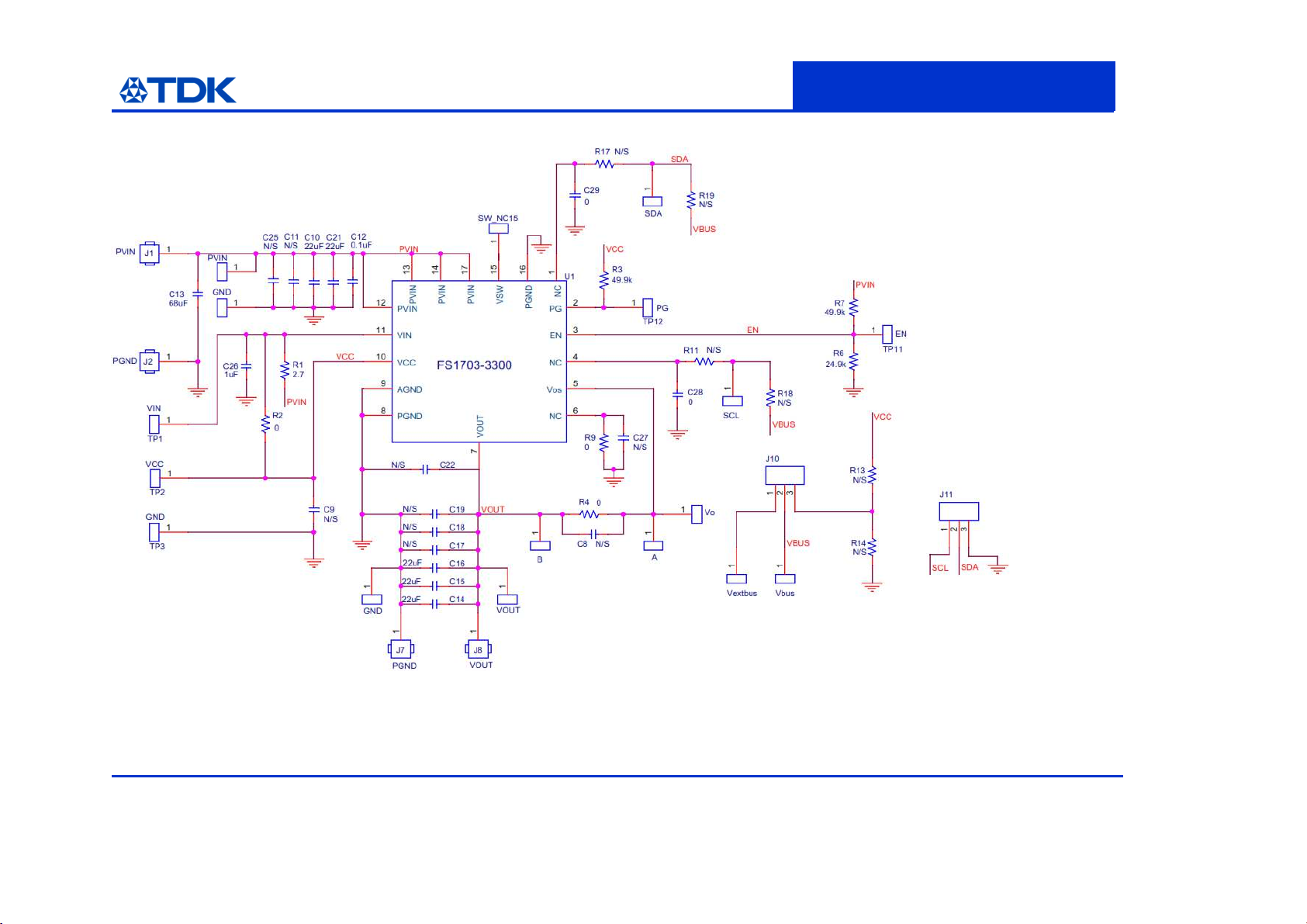
Figure 1 shows the layout of the board and Figure 2 shows a schematic of the electrical circuit.