manuals.online logo
Brands
  1. Home
  2. •
  3. Brands
  4. •
  5. Technics
  6. •
  7. CD Player
  8. •
  9. Technics SL-P250 User manual

Technics SL-P250 User manual

ORDER
NO.
HAD8803055C0
ervice
Manual
Compact
Disc
Player
SL-P250
(K)
ween
USA,
(K)
Canada.
(K)
(S)
Continental
Europe.
United
Kingdom.
COMPACT
[DIGITAL
|
DIGITAL
AUDIO
(K)
(S)
|
(EK)
(K)
(XL)
Australia.
(K)
(S)
|
(EG).......
F.R.
Germany.
(K)
(S)
Belgium.
(K)
(S)
Holland.
(K)
(S)
France.
(K)
(S)
|
(Ei)
Italy.
(K)
(XA)
Asia,
Latin
America,
Middle
Near
East,
Africa
and
Oceania.
Saudi
Arabia.
Far
East
PX.
European
Military.
Color
European
Audio
Club.
(K)...Black
Type
SPECIFICATIONS
i
Audio
i
Infrared
remote-control
transmitter
61x19
x
165mm
No.
of
channels
Frequency
response
Output
voltage
Dynamic
range
SIN
ratio
Harmonic
distortion
Total
harmonic
distortion
Wow
and
flutter
Output
impedance
Load
impedance
Headphone
output
level
D-A
conversion
system
@
Signal
Format
Sampling
frequency
D-A
conversion
@
Pickup
Wavelength
2
(left
and
right
stereo)
2~20,000Hz+0.5dB
2V
(at
OdB)
94dB
96dB
0.003%
(1kHz,
0dB)
0.006%
(1kHz,
0dB)
Below
measurable
limit
Approx.
600Q
More
than
10kQ
15mW
max.
32Q
(adjustable)
2
DAC
System
with
16-bit
Resolution
44.1kHz
16-bit
linear
780nm
Dimensions
(W
x
H
x
D)
:
(2-13/32”
x3/4”
x
6-1/2")
Batteries
UM-4
“AAA”
batteries
or
1EC
R03
or
equivaknt
(1.5V
x
2)
Weight
105g
(3.7
oz.)
(including
batteries)
i
General
Power
supply
For
U.S.A.
and
Canada.
:
AC12OV,
60Hz
For
United
Kingdom
and
Australia:
AC24OV,
50Hz
For
Continental
Europe:
AC22OV,
50Hz
For
Others:
AC
110V/127V/220
V/24V,
50/60Hz
Power
consumption
For
U.S.A.
and
Canada:
13W
For
)thers:
11W
Dimensions
(W
x
H
x
D)
430
x
7).8
><
247mm
(16-15/16"
x
3-5/37
x
9-23/32")
Weight
31kg
(6.8
Ib.)
Specifications
are
subject
to
change
without
notice.
Weight
and
dimensions
shown
are
approximae.
Matsushita
Electr:
Tras
ding
Co.,
Ltd.
Matsushita
Services
Company
Panasonic
Hawaii,
Inc.
50
Meadowland
Parkway,
91-238,
Kauhi
St.
Ewa
Beach
P.O.
Box
288,
Cerral
Csaka
Japan
Secaucus,
New
Jersey
07094
P.O.
Box
774
Honolulu,
Hawaii
96808-0774
Panasonic
Tokyo
iffice?
Matsushita
Elecir;
tras
ding
Co.,
Ltd.
Division
of
Matsushita
Electric
Matsushita
Electric
6th
Floor,
world
Tade
Center
Bidg.,
of
Puerto
Rico,
Inc.
of
Canada
Limited
No.
4-1,
HarmamMatu-ct»
o
2-Chome,
Ave.
65
De
Infanteria,
Km.9.7
5770
Ambler
Drive,
Mississauga,
Minato-ku,
Tokyo
05,
sapan
Victoria
Industrial
Park
Ontario,
L4W
2T3
Carolina,
Puerto
Rico
00630
Panasonic
Sales
Company,
Technics
SL-P250
Mi
CONTENTS
Page
Page
SAFETY
PRECAUTIONS
............0.2200ccucceccecucsees
2
PRINTED
CIRCUIT
BOARD
AND
PRECAUTION
OF
LASER
DIODE
...............0.ccceeee>
3
WIRING
CONNECTION
DIAGRAM
................:.
29
BEFORE
USING
THIS
UNIT
..............02-0ecneeeceeeee
3
PRINTED
CIRCUIT
BOARDS
.................0000005
30~34
CONNECTIONS
........2.-
ccc
cce
cece
cee
ceeceenecencauenes
4
BLOCK
DIAGRAM
...............ccccccceccuccercucs
35~37
CONCERNING
COMPACT
DISCS.
...................
aah
nie
ne
4
REMOTE-CONTROL
UNIT
PARTS
.............ccecceeees
38
FRONT
PANEL
CONTROLS
AND
FUNCTIONS.
..........
5,6
SCHEMATIC
DIAGRAM
OF
REMOTE-CONTROL
TRANSMITTER
............2.0.e0e008
7
REMOTE-CONTROL
TRANSMITTER
................-
39
HANDLING
PRECAUTIONS
FOR
OPTICAL
PICKUP
.......
8
INTERNAL
CONNECTION
OF
FL
..............20c0ccecee
40
INSTRUCTIONS
FOR THE
SZZOL31............2..cceeeaee
8
TERMINAL
GUIDE
OF
IC’S,
DISASSEMBLY
INSTRUCTIONS
................0.0005
9~12
TRANSISTORS
AND
DIODES
........
Sea
deena
40
MEASUREMENTS
AND
ADJUSTMENTS
.............
13~18
SCHEMATIC
DIAGRAM
...........0..cccccceccaccees
41~46
TERMINAL
FUNCTION
OF
LSI
...............2.00005
19~23
REPLACEMENT
PARTS
LIST
(Mechanical
parts)
.........
47
REPLACEMENT
PARTS
LIST
(Electrical
parts)........
24,
25
EXPLODED
VIEWS
.............ccccecccececcacccans
48~50
PACKING
0550
isceleectde-cas
ove-seh
et
adisacleca
dee
eeeee
cdmaees
26
TROUBLESHOOTING
GUIDE
.................000000e
51~54
RESISTORS
AND
CAPACITORS
.............00cce00s
27,
28
@
SAFETY
PRECAUTION
atis
“safety
precautions”
is
applied
only
in
U.S.A.)
Before
servicing,
unplug
the
power
cord
to
prevent
an
electric
shock.
When
replacing
parts,
use
only
manufacturer’s
recommended
components
for
safety.
.
Check
the
condition
of
the
power
cord.
Replace
if
wear
or
damage
is
evident.
.
After
servicing,
be
sure
to
restore
the
lead
dress,
insulation
barriers,
insulation
papers,
shields,
etc.
.
Before
returning
the
serviced
equipment
to
the
customer,
be
sure
to
make
the
following
insulation
resistance
test
to
prevent
the
customer
from
being
exposed
to
a
shock
hazard.
e
INSULATION
RESISTANCE
TEST
1.
Unplug
the
power
cord
and
short
the
two
prongs
of
the
plug
with
a
jumper
wire.
2.
Turn
on
the
power
switch.
3.
Measure
the
resistance
value
with
ohmmeter
between
the
jumpered
AC
plug
and
each
exposed
meta!
cabinet
part,
such
as
screwheads
antenna,
contro!
shafts,
handle
brackets,
etc.
Equipment
with
antenna
terminals
should
read
between
3MQ
and
5.2MQ
to
all
exposed
parts.
(Fig.
A)
Equipment
without
antenna
terminals
should
read
approximately
infinity
to
all
exposed
parts.
(Fig.
B)
Note:
Some
exposed
parts
may
be
isolated
from
the
chassis
by
design.
These
will
read
infinity.
OfRON
=
Antenna
terminal
Exposed Exposed
metal
metal
part
part
Ohmmeter
Ohmmeter
(Fig.
A)
(Fig.
B)
Resistance
=
3M2—5.2MQ
Resistance
=
Approx
oo
4.
lf
the
measurement
is
outside
the
specified
limits,
there
is
a
possibility
of
a
shock
hazard.
The
equiomnnt
should
be
repaired
and
rechecked
before
it
is
returned
to
the
customer.
*AC
power
supply
cord
....
1
Stereo
connection
cable...........
1
®Remote-control
eBatteies
-...-..
2
SJA175-1
(M)
(SJP2249-1)
transmitter
.....
1
pr
aera!
SJA172
(MC)
a
SJA187
(E,
EB,
EH,
EG,
EF,
Ei)
SJA173
(XL)
)
SFDACO5G02
(Ek)
SJA168
EUR64786
(M,
MC)
(XA,
PA, PE,
PC)
EUR64787
(others)......
Blaciverssion
SJA183
(XB)
EUR64792
(others)......
Silveverssion
Mi
PRECAUTION
OF
LASER
DIODE
Caution:
This
product
utilizes
a
laser
diode.
ADVARSEL:
|
dette
a
apparat
anvendes
laser.
®
Use
of
caution
labels
Note
©
Mark
is
used,
X
Mark
is
not
used
[EK],
[XL],
(EG),
(EB),
(EH),
(EF,
(Ei),
[XA},
[XB]
SQWD45
ADVARSEL
-Usynligt
laserlys
udstrales
ved
Abning
UNDGA
DIREKTE
BESTRALING.
SQw010
DANGER-
Invisible
laser
radiation
when
open.
AVOID
DIRECT
EX—
POSURE
TO
BEAM.
saw045
"CAUTION-nazaroous
Laser,
ano
ELECTROMAGNETIC
RADIATION
WHEN
OPEN”
"ATTENTION-ravonnement
Laser
Er
ELECTROMAGNETIOUE
DANGEREUX
SI
OUVERT”
SQWD19
Mi
BEFORE
USING
THIS
UNIT
The
optical
pickup
is
secured
to
prevent
damage
during
transport.
Be
sure
to
release
it
before
use.
(m)
(MB)
Lock
shaft
(in
the
locked
condition)
Pull
to
unlock.
Soft
cloth
or
similar
material
(to
prevent
scratches)
Caution:
Do
not
transport
the
unit
without
locking
the
lock
shaft.
Severe
damage
will
result.
If
the
unit
is
transported
again,
perform
the
following
steps:
1)
Remove
the
disc
from
the
tray
and
turn
off
the
power.
2)
Place
the
unit
with
the
rear
panel
facing
downward.
3)
Push
thelock
shaft
to
the
in
(LOCK)
position
(
Am
).
VAROITUS!
Laite
sisaltaa
laserdiodin,
joka
lahettaa
nakymatonta
silmille
vaarallista
lasersateilya
CLASS
1
LASER
PRODUCT
‘saw0?
Obs:
Apparaten
innehaller
laser
Komponent
av
hoger
laserklass
an
klass
1,
B®
Place
ona
flat,
level
surface
so
that
the
front-rear
inclination
does
not
exceed
5°.
@
Avoid
places
such
as
the
following:
Near
any
equipment
or
device
that
generates
strong
magnetism.
©
On
any
heat-generating
equipment
or
device,
or
in
any
place
where
the
temperature
is
high
(40°C
or
higher).
Extremely
cold
places
(5°C
or
below).
Near
a
tuner
or
TV
(It
may
cause
noise
in
the
broadcast,
or
disturbance
of
the
TV
picture.)
¢For
long
periods
of
time
in
direct
sunlight.
e|n
dusty
or
smoky
locations.
In
locations
prone
to
vibrations.
@{n
locations
where
the
rear
panel
is
less
than
10
cm
(about
4”)
away
from
the
wall
or
back
of
an
audio
rack.
eWithin
reach
of
children.
@
Donot
place
heavy
objects,
other
than
system
components,
on
top
of
the
unit.
@
When
carrying
or
storing
the
unit,
handle
it
with
care
so
it
is
not
subjected
to
any
strong
bumps.
Always
remove
the
disc
before
storing
the
unit
for
any
period
of
time.
—™
To
avoid
problems
due
to
vibration.
¢Do
not
place
a
book
or
similar
object
under
this
unit.
®Do
not
route
the
connection
cables
(of
this
or
other
units)
across
the
operation
panel,
across
the
top,
or
under
the
unit.
Hi
CONNECTIONS
SL-P250
“CD”
or
“AUX”
terminals
Stereo
connection
Amplifier
or
receiver
(option)
Kila]
Household
AC
power
supply
VN,
AC
outlet
cable
(included)
cord
(included)
This
(R)(L)
unit
ung
out
~
ew
Fit
a
suitable
plug
to
iO]
the
AC
power
supply
CO
cord.
Mi
CONCERNING
COMPACT
DISCS
Handling
precautions
Only
compact
discs
having
this
mark
can
be
used
with
this
unit.
)
ise
DIGITAL
AUDIO
Observe
the
following
precautions
to
enjoy
the
same
outstanding
sonic
performance
from
your
Compact
Discs
for
many
years.
Hold
compact
discs
by
the
edges
so
the
surface
is
not
soiled
with
fingerprints.
©
Be
careful
not
to
scratch
the
surface
with
fingernails
or
other
sharp
objects,
particularly
when
inserting
and
removing
discs
from
their
cases.
®Do
not
bend
the
disc.
Do
not
use
record
cleaning
sprays
or
static
electricity
preven-
tion
liquids.
®Do
not
wipe
with
benzine,
thinner
or
any
other
solvent.
If
the
surface
is
soiled,
wipe
gently
with
a
soft,
damp
(water
only)
cloth.
eWhen
wiping
discs,
always
move
the
cloth
directly
outward
from
the
center
of
the
disc,
not
in
a
circular
motion
as
with
standard
phonograph
records.
(Incorrect)
(Correct)
(In
compact
discs,
circular
scratches
along
a
line
of
pits
are
more
likely
to
cause
errors
than
straight
scratches
across
many
lines
of
pits.)
*\f
the
disc
is
brought
from
a
cold
environment
into
a
warm
room,
moisture
may
form
on
the
disc.
Wipe
this
off
with
a
soft,
dry,
lint-free
cloth
before
using
the
disc.
Do
not
dry
discs
with
a
hair
dryer.
®Do
not
write
on
the
label
side with
a
ball-point
pen,
hard
pencil
or
other
writing
utensil.
Handle
compact
discs
with
care.
Fingerprints,
dirt
and
scratches
can
cause
skipping
and
distortion.
Storage
precautions
Be
sure
to
store
discs
in
their
cases
to
protect
them
from
dust,
scratches
and
warping.
*Do
not
place
or-store
discs
in
the
following
places:
1)
Locations
exposed
to
direct
sunlight.
2)
Humid
or
dusty
locations.
3)
Locations
directly
exposed
to
a
heat
outlet
or
heating
appliance.
4)
In
the
glove
compartment
or
rear
ledge
of
an
automobile.
SL-P250
SL-P250
Mi
FRONT
PANEL
CONTROLS
AND
FUNCTIONS
Control
section
Q)
Power
switch
(power)
@
Disc
tray
@)
Remote-control
signal
receptor
(remote
sensor)
@)
Numeric
buttons
(1~0,
+10)
These
buttons
can
be
used
to
select
the
track
numbers
and
the
recording
time.
G)
Preset
edit
play
button
(preset
edit)
This
button
can
be
used
to
specify
the
playing
time.
©)
Time-mode
select
button
(time
mode)
@)
Repeat
button
(repeat)
Programmed/continue
button
(program/continue)
@
Play
button
(play
»)
Pause
button
(pause
#1)
Pause
mode:
Play
is
stopped,
but
the
pickup
remains
where
it
was
at
the
time
when
the
pause
button
was
pressed.
The
disc
rotates
while
the
unit
is
in
the
pause
mode.
@
Stop/clear
button
(stop/clear
Ml)
This
button
can
be
used
to
stop
the
disc
play,
as
well
as
to
cancel
the
various
play
modes.
Stop
mode:
In
the
stop
mode,
the
pickup
is
at
the
beginning
of
the
first
track
and
the
display
shows
the
total
number
of
tracks
and
total
playing
time
of
the
disc.
(The
disc
does
not
rotate.)
@
Skip
buttons
(
eq
skip/skip
>
)
@)
Search
buttons
(<<
search/search
»>
)
These
buttons
can
be
used
to
locate
a
desired
part
of
the
disc
at
high
speed
(forward
or
backward)
during
disc
play.
(The
search
speed
is
slow
when
the
button
is
first
pressed,
and
becomes
faster
if
the
button
is
pressed
and
held
continuously.)
Open/close
button
(open/close
4)
(5
Headphones
volume
control
Headphones
jack
(phones)
HABE
ODEROEBBE
eee
eae
©O
@O
|
Indicators
section
@)
Disc
indicator
([aisc
])
This
indicator
illuminates
when
a
disc
is
loaded.
Programmed-play
indicator
([program])
©)
Track
number
display
(track)
0)
Index-number
display
(No./index)
This
display
shows
the
index
number
as
well
as
the
sequence
of
programmed
play.
©
Time
display
(min/sec)
©)
Repeat
indicator
([])
©
Preset
edit
indicator
([eait
})
()
Random-play
indicator
([random])
©)
Music
scan
indicator
(
[u-scan
])
©
Play
indicator
(
[>=]
)
()
Pause
indicator
(
[7
_]
)
(©)
Over
mark
(
>)
The
“b>”
indicator
illuminates
if
the
total
nunber
of
tracks
on
the
disc
is
21
tracks
or
more.
When
the
play
reaches
the
21st
track
and
thereafter,
the
“S>”
begins
flashing.
™)
Music
matrix
([1]~
fq
)
The
numbers
of
the
tracks
on
the
disc
are
dishayed
uptoa
maximum
of
20.
gi
REMOTE-CONTROL
TRANSMITTER
EUR64787...Other
areas
Black
version:
EUR64786...[M]
and
[MC]
ai
Silver
version:
EUR64792...Other
areas
Insertion
of
remote-control
transmitter
batteries
1.
Open
the
cover.
Bottom
panel
of
remote-control
transmitter
Je
PASS
2.
Insert
the
batteries
and
close
the
cover.
Use
two
UM-4
“AAA”
(RO3)
size
(1.5V)
batteries.
@
To
remove
the
batteries
Reverse
procedure
above.
Hf
Battery
life
About
1
year.
(Depending
on
frequency
of
use.)
@
Notes
concerning
use
of
dry
batteries
®
Do
not
use
re-chargeable
batteries
(Ni-Cd
type).
Be
sure
the
batteries
are
inserted
so
that
the
positive
(+)
and
negative
(—)
polarities
are
correct.
Batteries
installed
with
incor-
rect
polarities
may
leak
and
damage
the
remote-control
transmitter.
Never
subject
the
batteries
to
excessive
heat
or
flame;
do
not
attempt
to
disas-
semble
them;
and
be
sure
they
are
not
short-circuited.
®lf
the
remote-control
transmitter
is
not
to
be
used
for
a
long
time,
remove
the
batteries
and
store
them
in
a
cool
dark
place.
eAlways
remove
old,
weak
or
worn-out
batteries
promptly
and
dispose
of
them.
®Never
mix
old
and
new
batteries,
nor
batteries
of
different
types
(carbon
or
alkaline).
Although
battery
life
varies
depending
on
how
often
the
remote-control
trans-
mitter
is
used,
the
batteries
should
be
replaced
about
once
every
year
on
the
average.
The
batteries
should
also
be
replaced
if
commands
from
the
remote-control
trans-
mitter
are
not
received
by
this
player
even
when
the
transmitter
is
held
close
to
the
player's
front
panel.
elf
the
batteries
leak,
clean
the
battery
holder
well
before
inserting
new
bat-
teries.
@Do
not
use
remote-control
transmitter
for
TV
sets,
VCRs
or
other
components
at
the
same
time
as
this
player’s
remote-
control
transmitter
since
this
would
result
in
a
mistaken
operation.
Operation
notes
Note
that
operation
may
not
be
correct
if
direct
sunlight
or
other
strong
light
strikes
the
remote-control
signal
receptor
part
of
this
unit.
If
there
is
a
problem,
place
the
unit
away
from
the
direct
sunlight
or
other
strong
light
source.
Face
it
toward
the
remote-control
signal
receptor.
(Obstacles
should
be
avoided.)
Use
the
remote-control
transmitter
within
7
meters.
==
7
meters
(23
ft.)
Be
sure
the
transmitter
part
of
the
remote-control
transmitter
and
the
receptor
part
of
this
unit
are
free
from
dust.
Excessive
dust
might
prevent
reception.
Avoid
dust.
Note:
Thecontrol
panel
of
the
remote-control
transmitter
may
be
covered
by
a
clear
plastic
protective
sheet.
This
sheet
may
be
removed
if
desired.
Remote
functions
a)
Search
buttons
(<<
search
PP
)
@)
Numeric
buttons
(1~0,
+10)
©)
Time-mode
select
button
(time
mode)
@
Repeat
button
(repeat)
a)
Random-play
button
(random)
This
button
can
be
used
to
select
“random”
play
(the
unit's
microcomputer
selects
the
sequence
of
track
play
in
a
random
order).
(On
theremote-control
transmitter
only.)
piayed.
@)
Stop/clear
button
(™@
stop/clear)
Pause
button
(II
pause)
®
Play
button
(»
play)
When
this
button
is
pressed,
the
first
15
seconds
of
each
track
on
the
disc
or
each
programmed
track
is
(On
the
remote-control!
transmitter
only.)
|
Si.Pp250_
Mi
HANDLING
PRECAUTIONS
FOR
OPTICAL
PICKUP
The
laser
diode
in
the
optical
pickup
may
break
down
due
to
potential
difference
caused
by
static
electricity
of
clothes
or
human
body.
So,
be
careful
of
electrostatic
breakdown
during
repair
of
the
optical
pickup.
¢
Handling
of
optical
pickup
Bc.
Suen
login
1.
Do
not
give
excessive
shock
to
the
optical
pickup
twee
te
4
P|
because
it
is
of
extremely
precise
structure.
iS
nena
;
2.
To
prevent
the
breakdown
of
the
laser
diode,
an
anti-
static
shorting
pin
is
inserted
into
the
flexible
board.
(FPC
board)
When
removing
or
connecting
the
short
pin,
finish
the
job
tn
as
short
time
as
possible.
3.
Take
care
not
to
apply
excessive
stress
to
the
flexible
board.
(FPC
board)
4.
Do
not
turn
the
variable
resistor
(laser
power
adjust-
ment).
It
has
already
been
adjusted.
Be
sure
to
short
this
position
(Use
the
shorting
pin
or
clip.)
Optical
pickup
Lens
(Do
not
touch)
FPC
board
(Handle
it
carefully)
Variable
resistor
(Do
not
turn)
®
Grounding
for
electrostatic
breakdown
prevention
1.
Human
body
grounding
Use
the
anti-static
wrist
strap
to
relieve
the
static
electricity
from
your
body.
2.
Work
table
grounding
Put
a
conductive
material
(sheet)
or
steel
sheet
on
the
area
where
the
optical
pickup
ts
placed,
and
ground
the
Wrist
strap
sheet.
(Anti-static
bracelet)
Caution:
The
static
electricity
of
your
clothes
will
not
be
grounded
through
the
wrist
strap.
So,
take
care
not
to
let
your
clothes
touch
the
optical
pickup.
tron
plate
or
some
metals
to
conducte
fectricity
INSTRUCTIONS
FOR
THE
OIL
(Part
No.
SZZ0L31)
The
container
contains
6g
(approx.
3ml)
of
oil.
Since
one
application
(one
shaft)
uses
0.05ml
of
oil.
How
to
Use
wa
(1)
Remove
the
guide
shaft
in
the
traverse
deck
from
the
optical
pickup
and
clean
off
any
dust
from
the
guide
shaft.
(2)
Apply
one
drop
of
the
SZZOL31
to
the
tip
of
the
guide
shaft.
(3)
Hold
the
guide
shaft
so
that
its
oiled
end
touches
Optical
pickup
the
optical
pickup
and
insert
it
into
the
bearing
Gg
while
rotating
it
slowly.
—_
(4)
After
securing
the
guide
shaft,
move
the
optical
—
ties
pickup
by
hand
several
times
to
the
left
and
right
to
distribute
the
oil
on
the
guide
shaft.
Guide
shaft
li
DISASSEMBLY
INSTRUCTIONS
Neer,
enh
CAUTION:
®
It
is
very
dangerous
to
look
at
or
touch
laser
radiation.
(Laser
radiation
is
invisible.)
e
With
the
unit
turned
“on”,
laser
radiation
is
emitted
from
the
pickup
lens.
@
When
removing
the
cabinet
and
disc
clamper
of
this
unit,
be
sure
to
turn
the
power
supply
off.
SL-P250
SL-P250
sae
Ref.
No.
S-
How
to
remove
the
cabinet
:
Ref.
No.
3
How
to
remove
the
disc
holder
and
power
switch
rod
Procedure
|
4.
Remove
the
4
screws.
—=s
x
7S
ES
CE
SC
2
How
to
remove
the
disc
clamper
and
magnet
Procedure
1-2
e
Release
the
claw.
¢Turn
the
holder
in
the
direction
of
the
arrow,
then
release
the
claw.
Disc
clamper
|
Procedure
1-2-3
Screwdriver
.
Push
the
rack
gear
slowly
in
the
.
Pull
the
disc
holder
until
it
stops.
.
Release
the
claw.
.
Pull
out
the
disc
holder
further
to
remove
it.
.
To
remove
the
power
switch
rod;
direction
of
the
arrow
until
the
disc
tray
comes
up.
A.
Set
the
power
switch
in
the
“OFF”
position.
B.
Remove
the
power
switch
rod
by
using
a
screwdriver.
Disc
holder
IF
How
to
check
the
servo
P.C.B.
Procedure
1-2
a
—4
Traverse
unit
saa
How
to
remove
the
front
panel
Procedure
1-6
¢When
checking
the
soldered
surfaces
of
the
servo
P.C.B.
and
replacing
the
parts,
do
as
shown.
Servo
P.C.B.
¢
Remove
the
2
screws.
¢Slightly
pull
out
the
tab
and
remove
the
front
panel
in
the
direction
of
the
arrow.
a.
Front
panel
(To
play
a
disc)
Place
the
test
disc
and
magnet.
2.
Turn
“ON”
the
power
switch
of
the
player
while
holding
the
levers
of
the
switches
(S101,
$102)
in
the
direction
of
the
arrow.
Front
panel
How
to
remove
the
operation
P.C.B.
and
headphones
amp.
P.C.B.
A.
Operation
P.C.B.
1.
Remove
the
4
screws
(9~®).
2.
Release
the
7
claws.
Procedure
1-6-7
B.
Headphones
amp.
P.C.B.
1.
Pull
out
the
level
control
knob.
2.
Remove
the
2
screws
(@,@).
Operation
P.C.B.
Claws
Claws
Headphones
P.(.B.
8
‘psy
20
Level
control
®
knob
——_—___———_,
Pad
EN
ae
Ref.
No.
8
Procedure
1-6-8
How
to
remove
the
main
P.C.B.
1.
Remove
the
4
screws.
2.
Lift
the
P.C.B.
remove
it
from
the
chassis
tab.
3.
Remove
the
P.C.B.
in
the
direction
of
the
arrow.
Main
P.C.B.
How
to
check
the
main
P.C.B.
eWhen
checking
the
soldered
surface
of
the
main
P.C.B.
and
replacing
the
parts,
do
as
shown.
Cautions:
¢Be
sure
to
connect
the
P.C.B.
ground
terminal
(line
out
terminal)
and
the
chassis
with
a
Jead
wire.
¢Be
sure
to
connect
the
GND
lead
wire
from
the
loading
base
to
the
chassis.
Lead
wire
Ref.
No.
|
How
to
remove
the
servo
P.C.B.
Ref.
No.
and
loading
motor
P.C.B.
10
How
to
remove
the
optical
pickup
Procedure
Procedure
1>2+3-—4|
A.
Servo
P.C.B.
I
aaa
Refer
to
the
optical
pickup
handling
=
1.
Remove
the
3
screws
(@~®).
precautions
and
instructions
for
the
2.
Unsolder
the
2
terminals
of
spindle
oil
(See
page
6).
motor.
3.
Remove
the
FPC
board
from
the
1.
Remove
the
2
screws
(@,
@).
optical
pickup.
2.
Unsolder
the
2
terminals
and
the
2
Caution:
corpus
(@,
@):
Insert
the
short
pin
into
the
FPC
board
in
order
to
pervent
breakdown
of
laser
1)
diode.
(Refer
to
page
6)
Optical
pickup
©)
B.
Loading motor
P.C.B.
1.
Remove
the
2
screws
(@,
©).
©
@O
4
To)
&
Loading
motor
Spindle
motor
terminals
—11—
Terminals
Caution:
Take
care
not
to
touch
the
brush
terminal.
Procedure
1-2--11
Ps)
@®
—_—o
a
°o
Ref.
No.
12
Procedure
1-2-3-
9-12
Ref.
No.
13
Procedure
How
to
remove
the
loading
motor
1.
Push
the
rack
gear
slowly
in
the
direc-
tion
of
the
arrow
until
the
disc
tray
comes
up.
.
Pull
the
disc
holder
until
it
stops.
.
Remove
the
drive
belt.
|
SL-P250__
Loading
motor
.
Remove
the
2
screws.
Claw
On
&
ON
.
Release
the
claws.
Disc
holder
Disc
tray
How
to
remove
the
spindle
motor
1.
Loosen
the
screw
(@)
by
using
a
1.27mm
hexagonal
wrench
and
remove
the
turntable.
2.
Remove
the
2
screws
(Q,
©).
Caution:
1.
Turntable
height
adjustment
is
necessary
any
time
the
turntable
or
spindle
motor
is
replaced.
2.
The
(+)
terminal
of
the
spindle
motor
is
indicated
by
the
red
mark.
Adjustment
of
turntable
height
1.
Insert
a
0.9mm
feeler
gauge
(RZZ0297)
between
the
turntable
and
loading
base
as
shown
below.
Turntable
0.9
mm
feeler
ata
gauge
(RZZ0297)
i
Spindle
motor
2.
Tighten
the
turntable
set-screw
by
using
a
1.27mm
hexagonal
wrench.
Caution:
Refer
to
optical
pickup
adjustment
(see
page
18).
How
to
remove
the
power
transformer
1.
Remove
the
connector
(CN1).
2.
Remove
the
2
screws.
3.
Release
the
Tab.
Turntable
Red
mark
Mi
MEASUREMENTS
AND
ADJUSTMENTS
SL-P250
SB
2510)
Caution:
@
It
is
very
dangerous
to
look
at
or
touch
the
laser
beam.
(Laser
radiation
is
invisible.)
With
the
unit
turned
“on”,
laser
radiation
is
emitted
from
the
pickup
lens.
Avoid
exposure
to
the
laser
beam,
especially
when
performing
adjustments.
PLAYER
SETTING
1.
Remove
the
cabinet.
(Refer
to
page
9.)
2.
Remove
the
disc
clamper
and
magnet.
(Refer
to
page
9.)
3.
Remove
the
disc
holder
and
power
switch
rod.
(Refer
to
page
9.)
©
Setting
of
the
test
disc
(Shown
at
the
right
figure.)
1.
Place
the
test
disc
and
magnet.
2.
Turn
“ON”
the
power
switch
of
the
player,
while
holding
the
levers
of
the
switches
($101,
S102)
in
the
direction
of
the
arrow.
3.
Release
the
levers
of
the
switches
(S101,
$102)
after
the
test
disc
starts
rotating.
ADJUSTMENT
POINTS
¢
Servo
P.C.B.
(Focus
offset
adj.)
[pte
VR106
VR501|
(PLL
adj.)
(Tracking
VR102]
(Tracking
gain
adj.)
balance
adj.)
[vR101]
(Best
eye
adj.)
(Tracking
offset
adj.)
©
Main
P.C.B.
LINE
OUT
(L)
(R)
|
PLL
adjustment
test
point
Dis
(+12V)
->-”
Connect
the
red
lead
i
j
:
D21
wire
of
servo
gain
ajuster
@
(—12V)
Connect
the
blue
lead
wire
of
servo
gain
adjuster.
¢
Filter
for
turntable
height
adjustment
Resistor:
10kQ
(ERDS2TJ103)
To
oscilloscope
(+)
Capacitor:
0.1pF
(ECQM1H104KV)
To
oscilloscope
(—)
ELECTRICAL
ADJUSTMENT
Measuring
Instruments
and
Special
Tools
@
Servo
gain
adjuster
(SZZP1017F)
@Test
discs
Test
disc
(SZZP1014F)
old
or
new
type
Inspection
test
disc
(SZZP1054C)
Uneven
disc
(SZZP1056C)
Black
band
disc
(SZZP1057C)
@
Ordinary
disc
@
Two-channel
oscilloscope
(with
trigger)
of
30MHz
or
over
@
Low
frequency
oscillator
@
Conversion
connector(SZZP1032F)
Step
7:Tracking
offset
adjustment.
(Refer
to
page
16.)
Step
8:Tracking
offset
balance
adjustment.
(Refer
to
page
16.)
Step
9:Disconnect
the
servo
gain
adjuster.
Step
10:PLL
adjustment.
(Refer
to
page
17.)
Step
11:
Check
of
play
operation
after
adjustment.
(Refer
to
page
17.)
Adjustment
Procedure
Step
1:Make
the
temporary
setting
of
each
VR
.
(Refer
to
page
15.)
Step
2:Best
eye
(
PD
balance
)
adjustment.
(Refer
to
page
15.)
Step
3:Connect
the
servo
gain
adjuster.
(Refer
to
page
14.)
Step
4:Focus
gain
adjustment.
(Refer
to
page
15.)
Step
5:Tracking
gain
adjustment.
(Refer
to
page
15.)
Step
6:Focus
offset
adjustment
(Refer
to
page
16.)
Connection
of
Servo
Gain
Adjuster
Low-frequency
oscillator
©OO0O
Servo
gain
adjuster
|
(SZZP1017F)
GND
OSC
Oscillator
connection
terminals
ON/OFF
switch
pari
ee
2
Conversion
connector
GNO®
«
(SZZP1032F)
Selector
}
oO
F
osc
@®
7
2
fF)
Tp3Tp2
°
i
@@®@
TP!
or
»|
=
i
iy
|
Oscilloscope
Oscilloscope
connection
1
Red
Wr)o_o
terminals
~~}
©
OO]
TP2 TP3
TPr
CHIp
_9CH2
me
f
!
|
‘
-—12V
GND
+12V
(Main)
(Chassis)
(Main)
TEMPORARY
SETTING
OF
EACH
VR
Note
:
If
a
disc
skips
or
can
not
be
played
back,
adjust
each
VR
temporarily,
as
shown.
VR106
VR101
VR105
lt
felt
fl
BEST
EYE(PD
BALANCE)
ADJUSTMENT
1.Connect
CH1
of
the
oscilloscope
to
TJ101
(+)
and
GND
(-)
of
the
servo
P.C.B.
Oscilloscope
setting:
VOLT
200mV
SWEEP.....0.5usec.
2.Set
atest
disc
(SZZP1014F
or
SZZP1054C)
and
turn
ON
the
power
switch
of
the
player.
(Refer
to
page
13.)
3.Set
the
player
to
the
play
mode.
4.Adjust
VR101
so
that
the
eye
pattern
of
RF
signal
is
stretched
to
maximum.
5.Turn
OFF
the
power
switch
of
the
player.
FOCUS
GAIN
ADJUSTMENT
1.Connect
the
servo
gain
adjuster.(Refer
to
page
12.)
2.Set
the
selector
switch
of
the
servo
gain
adjuster
to
2
and
ON-OFF
switch
to
ON.
3.Set
the
low
frequency
oscillator
to
a
frequency
of
825Hz
and
an
output
voltage
of
100mVp-p.
Then
connect
the
oscillator
to
OSC
(+)
and
GND
(-)
terminals
of
the
servo
gain
adjuster.
4.Connect
CH1
and
CH2
of
the
oscilloscope
to
TP1
and
TP2
of
the
servo
gain
adjuster.{
TP3
is
the
ground
terminal.)
Oscilloscope
setting:
VOLT
100mV(both
channels)
5.Set
atest
disc
(SZZP1014F
or
SZZP1054C)
and
turn
ON
the
power
switch
of
the
player.
(Refer
to
page
13.)
6.Set
the
player
to
the
play
mode.
7.Set
the
selector
switch
of
the
servo
gain
adjuster
from
von
to
ee
Ye
8.825Hz
signals
will
be
displayed
on
the
oscilloscope.
Adjust
VR104
until
the
waveform
amplitudes
of
both
channels
are
equal.
9.Shift
the
selector
switch
of
the
servo
gain
adjuster
from
”3”
to"2”.
TRACKING
GAIN
ADJUSTMENT
1.Oscilloscope
setting
and
connections
are
the
same
as
above.
2.Set
the
low
frequency
oscillator
to
a
frequency
of
1.0kHz
and
an
output
voltage
of
100mVp-p.
3.Set
the
selector
switch
of
the
servo
gain
adjuster
from
no”
to
wear.
4.1.0kHz
signals
will
be
displayed
on
the
oscilloscope.
Adjust
VR102
unti!
the
waveform
amplitudes
of
both
channels
are
equal.
5.Shiftthe
selector
switch
of
the
servo
gain
adjuster
from
vq"
to
iy
ke
VR104
VR102 VR103
KININ
Gt
CAA
x
AX
AARON
.
OUUSCOCNEES
Kx
3X
Most
stretched
eye
pattern.
a
AIA
A
AIA
A
WW
VINE
VE
iN
hd
RS
a
I
ane
Seay
TA
AA
GALA
A
DA
VAVIVAAVI
a
WO
|
FOCUS
OFFSET
ADJUSTMENT
1.Connect
CH1
of
the
oscilloscope
to
TJ101
(+)
and
GND
(-)
of
the
servo
P.C.B.
Connect
CH2
of
the
oscilloscope
to
FEG
(+)
and
GND
(-)
of
the
servo
P.C.B.
Oscilloscope
setting:
VOLT
200mV(CH1),
500mV(CH2)
SWEEP.....0.5msec.
(Triggering
via
CH1)
2.Set
the
test
disc
(SZZP1057C)
and
turn
ON
the
power
switch
of
the
player.
(Refer
to
page
13.)
3.Set
the
player
to
the
play
mode.
4.Check
the
waveform
of
CH1
and
CH2
on
the
oscilloscope
and
adjust
VR105,
so
that
the
waveform
around
the
triggering
point
becomes
as
shown
in
the
illustration.
TRACKING
OFFSET
ADJUSTMENT
1.Connect
CH1
of
the
oscilloscope
to
TJ101
(+)
and
GND
(-)
of
the
servo
P.C.B.
Connect
CH2
of
the
oscilloscope
to
TEG
(+)
and
GND
(-)
of
the
servo
P.C.B.
Oscilloscope
setting:
VOLT.
200mV(CH1),
500mV(CH2)
SWEEP.....0.5msec.
eh
DC(CH2)
are
senine
via
CH1)
2.Set
the
test
disc
(SZZP1057C)
and
turn
ON
the
power
switch
of
the
player.
(Refer
to
page
13.)
3.Set
the
player
to
the
play
mode.
4.Check
the
waveform
of
CH1
and
CH2
on
the
oscilloscope
and
adjust
VR103,
so
that
the
waveform
around
the
triggering
point
becomes
as
shown
in
the
illustration.
TRACKING
OFFSET
BALANCE
ADJUSTMENT
1.Set
the
low
frequency
oscillator
to
a
frequency
of
1kHz
and
an
output
voltage
of
200mVp-p.
Then
connect
the
oscillator
to
OSC
(+)
and
GND
(-)
terminals
of
the
servo
gain
adjuster.
2.Connect
CH1
of
the
oscilloscope
to
TJ101
(+)
and
GND
{(-)of
the
servo
P.C.B.
Oscilloscope
setting:
VOLT
500mV
SWEEP.....0.5msec.
2.Set
a
test
disc
(SZZP1014F
or
SZZP1054C)
and
turn
ON
the
power
switch
of
the
player.
(Refer
to
page
13.)
4.Set
the
player
to
the
play
mode.
5.Set
the
selector
switch
of
the
servo
gain
adjuster
from
"2”
to
"1".
6.Adjust
VR106,
so
that
the
output
waveform
is
as
shown
(jitter
is
minimized).
7.Shift
the
selector
switch
of
the
servo
gain
adjuster
from
4”
to
DUS
8.Turn
OFF
the
power
switch
of
the
player.
9.Disconnect
the
servo
gain
adjuster.
Smooth
envelope
Minimize
the
amplitude
or
make
A=B
Smooth
envelope
Pearse
Minimize
the
amplitude
or
make
A=B
“Jitter
should
be
minimized.
SL-P250
PLL
ADJUSMENT
1.Connect
CH1
of
the
oscilloscope
to
the
LINE
OUT
terminal
(either
of
Lch
or
Rch)
and
ground.
Oscilloscope
setting:
VOLT
2.Set
the
test
disc
(SZZP1054C)
and
turn
ON
the
power
switch
of
the
player.
(Refer
to
page
13.)
3.Play
Track
No.6
(wedge
0.7mm)
of
the
test
disc.
4.Check
the
waveform
displayed
on
the
oscilloscope
and
adjust
VR501
in
the
following
steps.
Step
1.Turn
VR501
clockwise
slowly
and
observe
the
point
at
which
the
waveform
on
the
oscilloscope
begins
to
be
disturbed.
Step
2.Turn
VR501
counterclockwise
slowly
and
observe
the
point
at
which
the
waveform
on
_
the
oscilloscope
begins
to
be
disturbed.
Step
3.Set
VR501
in
the
middle
between
the
points
observed
in
the
above
steps
”
1”
and”
2”
Noise
started
to
appear
in
output
sound
with
_’
VR501
turned
counterclockwise.
Final
setting
point.
‘\
Noise
started
to
appear
in
output
sound
with
VR501
turned
clockwise.
CHECK
OF
PLAY
OPERATION
AFTER
ADJUSTMENT
Check
of
skip
search
1.Play
an
ordinary
disc.
2.Press
the
skip
button
and
verify
skip
search
operation
(forward
and
reverse).
Check
of
manual
search
1.Play
an
ordinary
disc.
2.Press
the
manual
search
button
and
verify
that
smooth
manual
search
can
be
performed
at
low
and
high
speeds
(forward
and
reverse).
OPTICAL
PICKUP
ADJUSTMENT
Measuring
Instruments
and
Special
Tools
@
Tow-channel
oscilloscope
(with
trigger)
of
30MHz
or
over
@
Test
discs
Test
disc
(SZZP1014F)
old
or
new
type
Inspection
test
disc
(SZZP1054C)
Unevendisc
(SZZP1056C)
Adjustment
Procedure’
@
if
the
optical
pickup
and
spindle
motor
are
replaced
,
adjust
itaccording
to
the
following
procedure.
Step
1:Make
the
temporary
of
each
VR.
(Refer
to
page
15.)
Step
2Turntabie
height
adjustment.
(Refer
to
page
18.)
SL-P250
SL-P250
E
|
MViAVER
VRE
Hse
DR
iS
2
Ree
Se
Check
of
playability
1.Play
the
test
disc
(SZZP1054C).
2.Play
the
track
No.6
(wedge
0.7mm)
and
verify
that
there
is
no
skip
sound
or
noise.
3.Play
the
track
No.13
(black
dot
0.7mm)
and
verify
that
there
is
no
skip
sound
or
noise.
@
Hexagonal
wrench
(2.0mm)
@Screw
lock
paint
(RZZ0L01)
@
Hexagonal
wrench
(1.27mm)
@Feeler
gauge
(RZZ0297)
@Filter
(Refer
to
page
13)
Step
3:Mechanical
adjustment.
(Refer
to
page
18.)
Step
4:Electrical
adjustment.
(Refer
to
page
14.)
TURNTABLE
HEIGHT
ADJUSTMENT
1.Connect
CH1
of
the
oscilloscope
to
FEG
(+)
and
GND
Adjust
the
turntable
height
as
follow:
(-)
of
the
servo
P.C.B.through
the
filter.(Refer
to
page
A.Insert
the
0.9mm
feeler
gauge
(RZZ0297)
as
shown
41.)
below.
Oscilloscope
setting:VOLLT.........
0.9
mm
feeler
gauge
(RZZ0297)
2.Set
the
oscilloscope
to
DC
zero
balance.
3.Set
a
test
disc
(SZZP1014F
or
SZZP1054C
and
turn
ON
the
power
switch
of
the
player.
(Refer
to
page
13.)
4.Set
the
player
to
the
play
mode.
5.Measure
the
DC
level
(AmV)
displayed
on
the
oscilloscope.
@lf
the
value
of
A
is
within
the
range
of
+
60mvV
,
the
turntable
height
is
correct.
If it
is
not
within
this
range
,
make
the
necessary
adjustments
using
the
0.9mm
feeler
gauge
(RZZ0297).
If
Ais
more
than
+60mvV
,
make
the
turntable
lower.
if
Ais
less
than
-60mV
,
make
the
turntable
higher.
B.Loosen
the
turntable
set-screw.
C.Adjust
turntable
height
to
0.9mm
with
the
feeler
gauge
as
shown
above.
D.Tighten
the
turntable
set-screw
by
using
the
1.27mm
hexagonal
wrench.
E.Check
the
turntable
height
adjustment
by
following
steps
1
~
5
above.
MECHANICAL
ADJUSTMENT
1.Connect
CH1
of
the
oscilloscope
to
TJ101
(+)
and
GND
(-)
of
the
servo
P.C.B.
Oscilloscope
setting:VOLT........
200mV
SWEEP.....0.5usec.
4.Monitoring
RF
signal
on
the
oscilloscope,
adjust
the
two
adjusting
screws
alternatelywith
the
2.0m™m
hexagonal
wrench
so
that
the
vertical
fluctuation
of
RF
signal
is
minimized
and
the
eye
pattern
is
most
stretched.
5.Turn
OFF
the
power
switch
of
the
player.
6.After
the
adjustment,
apply
screw
lock
paint(RZZOL01)
to
the
adjusting
screws.
2.Set
the
test
disc
(SZZP1056C)
and
turn
ON
the
power
swith
of
the
player.
(Refer
to
page
13.)
3.Using
the
manual
search
buttons
,
move
the
pickup
so
that
the
mechanical
adjustment
screws
line
up
with
the
adjustment
holes
in
the
bottom
panel.
Pick-up
|
Sea
sil
{
Note:The
mechanical
adjustment
screws
have
been
already
locked
with
screw
lock
paint
at
the
factory.
It
might
be
hard
to
turn
them.
SN
[AAS
TARY
eh
XA
0.914,
DOU
Xt
SOS
OI8
COCO
NEN,
pes
(tests
Lele,
HH
Mechanical
adjustment
screws
Mi
TERMINAL
FUNCTION
OF
LSI
@
MN6617S
(Digital
Signal
Processing:
EFM
Decoder,
Error
Correction,
CLV
Servo)
vo
fie)
Division Division
Sub-code
block
(Q
data)
clock
RESY
Resynchronizing
signal
(75
Hz)
(Not
used,
open)
Sub-code
frame
(Q
data)
clock
FCLV
Synchronizing
detection
signal
(7.35
kHz)
(Not
used,
open)
Sub-code
(Q
data)
output
Interpolation
flag
for
each
byte
IPBYTE
(Not
used,
open)
Sub-code
(Q
data)
CRC
check
(Not
used,
open)
Interpolation
prohibited
Peet
(Not
used,
connected
to
GND)
LAGS
C2
decoder
correction
flag
3
|
(Not
used,
open)
LAG4
C2
decoder
correction
flag
2
(Not
used,
open)
LAG3
C2
decoder
correction
flag
1
(Not
used,
open)
FLAG2
C1
decoder
correction
flag
2
{Not
used,
open)
4
FLAG1
C1
decoder
correction
flag
1
(Not
used,
open)
FLOCK
Ea
Crystal
frame
clock
16K
RAM
data
output
RAMOE
|
0
|
16K
RAM
OE
signal
|
52
|
RAMWE
ks
16K
RAM
WE
signal
ry
Bera
16K
RAM
address
signal
63
RAMA10
({(RAMAO:
LSB,
RAMA10:
MSB)
pea
[pc
=|
oo
Spindle
motor
ON
signal
(ON
at
“L”)
88:
EG
<=
4h
ON]
Spindle
motor
drive
signal
FG
Spindle
motor
FG
signal
input
(Not
used,
open)
VCNT
|
—
|
{Not
used,
open)
|
68
|
REXT
|
—
|
(Not
used,
open)
PCKO
|
—
|
(Not
used,
open)
}73
|voo
=|
ot
Power
supply
(connected
to
+5V)
7
cLvs
11T
servo
OK
signai
(OK
at
“H”)
(Not
used,
open)
|
7a
{rec
8
=6{|
0
PLL
frequency
comparision
signal
79
BSSEL
PLL
frequency
in
take
operation
signal.
(Not
used,
open)
SRF
(Not
used,
open)
SUBC
Sub-code
serial
output
data
(Not
used,
open)
Clock
for
sub-code
serial
output
(Not
used,
open)
1
i?)
(3)
3
K
ra)
x
QO
+=
Lo]
Qa
x
Reset
signal
input
(reset
at
“L”)
Pe]
nH
4
Command
load
input
37
(
_
i=}
Command
clock
input
=
DATA
Command
data
input
n
Muting
control
(Not
used,
connected
to
GND)
mui
4
a|)
&
9
Cc
z a
m
Tracking
servo
ON
signal
(tracking
servo
ON
at
“L”)
Processing
condition
(CRC,
OTC,
CLVOK,
TT
STOP)
output
Clock
output
(4.2336
MHz)
Pitch
control
clock
output
a
fee
|
(NOt
used,
open)
ITC
Track
counter
input
signal
(Not
used,
open)
=
Test
mode
selection
ps
fm]
|
(Not
used,
connected
to
#8)
DA
output
parallel/serial
selection
SEL
(serial
at
“L”)
(Not
used,
connected
to
GND)
t
channel
deglitch
signal/serial
ERG
Pe
zs
data
word
clock.
(Not
used,
open)
Clock
signal
output
for
spindle
motor
control
(Not
used,
open)
11
TAT
=
[e)
rE
xz
n
on
=
2)
xz
De-emphasis
ON
signal
(de-emphasis
ON
at
“H”)
(Not
used,
open)
Interpolation
fiag
(interpolation
at
ETEAG
“H”)
(Not
used,
open)
Error
flag
(error
at
“H”)
(Not
used,
open)
16K
RAM
address
reset
signal
(reset
at
“H”)
(Not
used,
open)
Clock
(16.9344
MHz)
output
(Not
used,
open)
BO
«|
Serial
data
output
(MSB
first)
Serial
data
output
(LSB
first)
(Not
used,
open)
Serial
data
beat
clock.
Serial
data
word
clock
(Not
used)
Serial
data
byte
clock
(Not
used,
open)
GND
terminal
R/L
signal
LAG6
nial]
3s
5
2
°
27
#
|zig/
2
[g/l
x
o
318/88)
£)2)]
4
x
|
*
2
13
>
|
>
< <
Ps)
i?)
=
nN
oo
SL-P250
@
AN8370S
(Optical
Servo
Control)
|e
|
otn
|
Paetin
Division
pt
[vee
|
__|
Power
supply
(connected
to
-5¥)
_|
[2
[tsa
||
Phasecitterence
mput(a)
|
[GND
termint
vo
Division
CNT2
CNT3
CNT4
F.LOCK
27
|
C.FBDO
C.SBDO
C.SBRT
Control
input
(TRON
Tracking
servo
ON
signal)
Control
input
(KICKF
Kick
direction
[Foward]
command)
Control
input
(KICKR
Kick
direction
[Reverse]
command)
Focus
lock
signal
output
Pir
n
TEOUT
Capacitor
connection
for
inversion
RF
high
detection
Capacitor
connection
for
inversion
RF
low
detection
E(+)
Phase
difference
to
voltage
conversion
(+)
Phase
difference
to
voltage
conversion
(—)
Laser
power
inversion
input
Capacitor
connection
for
phase
difference
memory
Trackcrossing
speed
control
output
(Not
used,
open)
Capacitor
connection
for
non-inversion
RF
stow
detection
E(-)
PC(-)
-
;
Capacitor
connection
for
iwc
non-inversion
RF
fast
detection
-MEM
F
OUT
RF
signal
output
Lo
>
o];>|/
4a]
ala
m
fo)
PC(+)
REFE
Drop-out
detection
output
33
RF
signal
input
Focus
search
signal
output
eo)
zie
°
G|z/°
Capacitor
connection
for
triangular
=
wave
generation
°
=
=
17
PCNT
E.OUT
Focus
error
signal
output
Trackcrossing
reference
speed
setting
capacitor
connection
(Not
used,
open)
Focus
error
gain
adjusting
input
r7)
N
Focus
error
comparison
voltage
generation
fe)
2
\z
<
=
=
2
a
z|
oO
o|
>
R|
om
Auto
focus
timer
capacitor
connection
Track
kick
signal
output
Power
supply
(connected
to
+5V)
Control
input
(FOON
Focus
servo
“ON”
signal)
19
Photo
detection
current
input
(B)
Current/voltage
conversion
(B)
=
uv
mT
i=)
<
[?)
fe)
Current/voltage
conversion
(A)
pry
<
>
Photo
detection
current
input
(A)
v
oC
>
iy
Zz
=|
=
@
AN8371S
(Data
slice
and
PLL)
Power
supply
(connected
to
—5V)
0
Division
Wo
Division
PLL
loop
filter
connection
Frequency
comparison
error
signal
input
RF
signal
output
data-sliced
into
digital
value
EFM
signal
output
synchronized
with
PCK
GND
terminal
(digital
system)
Clock
output
extracted
from
SRF
Power
supply
(connected
to
+5V)
VCO
free
run
frequency
adjusting
current
input
(not
connected)
Capacitor
connection
for
VCO
oscillator
frequency
Resistor
connection
for
VCO
oscillator
frequency
Capacitor
connection
for
PLL
DO
protection
PLL
loop
filter
connection
RF
signal
input
'
r
Ls)
RF
signal
output
with
AGC
output
ARF
signal
input
for
AGF
drop-out
detection
input
Loop
filter
for
AGC
co
mected
es)
ial
<|
vu
m
1°2)
<
ag;
0
nN
]
m
om
ms
=
n m
Drop-out
detection
puls
&
output
<
r
GND
terminal
(analog
system)
g/2/3/3|
2
8
RF
signal
input
for
data
slicing
Slicing
level
controt
siysnal
input
Filter
capacitor
for
dala
slicer
connected
Filter
capacitor
for
daig_
slicer
connected
a
im
(o)
PL1
ss)
24010)
SL-P250
@
MN1554PEP
(System
Control)
=[
Division
a
so
Sub-code
block
(Q
data)
clock
input
Fn
Ea
eet
a
1
[see
aanain
Prescott
Not
used
(connected
to
+5V)
=[
Division
LOSE
die
Disc
holder
“Open”
detection
Pathe
i
Disc
holder
“Close”
detection
Tere
cnt)
Processing
status
input
from
signal
processing
LSI
fe
ie]
(?)
r
x
wn
2
o z
ra)
TOC
reading
control
(ON
at
“L”)
(connected
to
GND)
FLOCK
Lie
Optical
servo
condition
(focus)
input
Optical
servo
condition
{track
cross)
input
37
RECV
fice
Data
receipt
command
signal
fsern
|
|
Data
transmission
command
a
Data
discrimination
signal
ea
Data
Jock
signal
ae
45
s
NC
Not
connected
52
Ce
Ne
Tete
Te
[nceeonn
fono
|
[enotemint
f=
Towne
[2
[winasen
fe
[worn
|e
|
conmnaaoma
fo
[mix
[|
ane
sok
ut
coma
on
CAC
ee
(Not
used,
open)
eerste
p—[retccnses
g
|
4
=|
3
uv
bl
n
4
a
—
oo
P20
P23
[4
[etose
"0
[esto
tor"
commana
|
15
[oven
|
0
|
Loading
motor
“Open”
command
Po
[sing
net
pe
are
(Not
used,
open)
=
[retcernestg
CIC
SD
acta
Traverse
“Forward”
command
signal
Optical
servo
IC
controi
signal
(KICKR:
Kick
direction
[reverse]
command)
a
K
xz
>
Q
xz
R-2
$8
ae
> >
o
oOo
Key
scan
signal
a
me
m
14
x
m
4
D
<
mn
x
o
i
a
Optical
servo
IC
control
signal
(KICKF:
Kick
direction
[forward]
command)
ja
fowe
[9
[emetsadeny
Prove
sy
comes
oF
f=
[oom
|e
[mcruscny
|
[2
[ctv
enay
—Y
Optical
servo
IC
control
signal
(FOON:
Focus
servo)
c;oir<
uv
o
i=)
¥
Z
=
i=)
fe)
Cc
4
fo)
z
z
il
@
MN152611
(FL
Drive
and
Timing
Signal
Generator)
Tie)
Division

(Not
used,
open)
Optical
servo
condition
input
(Not
used,
open)
Sf
Division
[1
[reentrant
eC
ec
[2
[mettre
po
[netsaeene
To
fctonc
ones
|
=f
ae
FL
grid
signal
(Not
used,
open)
FL
grid
signal
(Not
used,
open)
43
D4
§ §
FL
grid
signal
46
|
D7
aC
yee
FL
grid
signal
49
DA
(Not
used,
open)
50
|
DB
.
*
FL
grid
signal
51
DC
FL
grid
signal
(Not
used,
open)
53
|
S8
§ 5
61
So
|
ez
fvoo
|
|__|
Power
supply
(connectai
to
+5¥)
|
supply
(connected
to
+5V)
}
63
|
Osc2
iz
Clock
terminal
VSS
o
‘
oO
Key
scan
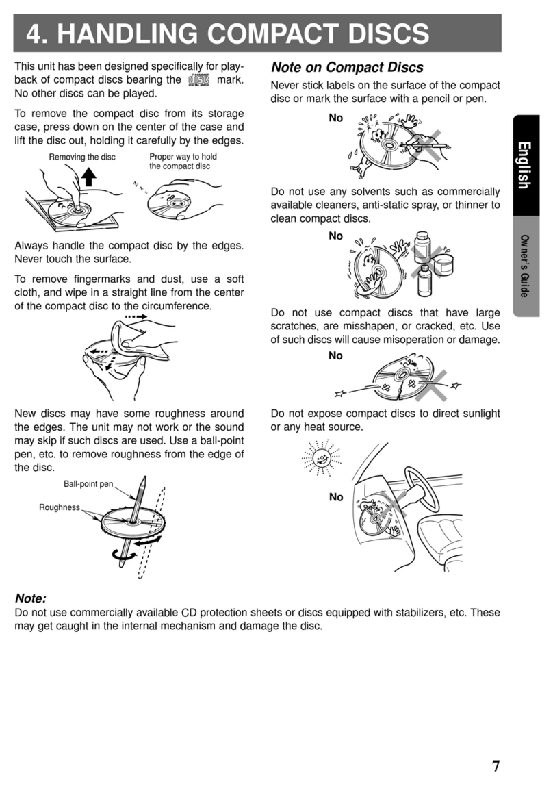
signal
[0
[ests
vromsin
cna
ia
Reset
signal!
input
(reset
at
“L”)
a3
37
i=)
>
i
P10(CLK)
FL
drive
power
supply
(connected
to
—33V)
Vv
=
—
>
QO
Ss
n
<
z
oO
FL
grid
signal
(Not
used,
open)
13(RECV)
uv
—
a
uu
Uv
mel
Pe
|
a
|
ae
wo
+
D
G
Sub-code
block
(Q
data)
clock
(75Hz)
input
(Not
used,
open)
IRQ/TC1
Key
return
signal
18
n
Sub-code
frame
clock
(7.35kHz)
uy
(Not
used,
open)
Sub-code
Q
data
input
(Not
used,
open)
nD
=
Uv
=n
So
Key
scan
signal
(Not
used,
connected
to
+5V)
np
Bm
U
23
8
Ea
bid
Oo
FL
anode
signal
31
42
@
MN6623
(Digital
Filter
and
D/A
Converter)
Command
Ioad
input
(load:
L)
Reset
signal
input
(reset
at
“L”)
2S
select
terminal
(“H”
=I?S)
vo
Division
|
Division
Ce
a
se
Ce
oc
fons:
[1
[emma
aen
|
[e[eseowen
T—
feseceee
fastens
|ovooz
=|
1
|
Power
supply
(connected
to
+5V)
joss
[1
[ete
wai
[inser
fence
fanaa
[a
[awe
aie
384
fs
(16.9344
MHz)
output
ibe
|
Power
down
terminal
TEST
terminal
(Not
connected)
[eoienm
|
Lch
data
output,
(+)
terminal
nN
ph
oO
>
N
~s
o
ND
~
on
~
~N
fog
o
~~
a
wo
>
a
=i
4
=
36
37
z
z
z
4
4
Lwd
OUTL(—)
14
17
8
1
41
Command
data
input
Command
clock
input
‘|
Q406
DTCI24ES
TRANS!
STOR
‘|
Q803
2SD1450RS
TRANS!
STOR
SL-P250
Mi
REPLACEMENT
PARTS
LIST
(Electrical
parts)
Notes:
*
Important
safety
notice
:
Components
identified
by
A\
mark
have
special
characteristics
important
for
safety.
When
replacing
any
of
these
components
use
only
manufacturer’s
specified
parts.
*
Bracketed
indications
in
Ref.
No.
columns
specify
the
area.
(Refer
to
the
first
page
for
area.)
Parts
without
these
indications
can
be
used
for
all
areas.
*
M
Indicates
parts
that
the
supplied
by
MESA.
*
“©®"
mark
parts
are
used
for
silver
type
only.
*
“@®"
mark
parts
are
used
for
black
type
only.
Parts
other
than
“©”
and
“©”
marked
are
used
for
both
silver
and
black
types.
fy
Cl
INTEGRATED
CIRCUITS
9)
SVDISR35200A
=
RECTIFIER
tcl
LM2940T5
|.C,
REGULATOR
04
A
SVDISR35200A
RECTIFIER
1C13
SVIBA4558FT1
—1.C,
REGULATOR
Ds
=
AN
SVDISR35200A
«RECTIFIER
1C101
AN8370S
1.C,
OPTICAL
SERVO
DIG
MA4330M
DIODE
C102
MN6636
1.C,
ANALOG
SW.
7A
SVDISR35200A_
«RECTIFIER
1C103
AN6554NS
1.C,
OPERATION
AMP.
DI8
MA4062
DIODE
1C104
AN6552S
|.C,
OPERAT
|
ON
AMP.
o21
AA
SVDISR35200A
RECTIFIER
10105
AN6552S
1.C,
OPERATION
AMP.
D2
AM
SVDISR35200A
=
RECTIFIER
1106
AN6552S
1.C,
OPERATION
AMP.
023
MA4062-H
DIODE
10201
LM2340TS
1.C,
REGULATOR
D181
MAI65
DIODE
1202
AN6552S
1.C,
REGULATOR
D182
MA165
DIODE
1C301
MN6617S
1.C.
SIGNAL
PROCESSING
D183
MAI65
DIODE
10302
SVICXKS5S16M
—-1.C,
16K
RAM
D184
MA165
DIODE
10401
MNIS54PEP
1.C,
SYSTEM
CONTROL
0201
MA4056-M
DIODE
1402
SVIBA4558FT1
—1.C,
OPERAT1ON
AMP,
0401
MAI65
DIODE
1C501
AN8371S
1.C,
DATA
SLICE/PLL
0410
MA4033M
DIODE
1C601
MNIS261PEN
—1.C,
FL
DRIVE
D411
MAI65
DIODE
(C602
HC~MD10E
1.C.
REMOTE
SENSOR
D601
MA165
DIODE
(E,
EK,
XL,
EG)
pe02
MA165
DIODE
(EB.
EH,
EF)
D603
MAI65
DIODE
(EI,
XA,
XB)
604
MAI65
DIODE
(PA,
PE,
PC}
D606
MAI65
DIODE
1ce02
HC-MD12M
1.C,
REMOTE
SENSOR
0607
MAI65
DIODE
{M,
MC}
D608
MAI65
DIODE
1C801
MN6623
1.C.
D/A
CONVERTER
D609
MAI65
DIODE
1c802
SVINJM4560M
—-1.C,
OPERAT1ON
AMP.
D610
MAI65
DIODE
1C803
SV
1
LM83GM
1.C,
OPERATION
AMP.
D851
MAI65
DIODE
(C804
SV1NJM4560M
—1.C,
OPERAT!ON
AMP.
0852
MAI65
DIODE
1C805
SVIHBON2175.—s1.C,
LPF
MAI65
DIODE
MA165
DIODE
SV1H8DN2175
1.C,
LPF
M5218L
1.C,
HEADPHONES
AMP.
A
(EK,
XA,
XB)
(PA.
PE,
PC)
1C2
Ay
SRUF38
1.C.
PROTECTOR
SRUF38
1.C,PROTECTOR
2SB1240-P
TRANSISTOR
Qala
2SB12380S
TRANSISTOR
aig
2SD1862-P
TRANS!
STOR
Qtol
2SA1547-0
TRANSISTOR
(EK,
XA,
XB}
Qi4i
2SD1862-P
TRANSISTOR
(PA,
PE,
PC)
Q142
2SB1240-P
TRANSISTOR
ICPI1
AN
SRUNI5
|.C.PROTECTOR
Ql61
2SD1862-P
TRANSISTOR
(EK}
Qlé2
2SB1240-P
TRANSISTOR
ICPI2
AN
SRUNI5
1.C,PROTECTOR
Qisi
2SD1862-P
TRANSISTOR
(EK)
Q182
2SB1240-P
TRANS!
STOR
Q201
2SD1862-P
TRANSISTOR
203
2SD1862-P
TRANSISTOR
Q301
DTC124ES
TRANSISTOR
36)
DTAI24EST
TRANSISTOR
Q401
2SD1862-P
TRANSISTOR
Q4pe
2881240-P
TRANS
|
STOR
0403
28D1962-P
TRANS1
STOR
Q404
2SB1240-P
TRANS!
STOR
VARIABLE
RESISTORS
EVNDSAA00B53
~—«V.R,
BEST
EYE
ADJ.
VR102
EVNDSAA00B14_—-V.R,
TR
GAIN
ADJ.
VR103
EVNDSAA00BI4
~—-V.R,
TR
OFFSET
ADJ.
VR104
EVND3AA00B14
=
V.R,
FO
GAIN
ADJ.
VR106
EVNDSAA00B14
—-V.R,
FO
OF
FSET
ADJ.
VR106
EVNDSAA00BS3_~—s«V.R,
TR
BALANCE.
ADJ.
VRS501
EVND3AA00B13
VR,
PLL
ADJ.
VR871
EVUNIAQISAIS
—
V.R.
HEADPHONES
LEVEL
MAGNET
RESISTOR
ELEMENTS
RAI
EWS7LOA00Q53
RESISTANCE
UNIT
L871
ELEPK1ROKA
COIL
L872
ELEPKIROKA
COIL
L873
ELEPKIROKA
COIL
1
A
SLTD5KOG5SC
=
POWER
TRANSFORMER
{M,
MC)
11
A
SLTD5KO66SE
=
POWER
TRANSFORMER
(E,
EG,
EB.
EH)
(EF.
£1)
T1
A
SLTDS5KO67SG
=
POWER
TRANSFORMER
801
28C3311A-Q
TRANSISTOR
Q3802
2S8C3311A-Q
TRANS!
STOR
3804
2SD1450RS
TRANS
1
STOR
851
DTAI24EST
TRANSISTOR
852
DTC124ES
TRANSISTOR
0853
DTANA4EST
TRANSISTOR
854
DTCI24ES
TRANS!
STOR
855
DTAI24EST
TRANS
STOR
Q861
28C3311A-Q
TRANS1
STOR
Qe62
2SA1309Q.RS
TRANS!
STOR
2SD1450RS
TRANSISTOR
2SD1450RS
TRANSISTOR
A
A
SVD1SR35200A
SVD1SR36200A
RECTIFIER
RECTIFIER
SSPDI8
SW,
LOADING
DET.
$601
EVOQS405K
SW,
OPEN/CLOSE
se0e
EVQQS405K
Sw,
STOP
$603
EVQQS405K
SW.
PAUSE
$604
EVQQS405K
SW.
PLAY
$605
EVQQS405K
SW,
REPEAT
S606
EVQQS405K
SW,
PROGRAM
$607
EVQQS405K
SW,
R.SEARCH
$608
EVQQS405K
SW,
F.SEARCH
$609
EVQQS405K
SW,
R.
INDEX
S610
EVQQS405K
SW.
F.
INDEX
S61)
EVQQS405K
SW.
EDIT
$612
EVQQS405K
SW.
TIME
$613
EVQQS405K
SW.
NUMER!
C(O)
S614
EVQQS405K
SW,
NUMER
1
C(3)
S615,
EVQQS405K
SW,
NUMER
|
C(2)
S616
EVQQS405K
SW.
NUMERIC)
S617
EVQQS405K
SW,
NUMERIC(
+10)
$618
EVQQS405K
SW,
NUMER
1
C(6)
$619
EVQQS405K
SW.
NUMER
I
C(5)
$620
EVQQS405K
SW,
NUMER
I
C(4)
$621
EVQQS405K
SW.
NUMER
|
C(9)
$622
EVQQS405K
SW,
NUMER
i
C(8)
EVQQS405K
SW.
NUMERIC(7)
(XA,
XB,
PA)
(PE,
PC)
OSCILLATORS
X60!
$vQ49Us38S
OSCILLATOR
DISPLAYS
FLEOI
SADI2BT2IGK
DISPLAY
FUSES
FLAN
(E.
EK,
XL,
EG)
LEB,
EH,
EF)
(El)
FLAN
XBA2CO25TBOS
—
FUSE(250V.T250mA)
(XA,
XB,
PA)
(PE,
PC)
SWITCHES
Ss}
A
ESBE249V
SW,
POWER
so
A
SSRI87-1
SW,
VOLTAGE
SELECTOR
(XA,
XB,
PA)
(PE,
PC)
Si0l
SSPD17
SW,
LOADING
DET,
XBA2COI2TBOS
—
FUSE(250V.T125mA)
[rare
[rae
[ome
PACKING
MATERIAL
INSTRUCT
1ON
MANUAL
Pl
®
SPNO290
CARTON
BOX
(M,
E,
EG
EB)
S$QX54602
INSTRUCT
ION
MANUAL
(EH,
£1.
EK)
(XL,
XA,
XB}
SQX54603
INSTRUCT
ION
MANUAL
(PA,
PE,
PC)
Pl
9)
SPND231
CARTON.
BOX
SQX54604
tNSTRUCT
1
ON
MANUAL
(MC)
PI
®
SPND292
CARTON
BOX
SFDAC0S5G02
POWER
CORD
(EF)
PI
©
SPND303
CARTON
BOX
SJA168
POWER
CORD
(E,
EG,
EB,
EH)
(E},
EK,
Xt}
SJAIT2
POWER
CORD
SPND304
CARTON
BOX
SJAI73
POWER
CORD
SPSD150
PAD
SPSD151
PAD
SUAITS-1
POWER
CORD
XZBS5X40A01
PROTECTION
BAG(UNIT)
(M)
sPSD152
CARTON
BOX(ACCESSOR
ES)
SJA183
POWER
CORD
XZB26X17CO3_
PROTECTION
BAGICORDS)
(xB)
XZBI0X26B05S
PROTECT
1
ON
BAG(REMOTE
CONT.)
A2
SJAI87
POWER
CORD
(E,
EG
EB,
EH)
(EF,
E1)
INSTRUCT
(ON
MANUAL
a
OA
RUPI20ZBS-H
AC
PLUG
ADAPTOR
(XB,
XA,
PA)
INSTRUCT
I
ON
MANUAL
ie
Pe)
A4
SJP2249-1
OUTPUT
CORD
INSTRUCT
|
ON
MANUAL
AS
UM-4NE
BATTERY
(E,
EG
EB,
EH
ENSTRUCT
ION
MANUAL
(EF,
El,
EK)
XL,
XB,
XA
INSTRUCT
I
ON
MANUAL
ie
PE
ee
AS
BATTERY
(M,
MC)
SL-P250
SE
4010)
PACKING
¢
F.B.
Ass’y
F.B.
Ass’y
P4
Mi
RESISTORS
AND
CAPACITORS
Notes:
*
Important
safety
notice
:
Components
identified
by
A\
mark
have
special
characteristics
important
for
safety.
When
replacing
any
of
these
components
use
only
manufacturer’s
specified
parts.
*
Bracketed
indications
in
Ref.
No.
columns
specify
the
area.
(Refer
to
the
first
page
for
area.)
Parts
without
these
indications
can
be
used
for
all
areas.
Numbering
System
of
Resistor
Resistor
Type
a
Example:
‘
Hen
:
:
:
Baie
+
Metal
Oxide
:
:
EBD
—%__
postic
vie
ee
202
:
Fuse
Type
Metal
é
18:
1/8W
Type
Wattage
Shape
Tolerance
Value
:
Metal
Film
:
>
V2W
(1/4W)
(1KQ)
:
Carbon
(chip)
:
50:
1/2W
ERX
2
AN
J
471
:
Metal
Film
(chip)
t
3A:
3W
Type
Wattage
Shape
Tolerance
Value
;
Solid
:
8G:
BW
(2W)
(470Q)
:
Incombustible
/
Box-Shaped
:
Wire-Wound
Numbering
System
of
Capacitor
:
Cip
Resistor
Example:
,
Cip
Resistor
Type
Voltage
Value
Tolerance
Peculiarity
Capacitor
Type
Voltage
Tolerance
(50V)
(0.001pJF)
:
Electrolytic
OJ
:
6.3V
:
K:
£10%
ECEA
50
M
330
:
Ceramic
1C
:
16V
:
M:
£20%
a
a
A
:
ic
C.
it
1H:
50V
.
+805
Type
Voltage
Pecliarity
Value
'
pale
epeen
es
5
SBV
;
ra
;
‘%
50V)
(33pF)
:
Poyester
4 :
-2
(
:
Polypropylene
2H
:
500V
:
J:
£5%
:
Ceramic
1
:100V
:
G:
£2%
:
Non
Polar
Electrolytic
KC
:
400V
AC
F:
21%
@
Capacity
are
in
microfarads
(UF)
unless
specified
:
Ceramic
(Chip
Type)
KC
:
125V
AC
C:
£0.25pF
otherwise,
P=
Pico-farads
(pF)
Ff
=Farads
(F).
:
Ceramic
(Chip
Type)
(UL)
D:
t0.5pF
@
Resistance
are
in
ohms
(Q),
unless
specified
:
Semiconductor
otherwise,
1K
=
1,000,
1M=
1,000kQ
:
Liquid
electrolyte
double
layer
capacitor
fem
[owe
[ve
[oe
[ow
[wm
[mm
[ove
[vom
ERJ6GEYJ270V
1/10
ERJGGEYJI03V
10K
1,10
ERDSOTJIOI
4
R154
ERJ8GEY
J3R3V
a9
1/8
R230
ERJ6GEYJ223V
22K
1/10
R13
ERDS2T
J103
WOK
1/4
R161
ERJ6GEYJ333V.
3K
O/10.
R231
ERJ6GEYJ273V
27K
_~=—«1/10
R14
ERDS2TJ163
10K
1/4
R162
ERJ6GEYJ222V
2.2K
1/10
R282
ERJ6GEYJ681V
680
1/10
R15
ERDS2TJ331
30
4
R163
ERJ6GEYIS33V
33K
1/10
R233
ERJ6GEYJ471
=
470-—s:'1/10
RIG
ERDS2T
J102
1K
1/4
R164
ERJOGEYJ153
15K
1/10
R301
ERDS2TJ472
4.1K
1/4
RIG
ERDS2T
471
4701/4
R165
ERJ6GEYJ122
1.2K
«1/10
R302
ERDS2T
J472
47K
1/4
RIT
ERDS2TJ471
410
1/4
R166
ERJ6GEYJ102V.
1K
1/10
R303
ERDS2T
472
4.7K
1/4
Rid}
ERJ6GEYJ154V.
-150K1/10
R67
ERJ6GEYJ681V
680
1/10
R304
ERDS2T
J472
4.1K
1/4
R102
ERJ6GEYJ472V
4.7K
1/10
R168
ERJ6GEYJ27T2V
2.7K
1/10
F305
ERDS2T
J472
4.7K
1/4
R103
ERU6GEYJ472V
4.7K
1/10
R169
ERJ6GEYJ392V.
3.9K
1/10
R307
ERDS2T
J104
100K
1/4
R104
ERJGGEYJ223V
22K_~=—s1/10
R170
ERJ6GEY
J101
100
«1/10
R308
ERDS2T
J561
560
1:4
R105
ERJ6GEYJ334V.
330K.
O1/10
R71
ERJ6GEYJ270V
27
~—s1/10
R309
ERDS2T
J472
47K
14
R107
ERJ6GEYJ473V.
47K—s1/10
Ri72
ERJ8GEYJ3R3V
3.3
«1/8
R310
ERDS2T
J222
22K
14
R108
ERJ6GEYJS32V.
3.3K
1/10
R180
ERJ6GEYJ474V
470K
1/10
R3It
ERDS2T
J472
4.1K
1/4
R109
ERJ6GEYJ822
8.2K
1/10
R181
ERJ6GEY
J471
470
1/10
R312
ERDS2T
J4R7
47
4
R110
ERJ6GEYJ682V
6.8K
1/10
Rt82
ERJ6GEYJ564V
560K
1/10
R313
ERDS2T
J4R7
47
W4
RW
ERJOGEYU682V.
6.8K
(1/10
R183
ERJ6GEYJ564V
560K
(1/10
R314
ERDS2T
J182
1.8K
1/4
R12
ERJ6GEYJ822
82K
1/10
R184
ERJ6GEYJ223V
22K
1/10
R361
ERDS2TJ103
10K
«1/4
RiI3
ERJ6GEYJ152V.
1.5K
1/10
R185
ERJ6GEYJ473V
47K
1/10
R362
ERDS2T
J334
SOK
«1/4
R14
ERJ6GEYJ152V.
1.5K
1/10
R186
ERJ6GEYJ473V)
47K
1/10
R353
ERDS2T
J123
12K
1/4
R15
ERJ6GEYJ102V.
1K
1/10
R187
ERJ6GEYJ473V)
47K
1/10
RQ54
ERDS2T
J274
270K
«1/4
RIG
ERJGGEYJ182V.
1.8K
(1/10
R188
ERJ6GEYJ473V
47K
=
1/10
R355
ERDS2T
J333
SOK
oO/4
RINT
ERJ6GEYJ182V.
1.8K
1/10
R191
ERJ6GEYJ154V
150K
1/10
R356
ERDS2T
J333
BK
O/4
R118
ERU6GEYU102V.
1K
1/10
R192
ERJ6GEYJ&24V
820K
«1/10
R367
ERD25FVJ8R2
8.2/4
R119
ERJ6GEYJ471
470
1/10
R193
ERJ6GEYJ101
1001/10
R404
ERDS2T
J221
220
«1/4
R120
ERJ6GEYJ120V.
12
=
1/10
RI94
ERJ6GEYJ683V
68K
1/10
R402
ERDS2T
221
220
«1/4
R122
ERJ6GEYU471
470~—s«*1/10
R195
ERJ6GEYJ103V.
10K
=—1/10
R403
ERDS2T
J221
2201/4
R123
ERJ6GEYJ393V
SOK
1/10
RIS
ERJ6GEYJ103V.
«10K
1/10
R404
ERDS2T
J221
220
«1/4
R14t
ERJ6GEYJ102V
1K
1/10
R197
ERJ6GEYJ473V
47K
1/10
R405
ERDS2TJ221
220
«1/4
R142
ERJ6GEYJ333V.
33K
—s/10
R198
ERJ6GEYJSS3V.
38K
1/10
R406
ERDS2T
J221
220
«1/4
R143
ERJ6GEYJ124V.120K_s«1/10
R199
ERJ6GEYJ473V
47K_—s1/10
R407
ERDS2T
J223
220
«(1/4
R144
ERJ6GEYJ333V
33K~—s«i/10
R201
ERJ6GEYJ102V.
1K
~~
1/10
R408
ERDS2T
J221
220
«1/4
R145
ERJ6GEYJ153
15K
1/10
R202
ERJ6GEYJ103V.
10K
_~=—1/10
R409
ERDS2T
J472
4.7K
1/4
R146
ERJ6GEYJ122«1.2K_—s«+1/10
R203
ERJ6GEYJ102V.
1K
=
1/10
R410
ERDS2T
J472
4.7K
1/4
R147
ERJ6GEYJ682V
6.8K
1/10
R204
ERJ6GEYJ682V
6.8K
1/10
Rall
ERDS2T
J472
4.1K
1/4
R148
ERU6GEYJ104V.
100K_s1/10
R205
ERJ6GEYJ682V
6.8K
1/10
R412
ERDS2T
472
4.7K
1/4
R149
ERJ6GEYJ152V.
1.5K
1/10
R207
ERJ6GEYJ474V
470K
(1/10
R413
ERDS2T
472
4.7K
1/4
R150
ERJ6GEYJ103V.
10K
=
=-1/10
R208
ERJ6GEYJ680V
681/10
R414
ERDS2T
J472
4.7K
1/4
R151
ERJ6GEYJ101
100
1/10
R214
ERJ6GEYJ471
470s
1/10
Rats
ERDS2T
J472
47K
1/4
ERJ6GEYJ331
=
330s
1/10
ERJ6GEYJ101
=—100-—-1/10
ERDS2TJ472
ERDS2TJ472
1/4
V4
ERJ6GEYJ153
15K
1/10
ERDS2T
J472
ERDS2TJ472
ERDS2T
J472
ERDS2T
J913
ERDS2TJ913
ERDS2T
J124
ERDS2T
J124
ERDS2TJ101
ERDS2TJ101
ERDS2T
J472
ERDS2T
J472
ERDS2T
J101
ERDS2TJ153
ERDS2T
J393
ERDS2T
J102
ERJ6GEYJ104V
ERJ6GEY
J562
ERJ6GEYJ474V
ERJ6GEYJ101
ERJ6GEYJ104V
ERJ6GEYJ333V
ERJ6GEYJ102V
ERDS2T
J472
ERDS2T
J472
ERDS2T
J472
ERDS2TJ472
ERDS2T
J472
ERDS2TJ103
ERDS2TJ103
ERDS2TJ105
ERDS2TJ103
ERDS2TJ103
ERDS2TJ103
ERDS2T
J103
ERDS2T
J273
ERDS2TJ273
ERDS2T
J273
ERDS2TJ273
ERDS2T
J473
ERDS2T
J473
ERDS2TJ473
ERDS2T
J473
ERDS2T
J221
ERDS2T
J221
ERDS2TJ474
ERDS2TJ474
ERDS2T
J104
ERDS2TJ104
ERDS2TJ681
ERDS2TJ681
ERDS2TJ473
ERDS2TJ473
ERDS2TJ331
ERDS2TJ121
ERDS2TJ121
ERDS2TJ104
ERDS2TJ104
ERDS2T
J222
ERDS2T
J331
ERDS2TJ105
ERDS2T
J105
ERDS2TJ102
ERDS2TJ471
ERDS2TJ104
ERDS2T
J683
ERDS2TJ102
ERDS2T
J102
ERDS2T
J102
ERDS2T
J102
ERDS2TJ102
ERDS2TJ102
ERDS2T
J103
ERDS2TJ103
ERDS2T
J473
ERDS2T
J473
ERDS2T
J121
ERDS2T
J12t
ERDS2TJ103
ERDS2T
J103
ERDS2T
J222
ERDS2T
J222
ECKDKC103PF2
ECKMIHIO3ZFX
ECKMIH103ZFX
ECEA1CU222
ECEA1CU222
ECEAIVU101
ECEAIAK101
ECEAIAK101
ECEAQJK470
ECEAICUS31
ECEAICUS31
ECEAIVUI01
ECEAICU221
ECFRIE104ZF5
RCUVIE104ZF
RCUVIHI02KB
RCUVIHIO2KB
RCUV1H681K
RCUVIHA7IKB
RCUV1H471KB
RCUV1H220KC
ECEAIHKKORI
ECEAIHKKO10
ECQVIH104J5Z
ECEAIAKK100
ECEATAKK100
ECEATHSNO10
RCUV1H182KB
RCUV1H682KB
RCUVIESS3KB
RCUV1H221KB
ECEAIHKKOI0
ECEAQJKS2201
RCUV1H681K
RCUV1E103KB
RCUVIHIOIKC
RCUV1HIO1KC
ECEAOJKS2201
ECEAQJKS470
RCUVIH102KB
RCUVIHI02KB
RCUV1H68IK
RCUV1E153KB
RCUV1H122KB
ECUVIE473KB
ECEAIVSN2R21
ECEATHSNR22
RCUV1E153KB
RCUVIHE81K
RCUV1E103KB
ECEAIESNSR3i
ECEAIHSNORI
ECQV1H474J2Z3
RCUV1H221KB
RCUV1H68&2KB
ECEAIHSNO10
ECUVIC224KR
RCUV1E103KB
ECEAQJKS1011
ECEAOJKAI01B
ECEAQJKA101B
RCUV1E104ZF
RCUV1E104ZF
RCUVIE104ZF
ECUV1E823KB
ECUVIE473KB
ECFRIE104ZF5
ECBT1C103NS
ECFRIE104ZF5
0.01
125
0.01
50
0.01
2200
100
100
100
41
RC)
*%0
100
220
01
2
01
2
0.001
50
0.001
50
680P
50
470P
50
470P
50
22P
50
0.1
50
1
50
0.1
50
10 10
10 10
1
80
0.0018
50
0.0068
50
0.083
25
220P
50
1
50
2
63
680P
50
0.01
25
100P
50
100P
50
2
63
47
63
0,001
50
0.001
50
680P
50
0.015
25
¥200P
50
0,047
25
22
3
0.22
50
6B0P
50
33
25
0.1
50
220P
50
0.0068
50
1
0.22
16
0.01
2
100
63
100
63
0.1
2%
01
25
01
2
0.082
25
0.047
25
01
2
0.1
ECEAOJK101
ECFRIE104ZF5
ECFRIE104ZF5
ECBT1C103NS
ECFRIE104ZF
ECBT1H102KB
ECEAQJK470
ECFRIE104ZF5
ECFRIE104ZF5
ECFRIE104Z2F5
ECBT1H102KB
ECBTIHI02KB
ECEAIHKNO10
ECUVIE104KB
ECQVIH104UZ
ECEATAKK100
RCUVIE104ZF
RCUVIE104ZF
RCUVIHI50K
RCUVIH1I02KB
ECEAIASN100
RCUVIHIO0DC
ECUVIE104KB
ECEAIHKSR47
RCUV1HE81K
RCUV1H681K
ECUVIC224KR
RCUV1IE153KB
ECEAIVSN2R21
RCUV1H471KB
ECUV1C224KR
RCUV1H472KB
ECBT1H223Z2F
ECEAOJK470
ECBT1E223ZF
ECBT1E223ZF
ECBT1H680J
ECBT1H680J
ECBT
1H680J
ECBTIH680J
ECBT1H470J5
ECBT1H470J5
ECBT1H470J5
ECBT1H470J5
ECEAIENSR3S
ECEAIENSR3S
ECBT1H102KB
ECBT1H102KB
ECEAICN220S
ECEATCN220S
ECBT1H102KB
ECBT1HI02KB
ECBT
1HSR6K5
ECBT1HSR6K5S
ECEAICN220S
ECEAICN220S
ECFRIE104ZF
ECEA0JS331
ECEA0JS331
ECEAQJU471
ECEAQJS331
ECEATHKN2R2B
ECFRIE104ZF5
ECFRIE104ZF5
ECFRIE104ZF5
ECFRIE1O4ZF5
ECFRIE104ZF5
ECFRIE104ZF5
ECEATAK101
ECEAIAK101
ECBT1E223ZF
ECBT1E223ZF
ECBT1E103ZF
ECBTIE103ZF
ECBTIE103ZF
ECEAIAKN100B
ECEA1AKN100B
@
PRINTED
To
Servo
Gain
Adjuster
Dy
(|;
NE
Ep
SSRRRPRPSSRRRRRKKES:
;e
Components
use
only
K
vam7g|s
rm
M:
£20%
2:
:£10%
+
BO
%
:£5%
:
£a%
:£1%
:
£0.25pF
:
£0.5pF
ERDS2TJ472
4.7K
R419
ERDS2T
472
4.1K
1/4
R420
ERDS2TJ472
47K
1/4
R421
ERDS2T
913
91K
1/4
R422
ERDS2TJ913
SIK
1/4
R423
ERDS2T
J124
120K
1/4
R424
ERDS2T
J124
120K
1/4
R425
ERDS2TJ101
1001/4
R426
ERDS2TJ101
100
1/4
R427
ERDS2T
J472
4.7K
1/4
R431
ERDS2T
J472
4.7K
1/4
R4g2
ERDS2T
J101
100
1/4
R433
ERDS2T
J153
1SK
1/4
R434
ERDS2T
5393
3K
1/4
R435
ERDS2T
5102
iK
1/4
R501
ERJ6GEYJ104V
100K
1/10
R502
ERJ6GEYJ562
5.6K
1/10
R503
ERJ6GEYJ474V
470K
1/10
R504
ERJ6GEYJ101
=
100-—«‘1/10
R505
ERJ6GEYJ104V
100K
1/10
R506
ERJ6GEYJ333V
33K
1/10
R507
ERJ6GEYUI02V
1K
=
1/10
R60i
ERDS2T
J472
4.1K
1/4
R602
ERDS2T
J472
4.7K
1/4
R603
ERDS2T
J472
4.7K
1/4
R604
ERDS2TJ472
4.1K
1/4
R605
ERDS2T
J472
4.1K
1
R607
ERDS2TJ103
WOK
1/4
R608
ERDS2T
J103
1OK
1/4
R6I3
ERDS2T
J105
IM
1/4
R801
ERDS2TJ103
10K
1/4
Re2
ERDS2TJ103
10K
1/4
R803
ERDS2T
J103
10K
1/4
R804
ERDS2TJ103
10K
1/4
R805
ERDS2T
J273
27K
1/4
R806
ERDS2T
J273
27K
1/4
R807
ERDS2T
J273
2mK
1/4
R808
ERDS2T
J273
27K
1/4
R803
ERDS2T
J473
47K
1/4
R810
ERDS2T
473
41K
1/4
R811
ERDS2TJ473
47K
1/4
R812
ERDS2T
J473
41K
1/4
R813
ERDS2T
J221
220
1/4
R814
ERDS2TJ221
220
1/4
R815
ERDS2T
J474
470K
1/4
RBI6
ERDS2TJ474
410K
1/4
R817
ERDS2T
J104
100K
1/4
R818
ERDS2T
J104
OOK
1/4
R819
ERDS2T
J681
680
1/4
R820
ERDS2T
J681
6801/4
R821
ERDS2TJ473
47K
1/4
R822
ERDS2TJ473
41K
1/4
R823
ERDS2TJ331
330
«1/4
R&24
ERDS2TJ121
120,
1/4
R825
ERDS2TJ121
120
1/4
R826
EROS2TJ104
100K
1/4
R827
ERDS2TJ104
100K
1/
R831
ERDS2T
J222
2.2K
1/4
R840
ERDS2TJ331
30
1/4
R641
ERDS2T
J105
iM
1/4
R842
ERDS2T
J105
IM
1/4
ERDS2TJ121
R877
ERDS2TJ103
WOK
1/4
R878
ERDS2TJ103
10K
1/4
R879
ERDS2T
J222
2.2K
1/4
ERDS2T
J222
C306
ECEAQJK101
100
63
C307
ECFRIEIO4ZF5
(0.1
25
C308
ECFRIEI4ZF5
01
2
C303
ECBTICIO3NS
§=0.01_
16
C310
ECFRIEIO4ZF
90.1
C351
ECBTIHI02KB
0,001
50
C401
ECEAQJK470
47
63
C402
ECFRIEIO4ZF5
0.1
25
C403
ECFRIEIO4ZF5
0.1
2%
C404
ECFRIEIO4ZF5
0.1
25
C405
ECBTIHI02KB
0.001
50
C406
ECBTIHIQ2KB
0.001
50
C407
ECEAIHKNOIO
3861)
=
«450
C501
ECUVIEI04KB
0.1
25
C802
ECQVIH104UZ
0.1
50
C§03
ECEAIAKK100
«10
«10
C504
RCUVIEIO4ZF
=
0.15
C05
RCUVIEIO4ZF
=
O.t
5
C506
RCUVIHI50K
1SP
50
C807
RCUVIHIO2KB
=
0.001
50
C508
ECEAIASNIO0
=
10s
110
C509
RCUVIH100DC
~=—s«10P_—s«
5
C510
ECUVIEID4KB
0.125
C$11
ECEAIHKSR47
=—0.47_-50
C512
RCUV1H681K
680P
50
C513
RCUV1HO8IK
680P
50
C514
ECUVIC224KR
022
16
C515
RCUVIEISSKB
=
0.015
25
C516
ECEAIVSN2R21
2.2
35
C517
RCUVIH471KB
470P_
50
C519
ECUVIC224KR
0.22
“16
C820
RCUVIH472KB
—0,0047
50
C601
ECBTIH223ZF
0.022
50
C602
ECEAQJK470
47
63
C603
ECBTIE223ZF
0,022
25
C604
ECBT1E223ZF
0.022
25
C801
ECBT1H680J
68P
50
C802
ECBT1H680J
68P
50
C803
ECBT
1IH680J
68P
50
C804
ECBT1H680U
68P
50
C805
ECBTIH470J5
47P
50
50
50
50
ECKDKCI03PF2
0.01
125
C2
A
ECKMIHIO3ZFX
0.01
50
C3
A
ECKMIHI03ZFX
0.01
50
C10
ECEAICU222
2200
16
cil
ECEAICU222
2200
16
cle
ECEAIVUIOI
100
3%
C13
ECEAIAK101
100
10
C14
ECEAIAKIOI
100
10
Ci
ECEAQJK470
47
63
C6
ECEAICUS31
30
16
Ci?
ECEA1CUS31
®0
16
C18
ECEAIVUI0I
100
3%
C2)
ECEAICU221
220
16
C30
ECFRIEIO4ZF5
0.1
25
C101
RCUVIEIO4ZF
=—0.1
25
C102
RCUVIHIO2KB
0.001
50
C103
RCUVIHI02KB
0.001
50
C104
RCUV1H681K
680P
50
C105
RCUVIHA71KB
=
470P_
50
C106
RCUVIH471KB
—
470P_-50
C107
RCUVIH2200KC
=
22P_—-
50
C108
ECEAIHKKORI
0.1
50
C108
ECEAIHKKOIO
«=i
050
CiH0
ECQVIHIO4JZ
0.1
50
ci
ECEAIAKK100
10
10
Cli2
ECEAIAKK100
10
10
C113
ECEAIHSNOIO.
=61
80
C114
RCUVIHI82KB
00018
50
C15
RCUVIH682KB
0.0068
50
CII
RCUVIESS3KB
0.083.
25
Cny7
RCUVIH221KB
—
220P
50
Cig
ECEAIHKKOIO
38610
CH
ECEAQJUKS2201
22
63
C120
RCUV1HE81K
680P
50
C121
RCUVIE103KB
0.0125
C22
RCUVIHIOIKC
=
100P_
50
C123
RCUVIHIOIKC
=
100P._-50
C125
ECEAQUKS2201
22
63
Cla
ECEAQJKS470
47-63
Cle
RCUVIH102KB
0.001
50
C128
RCUVIHIO2KB
0.001
50
Ct29
RCUV1H681K
680P
50
C14}
RCUVIEIS3KB
0.015
25
C142
RCUVIH122KB
=
1200P._
50
C143
ECUVIE473KB
0.047
25
C144
ECEAIVSN2R21
22
35
C145
ECEAIHSNR22
90.22
50
C161
RCUVIE15S3KB
0.015
25
C162
RCUVIH681K
680P
0
C163
RCUVIEI03KB
=
0.01.
25
C164
ECEAIESNSR31
3.3
25
C165
ECEAIHSNORI
0.1
50
Ci8t
ECQVIH474JZ3
0.47
50
C182
RCUVIH221KB
220P
50
C183
RCUVIHE82KB
0.0068
50
C806
ECBTIH470U5
=
47P
C807
ECBTIH470U5
—47P
C808
ECBT1H470U5
=
47P
C809
ECEAIENSR3S
=
3.325
c8t0
ECEATENSR3S
=
3.3025
C81
ECBTIHIG2KB
0.001
50
cal2
ECBTIHI02KB
0.001
50
C813
ECEAICN20S
22
16
C814
ECEAICN220S
22)
16
C815
ECBTIH102KB
0.001
50
C816
ECBTIHIO2KB
0.001
50
C822
ECBTIHSR6KS
§=65.6P
50
C824
ECBTIHSR6K5
5.6P
50
C830
ECEAICN2200S
22-16
C83)
ECEAICN20S
22
16
C840
ECFRIEIO4Z2F
=O.
25
C841
ECEA0JS331
300
6.3
C842
ECEAQJS331
30
6.3
C851
ECEAQJU471
410
63
C8&2
ECEA0JS331
30
63
R851
ERDS2TNI02
1K~—1/4
C853
ECEATHKN2R2B
22
50
R862
ERDS2TU471
4701/4
ap
PMC
e
i
me
cas4
ECFRIEIO4ZF5
0.1
25
REE
ERDS2TJ104
100K.
1/4
A
RCOMIEIES
tare
C855
ECFRIEIOAZF5S
0.1
25
R864
ERDS2TJ63GBKO/4
=
PLEADS
he
C856
ECFRIEIOAZF5
0.1
25
RB5S
ERDS2TJI02
1K
1/4
ee
EGEAMNOIEs
thoes
C857
ECFRIEIO4ZF5
0.1
25
R856
ERDS2TJI02
1K
1/4
be
ECEMMRIOIE..
Won
ca58
ECFRIEIOAZF5
01
25
R857
ERDS2TJ102
1K
1/4
oi
REOIEGUE:
once
C859
ECFRIEIOAZF5
0.1
25
Rasa
ERDS2TJI02
1K
1/4
oe
AGUIEIOE
ot
a
C861
ECEAIAKI01
100.10
PEGI
ERDS2TNI02
IK
1/4
i
neiVEWe:
See
862
ECEAIAKION
100-10
RBG
ERDS2TJI02
«IK
«41/4
on
ECUWVIERAE.
“Mie
ce7!
ECBTIE2232F
0,022
25
RBTI
ERDS2TJ103.
«10K
«1/4
is
EAMIENAE
lane
ca72
ECBTIE223ZF
0,022
25
RBI2
ERDS2TJ103.
«10K
1/4
ae
ECERIEIC
ERI
C873
ECBTIEIO3ZF
0.01
25
R873
ERDS2TJ473.
47K
1/4
Oe
ECOTICMGNS
“OM
3
ca74
ECBTIEIZF
0.01
25
RETA
ERDS2TU473.
47K
1/4
ECPRICICEee“s
C875
ECBTIEIOQZF
0,01
25
ERDS2TJ121
carl
ECEAIAKNIO0B
10 10
ECEAIAKNI00B
SL-P250
M@
PRINTED
CIRCUIT
BOARD
AND
WIRING
CONNECTION
DIAGRAM
To
Servo
Gain
Adjuster
AC
IN
ra
Power
Trans
former
E
|
POWER
SUPPLY
P.C.B.
POWER
MOTOR/SWITCH
P.C.B.
S!0)
(OPEN/CLOSE)
REMOTE
LINE
OUT
(Leh)
(Reh)
aa
LOADING
8
MOTOR
DiA
CONVERTER!
AUDIO
P.C.B.
$102
{OPEN/CLOSE
)
OPTICAL
PICKUP
[Eq
servo
p.c.s.
Resistance
Unit
CNIOL
SPINDLE
ioe
=
Hl
=e)
[zoom]
Fine
|p|
CNiIO2
CNIO3
Red
rk
CN606
HEADPHONES
AMP
P.C.B.
REMOTE
SENSOR
EY
oreration
p.c.s.
PHONES
PHONES;
LEVEL
SL-P250
SL-P250
SL-P250
1
2
3
4
5
6
7
8
9
10
PRINTED
CIRCUIT
BOARDS
[=]
SERVO
f
,
A
OPERATION
P.C.B.
REMOTE
B
Cc
MOTOR/
SWITCH
P.C.B.
D
LOADING
MOTOR
E
F
LINE
OUT
SL-P250
SL-P250
5 6
7
8 9
10
11
12
13
14
MOTORI
C
SWITCH
D
SPINDOL
MOTOR
LOADING
MOTOR
HEADPHONES
AMP
P.C.B.
PHONES
LEVEL
—31—
32
1
2018)
16
17
18
19
|
POWER
SUPPLY
P.C.B.
e
For
(M)
and
(MC)
areas.
(20V
60Hz)
Tt_(Power
transformer)
_
[Srower
SUPPLY
P.C.B.
e
For
(EK)
area.
(240V
50Hz)
Ti
(Power
transformer
)
SL-P250
20
21
22 23
24
[3
POWER
SUPPLY
P.C.B.
°
For
(E),
(EG),
(EB),
(EH),
(EF),
(Ei)
and
(XL)
areas.
ate
ees
TI
(Power
transformer
)
a
a
|
[3
POWER
SUPPLY
P.C.B.
e
For
(XA),
(XB),
(PA),
(PE)
and
VOLTAGE
SELECTOR
(PC)
areas.
($2)
(110/127/220/240V
50/60Hz)
LO
ee
ee

Other Technics CD Player manuals

Technics SL-PG340 User manual

Technics

Technics SL-PG340 User manual

Technics SL-PD947 User manual

Technics

Technics SL-PD947 User manual

Technics SLPD8 - COMPACT DISC CHANGER User manual

Technics

Technics SLPD8 - COMPACT DISC CHANGER User manual

Technics SL-PG470A User manual

Technics

Technics SL-PG470A User manual

Technics SL-EH50 User manual

Technics

Technics SL-EH50 User manual

Technics SL-PG590 User manual

Technics

Technics SL-PG590 User manual

Technics SL-C700 User manual

Technics

Technics SL-C700 User manual

Technics SL-PG480A - schematics User manual

Technics

Technics SL-PG480A - schematics User manual

Technics SLPG4 - COMPACT DISC PLAYER User manual

Technics

Technics SLPG4 - COMPACT DISC PLAYER User manual

Technics SL-P1000 User manual

Technics

Technics SL-P1000 User manual

Technics SL-PG440 User manual

Technics

Technics SL-PG440 User manual

Technics SL-PG350 User manual

Technics

Technics SL-PG350 User manual

Technics SL-PS900 User manual

Technics

Technics SL-PS900 User manual

Technics SL-EH760 User manual

Technics

Technics SL-EH760 User manual

Technics SL-PG480A - schematics User manual

Technics

Technics SL-PG480A - schematics User manual

Technics SL-E10 User manual

Technics

Technics SL-E10 User manual

Technics SL-C700 User manual

Technics

Technics SL-C700 User manual

Technics CQ-DP5EU/EC User manual

Technics

Technics CQ-DP5EU/EC User manual

Technics SLPD8 - COMPACT DISC CHANGER User manual

Technics

Technics SLPD8 - COMPACT DISC CHANGER User manual

Technics SL-DV290EE User manual

Technics

Technics SL-DV290EE User manual

Technics SL-P477A User manual

Technics

Technics SL-P477A User manual

Technics SL-P1200 User manual

Technics

Technics SL-P1200 User manual

Technics SL-XP600 User manual

Technics

Technics SL-XP600 User manual

Technics SL-PS770A User manual

Technics

Technics SL-PS770A User manual

Popular CD Player manuals by other brands

Panasonic DVD-L10 operating instructions

Panasonic

Panasonic DVD-L10 operating instructions

Denon DVM-2845CI operating instructions

Denon

Denon DVM-2845CI operating instructions

Sharp MD-MT877H Operation manual

Sharp

Sharp MD-MT877H Operation manual

Philips AX5011 quick guide

Philips

Philips AX5011 quick guide

NuTone IM-440 Series installation instructions

NuTone

NuTone IM-440 Series installation instructions

Aiwa XP-SR311AU Service manual

Aiwa

Aiwa XP-SR311AU Service manual

Hitachi CX77MP3C instruction manual

Hitachi

Hitachi CX77MP3C instruction manual

Pioneer CDJ-500II Service manual

Pioneer

Pioneer CDJ-500II Service manual

Sony CDP-C20 Service manual

Sony

Sony CDP-C20 Service manual

Kenwood KDC-C602FM instruction manual

Kenwood

Kenwood KDC-C602FM instruction manual

Integra DPC-5.2 Schematic diagram & printed circuit board view only

Integra

Integra DPC-5.2 Schematic diagram & printed circuit board view only

Sharp MD-MT99H Operation manual

Sharp

Sharp MD-MT99H Operation manual

Sony CFD-980 Operating Instructions  (English,... operating instructions

Sony

Sony CFD-980 Operating Instructions (English,... operating instructions

Sony CFD-922L Service manual

Sony

Sony CFD-922L Service manual

Sony S300 - CFD Boombox operating instructions

Sony

Sony S300 - CFD Boombox operating instructions

Philips AZ9211/00 user manual

Philips

Philips AZ9211/00 user manual

Onkyo DX-6630 Service manual

Onkyo

Onkyo DX-6630 Service manual

Optimus CD-3580 owner's manual

Optimus

Optimus CD-3580 owner's manual

manuals.online logo
manuals.online logoBrands
  • About & Mission
  • Contact us
  • Privacy Policy
  • Terms and Conditions

Copyright 2025 Manuals.Online. All Rights Reserved.