TEDIA PCD-8006 User manual
Digital I/O PCIe card
PCD-8006
User Guide

Manufacturing, sales office, service center, technical support and headquarters:
address: TEDIA®spol. s r. o.
Zábělská 12
31211 Plzeň
Czech Republic
website: http://www.tedia.eu
phone/e-mail: https://www.tedia.eu/contacts
tech. support: https://www.tedia.eu/support
Trademarks:
TEDIA is a registered trademark of TEDIA®spol. s r. o. All other trademarks or registered
marks in this manual belong to their respective owners.
Disclaimer:
This manual has been carefully reviewed for technical accuracy. In the event that technical or
typographical errors exist, TEDIA®reserves the right to make changes to subsequent editions
of this document without prior notice to holders of this edition.
TEDIA®provides this document “as is,” without warranty of any kind, either expressed or
implied, including, but not limited to, its particular purpose. TEDIA®reserves the right to make
improvements and/or changes to this manual, or to the products and/or the programs
described in this manual, at any time.
Information provided in this manual is intended to be accurate and reliable. The reader
should contact TEDIA®, if errors are suspected. In no event shall TEDIA®be held liable for any
form of damage arising out of or related to this document or the information contained in it.
Copyright © 1994÷2015 TEDIA®spol. s r. o., All rights reserved.
My DAQ Card Details:
type of card: . . . . . . . . . . . . . . . . . . . . . . . . . . . . . . . . . . (e.g. PCD-8006)
serial number: . . . . . . . . . . . . . . . . . . . . . . . . . . . . . . . . . . (e.g. 80010108)
purchase date: . . . . . . . . . . . . . . . . . . . . . . . . . . . . . . . . . .
card owner: . . . . . . . . . . . . . . . . . . . . . . . . . . . . . . . . . .

CE Declaration of Conformity, WEEE
1. Introduction
1.1 Description . . . . . . . . . . . . . . . . . . . . . . . . . . . . . . . . . . . . . . . . . . . . . . . . . . . I - 1
1.2 General instructions for use . . . . . . . . . . . . . . . . . . . . . . . . . . . . . . . . . . . . . . I - 1
1.3 Note on the contents of the manual . . . . . . . . . . . . . . . . . . . . . . . . . . . . . . . . I - 1
1.4 New firmware versions and customer´s firmware . . . . . . . . . . . . . . . . . . . . I - 1
2. Specifications
2.1 Digital ports . . . . . . . . . . . . . . . . . . . . . . . . . . . . . . . . . . . . . . . . . . . . . . . . . . . I - 2
2.2 Interrupt logic . . . . . . . . . . . . . . . . . . . . . . . . . . . . . . . . . . . . . . . . . . . . . . . . . I - 2
2.3 General data . . . . . . . . . . . . . . . . . . . . . . . . . . . . . . . . . . . . . . . . . . . . . . . . . . . I - 2
3. Installation
3.1 Introduction . . . . . . . . . . . . . . . . . . . . . . . . . . . . . . . . . . . . . . . . . . . . . . . . . . . I - 3
3.2 Hardware configuration . . . . . . . . . . . . . . . . . . . . . . . . . . . . . . . . . . . . . . . . . . I - 3
3.3 Installation . . . . . . . . . . . . . . . . . . . . . . . . . . . . . . . . . . . . . . . . . . . . . . . . . . . . I - 3
3.4 Location of switches and connectors . . . . . . . . . . . . . . . . . . . . . . . . . . . . . . I - 3
3.5 Connector pin assignment . . . . . . . . . . . . . . . . . . . . . . . . . . . . . . . . . . . . . . . I - 3
4. Digital Ports
4.1 Introduction . . . . . . . . . . . . . . . . . . . . . . . . . . . . . . . . . . . . . . . . . . . . . . . . . . . I - 4
4.2 Description of digital ports . . . . . . . . . . . . . . . . . . . . . . . . . . . . . . . . . . . . . . . I - 4
4.3 Interrupt logic . . . . . . . . . . . . . . . . . . . . . . . . . . . . . . . . . . . . . . . . . . . . . . . . . I - 4
Appendix - Tables and Figures
Notes
Table of Contents
PCD-8006 User Guide - Table of Contents
rev. 10.2015

CE Declaration of Conformity
All TEDIA®products described in this user guide comply with
the essential requirements of the following applicable
European Directives:
• Electromagnetic Compatibility (EMC) Directive 2014/30/EU
• RoHS Directive (EU) 2015/863 amending Annex II to
Directive 2011/65/EU
The CE Declaration of Conformity original document is stored
at the manufacturer and its copy may be provided on request.
Waste Electrical and Electronic Equipment
(WEEE)
This symbol indicates that waste products should be disposed
of separately from municipal household waste according to
WEEE Directive 2012/19/EU of the European Parliament and
the Council on waste electrical and electronic equipment
(WEEE). All products at the end of their life cycle must be
sent to a WEEE collection and recycling center. Proper WEEE
disposal reduces environmental impact and the risk to human
health due to potentially hazardous substances used in such
equipment. Your cooperation in proper WEEE disposal will
contribute to the effective usage of natural resources.
PCD-8006 User Guide - CE Declaration of Conformity, WEEE
rev. 10.2015

1.1 Description
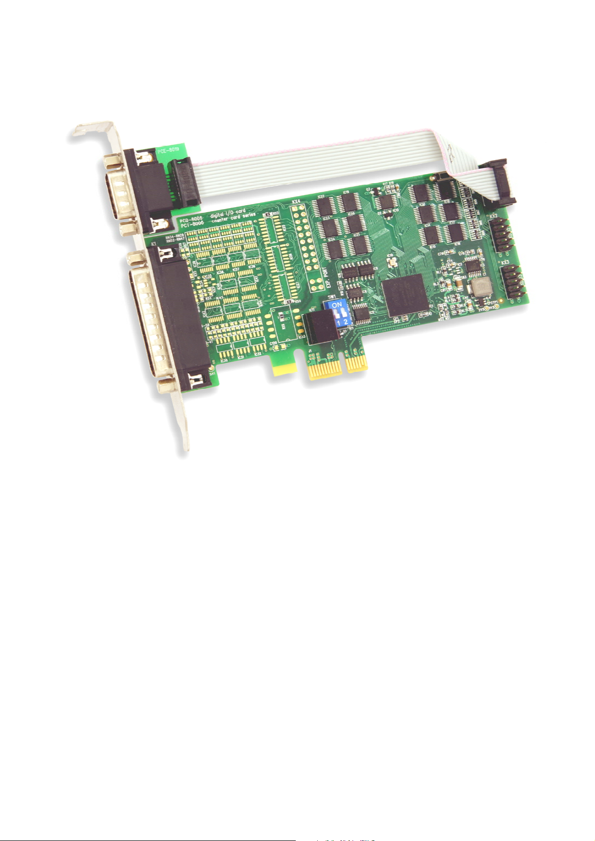
The PCD-8006 is add-on PCI Express card intended especially for laboratory and industrial
automation and measuring systems.
The PCD-8006 card provides especially these features:
• six 8-bit bidirectional digital ports, software configurable as input or output
• IRQ logic with interrupt sources derived from rising or falling edge of each digital port
signal (i.e. 96 individually programmable interrupt sources) and internal timer
The PCD-8006 card is available in two versions:
PCD-8006 standard format card
PCD-8006/LP low-profile format card
In the following text, unless otherwise stated, the designation PCD-8006 applies to both
versions of card.
1.2 General instructions for use
The PCD-8006 card is suitable for installation in either office or industrial computers that are
fitted with the PCI Express bus (Gen 1 compatible).
Cable types and their maximum length are described in paragraph 2.3 General data.
Caution:
The cards are designed for DAQ&C applications and may be used only according to the
manufacturer's recommendations and precautions given in this manual and other general
standards and terms and may be used only such a way, that its failure caused by any reason
will not be dangerous to any person or property.
1.3 Note on the contents of the manual
This manual contains all information related to card features, I/O connectors etc., but does
not include a description of installing and using drivers.
For information about drivers and programming check the dedicated documentation.
1.4 New firmware versions and customer´s firmware
The PCD-8006 card is based on a FPGA unified core providing implementation of PCI
Express bus and all peripheral circuitry, e.g. solution that gives maximum control and
supervision over full functionality. High concentration of control algorithms within FPGA
allows to add or modify functions without redesign the board (e.g. firmware with added
special custom features or a build completely new custom firmware).
A simple software utility for user-friendly firmware upgrade is available.
1. Introduction
PCD-8006 User Guide
rev. 10.2015 I - 1

2.1 Digital ports
Number of ports: six 8-bit bidirectional ports
Operating levels: HC/HCT/TTL
Load impedance of outputs: 500 Ohm min.
Note: Digital bidirectional ports are not protected against overvoltage, stresses outside the
range 0÷5 V will may cause permanent damage.
The digital ports in the output mode are durable to permanent short-circuit against
GND while maintaining the maximum current of the 5V power source (see
paragraph 2.3 General data).
2.2 Interrupt logic
Interrupt sources: timestamp IRQ generator (1÷255 ms),
all digital ports
Interrupt trigger event: timestamp generator overflow,
any combination of rising or falling edges on all
digital ports
2.3 General data
Bus type: PCI Express (x1, Gen 1)
PCI ID: VID=1760H, DID=0800H
Bus power consumption: 300 mA typ. @ 3.3 V (500 mA max.)
150 mA typ. @ 12 V (500 mA max.)
Internal power supply: 1A max. @ 5 V (see note below)
Board dimensions:: 56 x 128 mm approx. (PCE-8019 not included)
Connectors: D-Sub 25 - male (DIO ports 0, 1 a 2)
10 pin header type (DIO ports 3, 4 a 5)
Operating temperature: 0÷60 °C
Storage temperature: -20÷70 °C
Operating humidity: 10÷90 %, noncondensing
Recommended cable length: shielded cables, 2 m max.
Note: The internal 5V power supply voltage is generated by the on-board circuits from the
12V PCI Express bus power source and is used to supply the DIO ports and also to
supply PCE-16xx series external boards (see description of KX1÷KX3 connectors).
The total current of all 48 DIO signals when output mode is selected, including the
current consumption of PCE-16xx boards, must not exceed the permitted value.
2. Specifications
PCD-8006 User Guide
rev. 10.2015 I - 2

3.1 Introduction
Attention has been focused on achieving a high quality and reliability during the
manufacturing process and attention was also paid to an inspection of the card before
being shipped to you. Detailed reading of this guide and following the instructions
precisely are highly recommended for achieving full quality and to prevent any damage
during installation. For further information see manufacturer's website http://www.tedia.eu.
3.2 Hardware configuration
The PCD-8006 card contains a single configuration element - a two-segment DIP switch (the
status of this switch can be read by the program to identify multiple cards as CardID value).
Check Figure 1 in Appendix of this manual for more information.
3.3 Installation
Important Warning:
While installing the card, please follow the principles for handling the circuits, which are
sensitive to the electrostatic discharge damage. Touch the card carefully only by the edges,
and do not touch the components or metal contacts on the bottom of the card.
The computer must be switched off before the card is installed. Always disconnect the
power supply cord and other cables connected to the PC!
The cards may be stored only in an antistatic wrapper outside of the computer. Failure to
comply with the rules listed above may lead to damage of the sensitive circuits of the card,
or even of the whole computer.
After removing the slot cover plate, plug the configured card into a free slot for expansion
PC cards and fix it in place.
If you plan to use the digital ports DIO4 and DIO5 of standard format card, install the
PCE-16xx series board (not included in the delivery package of the card) into the next
position and connect the flat cables. Similarly, if you plan to use the digital ports DIO3,
DIO4 and DIO5 of low-profile card, install the PCE-8025/LP adaptor board (not included in
the delivery package) into the next position and connect the flat cables.
Note: In the event of any queries, please contact the manufacturer's technical support.
See http://www.tedia.eu for more contact information.
3.4 Location of switches and connectors
See the Appendix, Figure 1 for location of configuration switches and connectors.
3.5 Connector pin assignment
The connector pin layouts are shown in Table 1 through Table 3, the connector pin
assignment is shown in Figure 2 (all in Appendix of this manual).
3. Installation
PCD-8006 User Guide
rev. 10.2015 I - 3

4.1 Introduction
The PCD-8006 card provides six 8-bit bidirectional digital ports.
The first three ports (identified as DIO0, DIO1 and DIO2) use the D-Sub 25 connector
located on the card bracket, the other three ports (ie. DIO3, DIO4 and DIO5) use header
type connectors located at the back edge of the card.
In case of the standard format card (ie. PCD-8006), the DIO3 port is accessed on the card
bracket via adapter cable PCE-8019 terminated with D-Sub 9 connector. Remaining two
ports (ie. DIO4 and DIO5) can be accessed via adapter cable PCE-1620 (card bracket with
D-Sub 9 connector), or other types from the PCE-16xx series adapter boards.
Note: Unlike the adapter cable PCE-8019, the PCE-16xx boards are not included in the
delivery package of the card.
In case of the low-profile format card (ie. PCD-8006/LP) all three ports DIO3, DIO4 and
DIO5 can be accessed via adapter cable PCE-8025/LP (low-profile card bracket with D-Sub
25 connector); there are currently no other option available.
Note: The PCE-8025/LP adaptor board is not included in the delivery package of the card.
The signal direction of DIO port (ie. input or output option) can be selected independ for
each 8-bit port (it is not possible to select direction individually for each of the eight signals
of one DIO port) from the user software.
The port direction and output data after computer is turned on or restarted are stored in the
on-board EEPROM memory and can modify by the software utility (by default, all ports are
set as input).
4.2 Description of digital ports
Drivers and receivers based on HCTMOS technology were used for digital ports.
In the output mode (ie. driver mode), the HCTMOS circuits provide true 5 V signal levels
with a high output current with low voltage drop and can therefore be used for direct
control of LEDs, optocouplers, or miniature relays (coil parameters 5 V, 500 Ohm).
In the input mode (ie. receiver mode), the HCTMOS circuits provide not only TTL signal
compatibility, but moreover high input impedance, very low leakage current and
protection diodes. The unconnected state of inputs represents the H logic level generated
by pull-up resistors 10 kOhm against a voltage of 5 V, and the inputs can be therefore also
used to direct connecting of floating contacts.
Check the Appendix, Figure 3 for detail information.
Note: Unfortunately, the concept of bidirectional ports does not provide the overvoltage
protection available to other ports of PCI/PCIe TEDIA cards.
4.3 Interrupt logic
The PCD-8006 card allows to trigger an interrupt (simultaneously with the timestamp IRQ
generator) by any combination of rising or falling edges of the signals of all digital ports.
4. Digital Ports
PCD-8006 User Guide
rev. 10.2015 I - 4

Figure 1. Location of switches and connectors on both version of card.
K1 connector of digital ports DIO0÷DIO2, ie. DIO00÷DIO23 signals (D-Sub 25 - male)
KX1 connector of digital port DIO3, ie. DIO24÷31 signals (2x5 pin header type)
KX2 connector of digital port DIO4, ie. DIO32÷39 signals (2x5 pin header type)
KX3 connector of digital port DIO5, ie. DIO40÷47 signals (2x5 pin header type)
SW1 DIP switch for identifying multiple cards (CardID value)
PCE-8019 adapter cable PCE-8019 terminated with D-Sub 9 male connector
(included in the delivery package of the standard format card)
KE1 button for activating backup firmware (intended for service purposes)
PCD-8006 User guide - Appendix, Tables and Figures
rev. 10.2015 II - 1
Ser.No.PCD-8006
PCE-8019
PCD-8006
Ser.No.PCD-8006
PCD-8006/LP
K1
KX1
SW1 1 2
ON
ON ON
ON
OFF
OFF
OFF OFF
ID=0
S1 S2
ID=1
ID=2
ID=3
KX2
Card ID
KX3
KX1
SW1 1 2
ON
ON ON
ON
OFF
OFF
OFF OFF
ID=0
S1 S2
ID=1
ID=2
ID=3
KX2
Card ID
KX3
K1
KE1
K1 signal (PCE-8025/LP) pin pin K1 signal (PCE-8025/LP)
DIO0 (DIO24) C1 C14 DIO1 (DIO25)
DIO2 (DIO26) C2 C15 DIO3 (DIO27)
DIO4 (DIO28) C3 C16 DIO5 (DIO29)
DIO6 (DIO30) C4 C17 DIO7 (DIO31)
DIO8 (DIO32) C5 C18 DIO9 (DIO33)
DIO10 (DIO34) C6 C19 DIO11 (DIO35)
DIO12 (DIO36) C7 C20 DIO13 (DIO37)
DIO14 (DIO38) C8 C21 DIO15 (DIO39)
DIO16 (DIO40) C9 C22 DIO17 (DIO41)
DIO18 (DIO42) C10 C23 DIO19 (DIO43)
DIO20 (DIO44) C11 C24 DIO21 (DIO45)
DIO22 (DIO46) C12 C25 DIO23 (DIO47)
GND C13
Table 1. D-Sub 25 (male) connector pin assignment.
Note: The signal names before the bracket apply to the connector K1 located on card, the
signal names in brackets apply to the connector located on PCE-8025/LP adapter.
KX1/KX2/KX3 signal pin pin KX1/KX2/KX3 signal
DIO24/32/40 D1 D2 DIO25/33/41
DIO26/34/42 D3 D4 DIO27/35/43
DIO28/36/44 D5 D6 DIO29/37/45
DIO30/38/46 D7 D8 DIO31/39/47
GND D9 D10 5V (see specification chapter)
Table 2. Header type connector pin assignment.
Note: In case of the standard format card, the DIO3 port is accessible on the card bracket
via adapter cable PCE-8019 terminated with D-Sub 9 connector. Remaining two ports
(ie. DIO4 and DIO5) can be accessed via adapter cable PCE-1620 (card bracket with
D-Sub 9 connector), or other types from the PCE-16xx series adapter boards.
In case of the low-profile format card all three ports DIO3, DIO4 and DIO5 can be
accessed via adapter cable PCE-8025/LP (see Table 1).
signal pin pin signal
DIO24/32/40 C1 C6 DIO25/33/41
DIO26/34/42 C2 C7 DIO27/35/43
DIO28/36/44 C3 C8 DIO29/37/45
DIO30/38/46 C4 C9 DIO31/39/47
GND C5
Table 3. D-Sub 9 (male) connector pin assignment located on PCE-8019 (single
DIO port adapter cable) and PCE-1620 (dual DIO port adapter cable).
PCD-8006 User guide - Appendix, Tables and Figures
rev. 10.2015 II - 2

Figure 2. Pin layout on D-Sub 25 (male), D-Sub 9 (male) and header type connectors
(2x 5 pins, 2.54 mm pitch).
Figure 3. Simplified schematic of DIO ports.
The diagram shows one bidirectional I/O channel.
The signal direction of DIO port (ie. input or output option) can be selected independ for
each 8-bit port, but it is not possible to select direction individually for each of the eight
signals of one DIO port.
PCD-8006 User guide - Appendix, Tables and Figures
rev. 10.2015 II - 3
5
4
3
2
1
6
7
8
9
10
11
12
13
14
15
16
17
18
19
20
21
22
23
24
25
8
7
6
5
4
3
2
1
9
12
910
3
5
7
4
6
8
10K
GND
+5V
TTL
DIOxx 33R
DIO port mode
=> INPUT
ON
OFF
=> OUTPUT
INPUT mode of DIO port
>500R
OUTPUT mode of DIO port
data
DIN
data
DOUT
PCIe card
DIOxx
DIOxx
GND
GND
HCT
HC

.............................................................................................................................
.............................................................................................................................
.............................................................................................................................
.............................................................................................................................
.............................................................................................................................
.............................................................................................................................
.............................................................................................................................
.............................................................................................................................
.............................................................................................................................
.............................................................................................................................
.............................................................................................................................
.............................................................................................................................
.............................................................................................................................
.............................................................................................................................
.............................................................................................................................
.............................................................................................................................
.............................................................................................................................
.............................................................................................................................
.............................................................................................................................
.............................................................................................................................
.............................................................................................................................
.............................................................................................................................
.............................................................................................................................
.............................................................................................................................
.............................................................................................................................
.............................................................................................................................
.............................................................................................................................
.............................................................................................................................
.............................................................................................................................
.............................................................................................................................
.............................................................................................................................
PCD-8006 User Guide - Notes


Table of contents
Other TEDIA PCI Card manuals


