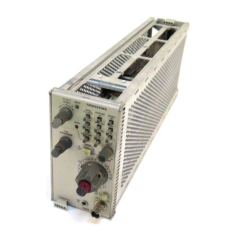
Tektronix 5B42 User manual

TEKTRONIX®
1-
DELAYING TIME BASE
INSTRUCTION MANUAL
Tektronix, Inc.
P.O. Box 500
Beaverton, Oregon 97005 Serial Number
070-1447-00 373

5B42
SECTION 1
SECTION 2
SECTION 3
OPERATING INSTRUCTIONS
Instrument Description
Preparation For Use
Basic Operation
Triggered Display
Single Sweep Mode
Dual Trace Display Switching
Delayed Sweep
Triggered Delay Sweep
External Horizontal Amplifier
Specifications
THEORY OF OPERATION
Introduction
External Horizontal Amplifier
External Trigger Channel Switch
Internal Trigger Channel Switching
Main Trigger Comparator
Delayed Trigger Comparator
Main Trigger Generator
Delayed Trigger Generator
Sweep Control
Main Sweep Generator
Delayed Sweep Generator
Output Suffer
Readout
Timing Switch Details
SERVICE INFORMATION
Services Available
Maintenance
Repackaging for Shipment
Symbols and Reference Designators
Electrical Parts List
TABLE
OF CONTENTS
Page
1-1
1-1
1-2
1-2
1-2
1-2
1-2
1-2
1-3
1
-
4
21
2
-
1
2-1
21
2-1
21
2-1
22
2-2
2-2
2-2
23
2-3
2
-
3
3
-
1
3-1
3-1
3-2
3-3
Internal Adjustment Procedure
Parts Location Grid BBoard {SN B053592 &Bel owl
Controls, Connectors &Block Diagram
Parts Location Grid ABoard (SN RQ59999 &Below]
External Trigger Channel Switching Schematic
Parts Location Grid BBoard (SN B053592 8t Up
l
Internal Trigger Channel Switching Schematic
Parts Location Grid ABoard (SN B06QDQD St Up)
Main Trig Gen (SN B060000 &Up],
Dlyd Trig Gen (SN B053593 &Up)
Main Trig Gen <SN B059999 &Below).
Dlyd Trig Gen (SN B0G3592 &Below)
Sweep Control &Main Sweep Generator Schematic
Delayed Sweep Generator Schematic
Readout Switching Schematic
Timing Switch Details Schematic
Mechanical Parts List
Exploded View
Accessories
REV, C, AFR. 1978 1

iflft’ter
MSlYIVfc
«i«f eRM-TlWi
;j** w-Bfes^*
imm?,
amxvai
"t w- :'r
jw>*. _.“J '«
affr-w;
manii i
’MSJVfct
Stjy'Htt; ::
r?miW«*tf bB4?: «fet.AVJ»G n«£ SA$£
©
5B 4-2

Section 1-5B42
INSTRUMENT
The 5B42 Delaying Time; Base provides normal and fully
triggerable delayed sweeps tor the 5400 series oscilloscopes.
It features edge-lighted main and delayed SEC/DfV selector
switches. When used In amainframe with readout capa-
bilities, the SEC/DIV information is displayed on the CRT
face. AH front panel controls are conveniently grouped and
OPERATING
INSTRUCTIONS
DESCRIPTION
color coded for ease of identification end operation.
Pushbuttons select various trigger modes from either
vertical plug-in compartment and the various sweep modes.
Although designed for use in the right hand or sweep
compartment of the oscilloscope, the 5B42 will operate in
the vertical compartments to produce vertical sweeps.
PREPARATION FOR USE
Your 5B42 is calibrated and ready for use when
received. Fig. Ifshows installation-removal procedure,
Refer to the Front Panel Controls illustration in the fold-
out pages for acomplete description of the front panel.
Color patterns, printed on the front panel help to identify
functionally grouped controls. Blue surrounds controls
associated with the display mode, light green with the main
trigger, and dark green with the delayed trigger controls.
Also, the shades of grey on the TRIG LEVEL controls
correspond with the grey on the SEC/DIV switch knobs tor-
easy Identification.
Fig. 1-1. EB42 Insta Mat ion-R umova [Procsdure.

Operating instructions-5B42
BASIC OPERATION
NOTE
Effective SN BD90000 and up, the MAfN SEC/Df V-DL Y'D SEC/DiV knob assembly is manufactured with
alocking pin removed from the assembly (all instruments below SN B090000 use alocking pinf. This pin
removal allows the Delayed Sweep to operate at aslower sweep rate than the Main Sweep rate. Avoid this
type of operation to prevent illogical displays, arid always set the DL Y'D SEC/DIV control for the same or
afaster sweep rate than the MAIN SEC/DiV control.
Triggered Display
With the 5B42 Time Base properly installed in the
horizontal plug-in compartment, apply power to the main
frame. Connect the CALIBRATOR output on the display
module to the vertical plug-in. Adjust die vertical plug-in
gain for atwo division display. Push the LEFT or RIGHT
TRIGGER SOURCE button, depending on which compart-
ment contains the vertical plug-in. Push the MAIN SWEEP
button in the MODE column, and the AUTO TR IG button
in the light green TRIG SOURCE area. Rotate The position
controls for the vertical plug-in and 5B42 until atrace is
visible, Adjust the MAIN TRIG LEVEL control until the
display stabilizes. Now rotate the MAIN TRIG LEVEL
control from stop to stop. Notice that the trace free runs
over most of the control rotation. Release the AUTO TRIG
button and rotate the MAIN TRIG LEVEL control from
stop to stop. Notice that the trace appears only when It is
triggered, and disappears over most of the control rotation.
Single Sweep Made
Obtain astable display, positioning the sweep so that the
start is visible. The sweep is starting on the negative-going
portion of the square wave. Push the +SLOPE button. The
trace will start on apositive-going waveform. Remove the
jumper front the calibrator to the vertical plug-in. Depress
the button labeled SlNGL SWP. The READY light is now
visible. Watch the CRT, and touch the jumper to the
vertical plug-in input. If the intensity is high enough, afast
single trace will be visible and the READY light will
extinguish, Remove the signal to the vertical, and depress
the RESET button. The READY light will be visible again,
arid the sweep i$ rearmed. Release the SINGL SWP button
and obtain astable display by pushing the AUTO TRIG
button, and adjusting the MAIN TR IG LEVEL control.
Dual Trace Display Switching
The button labeled CHOP in the blue DISPLAY MODE
section of the front panel selects the switching mode for
dual sweep vertical plug-ins. With the button out, the
switching is done in the alternate mode, i.e., one channel is
displayed for one full sweep, and then the other channel is
displayed. This can be demonstrated by using aduai
channel vertical plug-in and slowing the 5B42 sweep speed
to about 10 nns/div with the truce free running. Pushing the
button in gives the chopped mode.
Use the chopped mode for viewing slower dual -trace
displays and the alternate mode for faster displays. Return
the vertical plug-in to a single channel display and re-
connect the calibrator waveform.
Delayed Sweep
Set the DELAY TIME MULT dial to mid-range. Obtain a
triggered display. Push the IIMTENS SWP button in the blue
DISPLAY MODE column. Notice the number illuminated
in the outer ring of the SEC/DIV sweep dial. Set the
DLY'D SEC/DIV to 1mand the MAIN SEC/DIV to 5m.
Reduce the INTENSITY control on the display module
until aportion of the display is visible as an intensified
portion. Rotate the DELAY TIME MULT dial and notice
the brightened portion move smoothly across the display.
The brightened portion represents the delayed sweep, and
occurs in one fifth the time of the main sweep according to
the described SEC/DIV switch settings. The delayed sweep
speed is independent of the main sweep speed, and may be
set to any speed equal to or faster than the main sweep.
Press the DLY'D SWP pushbutton In the blue DISPLAY
MODE column; the bright portion of the display will spread
across the entire CRT. See Fig. 1-2 A.
Triggered Delayed Sweep
Press the TRIG AFTER DLY and the INTENS SWP
pushbuttons and adjust the DLY’D TRIG LEVEL control
for astable display with an intensified portion. Rotate the
DELAY TIME MULT dial and the brightened portion will
jump from waveform to waveform. Push the -i SLOPE
button located in the dark green area above the DELAYED
TRIG LEVEL knob. The start of the intensified portion
will shift from the negative portion of the waveform to the
positive portion. Press the DLY'D SWP pushbutton. The
intensified portion of the triggered waveform is now
displayed across the entire CRT, Return to the INTENS
SWP mode. In this mode the delayed sweep will not start
until the main sweep has passed the number of divisions
shown on the DELAY TIME MULT dial. The next trigger
after this point will start the delayed sweep. One purpose of
the triggered mode is to eliminate jitter that may be present
in highly magnified displays. Another purpose is to select
the trigger starting the delayed sweep. For example, to view
alow level signal impressed on ahigh level signal, trigger the
main sweep on the high level signal and the delayed sweep
1-2 REV BJJN 1979

Operating lnstructmns-5B42
fIntensified port ion
fof Waveform
{
\\V
I
{
\\
II II "" "J0
r'
!
.
:Delayed sweep display
Delsy time
-Main sweep time
Mein trigger
pulse
Main sweep
"arms" delayed -sweep
Delayed sweep waits
for next trigger
i—
—
Delayed trigger poise
X- Bsweep time
—
I
F
i;
?rf
mrF
F~i
'Main sweep display
-V-—j- —-j
iIntensified portion \
)of waveform V
f\
<——,4-
1
1i
\
\
!/
i
S\
\\
~i\—
J/ *
'i i-n*
i
r
u:0alayed sweep display
[A| Delayed sweep starts after delay time. fB) Delayed sweep triggered after delay time.
Fig. 1-2. Relationships of Main and Delayed sweeps.
on the low level signal. Select the portion to trigger the
delayed sweep in the intensified mode- See Fig. 1-2B
Press the SWP MAG billion and notice the sweep speed
increase by tin order of magnitude. This is shown on the
SEC/D IV dial and the CRT readout.
|f the waveform viewed is line -frequency related, push
the button labeled LINE in the light green TRIG SOURCE
column. The signal activating the trigger circuits in this
mode is taken from the power line. External triggers may
be. applied 'to the EXT TRIG connector. Push the button
labeled EX Tin the light green TRIG SOURCE column.
External Horizontal Amplifier
To use the 5B42 as an amplifier, rotate the MAIN
SEC/DIV switch fully CCW to the AMP position. Apply the
calibrator waveform to the BMC connector marked EXT
HORIZ AMPL. Two dots approximately eight divisions
apart are visible. There is no front-panel gain adjustment for
the external horizontal amplifier.

Operating Instructions— 5B42 SPECIFICATIONS
All references to divisions or VOLTS,'DIV refer to major graticule divisions in this manual.
Main Sweep SINGLE SWEEP; Same requirements as main sweep.
ACCURACY: (Measured in 5400 series oscillo-
scope over center 8graticule djvi
sions. Exclude the first 30 ns and
the last 10 div ot the magnified
sweep)
:
-i-1 5'JCto 0'~ Cto T5CiuC
Unmag Mag Unmag Mag
1s/div to 05^s/rliv 3% 4% 4% 5.5%
5 s/div and 2s/div
0.2 ps/div and
0.1 p-s/div
4% b% 5% 6.5%
Any two divisions
within center 8
divisions
6.5% 6.5% 3% 8%
VARIABLE RANGE: Continuously variable between cali-
brated sweep rates. Extends sweep
rate to at least 12.5 s/div.
TRIGGERING:
Coupling
Vertical
Plug 1n
Series
Freq,
Range
Minimum
Signal
Required
1nt. Ext.
DC 5400 DC to
10 MHz 0.4 div 100 mV
10 MHz to
60 MHz 1.0 div 400 mV
5100 DC to
2MHz 0.4 div
AC Req uirements
increase bdow
50 Hz.
LF REJ Requ irements
increase below
f.b kHz.
TRIGGER LEVEL >+8div.
RANGE:
EXTERNAL TRIGGER
INPUT:
Maximum input 350 VDC ipeak AC, 350 VP-P
voltage: AC at <1 kHz.
nput Rand C: 1MO ±2% paralleled by ~20 pF.
Trigger LeveI2.5V.
Range
Delayed Sweep
ACCURACY: (Measured in 5400 scries oscillo-
scope over center 8graticule divi-
sions) :
-M5°C to t35°C 0°C to -t-50°C
Unmay Mag LJ nmug Mag
0.1 s/div to
0.5 p's/d iv
3% 4% 4% 5,5%
0,5 s/div and
0.2 s/div; 0.2 psf
div and 0.1 AE/d5v
4%. 5'% 5% 6.5%
Any two divisions
within center S
divisions
6.5% 6.5% 8%
TRIGGERING:
DC to 10 MHz:
60 MHz:
EXTERNAL HORI-
ZONTAL INPUT:
Deflection Factor:
Bandwidth.
DC Coupled
:
AC Coupled
:
0.4 div.
1div.
50 mV/div ±3%.
DC to >2 MHz.
<50 Hz to >2 MHz
1-4 REV. FEB 1974

Operating fnstructions-5B42
Delaying Sweep Characteristics
DELAY TIME MUL- 0,2 to IQ tii
TIPLIER RANGE; setting.
INHERENT DELAY <100 ns.
TO START OF
DELAYED SWEEP;
DIFFERENTIAL TIME
MEASUREMENT
the TIM E/D IV ACCURACY;
1jua/div to 0.5 s/div delay <1 %+0.2% of full scale,
time:
1s/div to 5s/div delay <2% h0.2% of full scale,
time;
JITTER: <1 part in 20,000 of TO times
the main TIME/D IV setting.
Rev. FEB 1974 1-5

Section 2-5B42
THEORY
OF OPERATION
Introduction
Refer to the complete schematic diagrams, and the block
diagram, located in the pullout pages at the back of this
manual, for acomplete understanding of the 5B42 theory
of operation.
External Horizontal Amplifier
Signals applied to the EXT HORIZ AMPL input, JTO,
are fed through adivide-by-two attenuator, consisting of
R11,R15, and AC compensating capacitor. Cl 5, to the
gate of source follower Q20, When $10A is in the AC
COUPL position, Cn AC couples the signal to Q2Q. The
circuit DC balance is set by R25 through G24. In the AMP
mode, the signal, travels past protective diodes CR30 and
VR30 to Q34, an emitter follower. The emitter of Q34
drives the emitter of Q36, operating as an operational
amplifier. Tha feedback path is through VR42, R45rR50,
and R52. The latter sets the gain at two. The amplifier is
disabled, when the MAIN SEC/DIV switch is not in the
AMP position, by raising the common emitters to about
-1-5 V. The output from the amplifier is the junction of
VR42 end R45. Positioning in the external mode is
accomplished by asuction of the main POSITION control
connected to the base of Q36 through R49.
External Trigger Channel Switch
The purpose of the trigger switches is to isolate the
unwanted trigger source. They also provide gain. The
output of Q20 feeds the base of G6Q, whose emitter drives
Q62 in agrounded-base configuration. The output of Q62
drives Q8Q as agrounded base amplifier. The base level of
QttO is set by CR80, R80, R83, and R85. To prevent
coupling of the trigger signal through the switch, the
emitters of Q60 and Q62 are disconnected from —15 V,
The collector of Q62 rises toward '15 Vas Q62 is turned
off. Diode CRSl conducts, and causes avery low impedance
to ground at the. output of Q62. CR81 maintains the DC
stability of the circuit, and shorts any capacity-coupled
signal that may be present on the collector of Q62 to
ground, C9o AC-couples the output of either Q80, Q90,
or Q23Q in the AC-coupled mode. C99 and R280 form a
high pass RC combination for rejection of low frequency
signals. Q9QT base is connected to asecondary of the line
transformer. Alow level voltage at line frequency is
obtained for tine triggering. G60rQ62fQ20G, and 0210
are disabled in the line mode by removing the —15 Vfrom
their emitters.
Internal Trigger Channel Switching
These switches {Schematic 2) operate in the same
manner as The switch described in the preceding paragraph.
The trigger signal from the right vertical plug-in is applied
to the base of Of 00, through pin 4A on the rear interface
connector. The left vertical plug-in trigger signal is applied
Through pin 4B to the base of Q15D. The outputs of the
right or left trigger switches are applied to the internal
trigger channel switch, and then to the main trigger
comparator (Schematic 3). CR235 holds the base of Q23Q
positive when the plug-in is operating in the external
amplifier mode to prevent coupling of any trigger signals
from either vertical plug-in to the external horizontal
amplifier.
Main Trigger Comparator
This circuit selects the voltage level on the waveform
where triggering takes place. The triggering signal is applied
to the base of Q2B0, Q280 and Q2-90 serve as avoltage
comparator, The DC level at the base of Q290 is set by
R320, the MAIN TRIG LEVEL control. If the voltage at
the base of G2S0 is higher, current will flow through Q280
and the collector of Q290 will be high. The opposite is true
if the base voltage of Q2S0 is lower, and the- collector of
Q290 will be low. C285 and R285 improve high frequency
response. LR293, C293, LR299, and C299 prevent
coupling of switching transients into the voltage supply
lines.
Delayed Trigger Comparator
This comparator operates in the same manner as the
Main Trigger Comparator. The input to the base of 0370 is
selected from either the right or left trigger channel switch.
It is not possible to trigger the delayed sweep externally.
Main Trigger Generator {SN B059999 and below)
This circuitry uses emitter-coupled logic. Significant
high levels arc approximately 4.2 V, and low levels 3.2 V,
Low amplitude analog trigger signals may operate gates
U32Q, U330A, U330B, and U335A. The remainder of the
gates operate at digital levels exclusively.
Input to the main trigger generator is pin 7 of U320,
an exclusive OR gate. Pushing the -+ SLOPE button sets
alow on pin 9, which allows U320 to operate as a
rion-iri verting amplifier with again of five. Apositive-
REV, CJUN 1977 2-1

Theory of Operation—5B42
going trigger signal at pin 10 of U320 causes apositive
output from pin 14 of U335C which starts the sweep.
U335B and Cform alatch, which generates the sweep gate.
When the sweep ends, the junction of R356 and R357 goes
high, setting latch U330C and Dso that ahigh is on pin 14
of U330C, This high resets latch U335B and C. In this state,
U335C can not initiate asweep gate. When the holdoff
time passes, the junction of R356 and R357 goes low, A
low at pin 6of U33Q8, or the next negative-going trigger,
causes letch U330C and Dto reset, enabling latch U335B
and C. The next 'positive Output from U320 initiates the
sweep gate by lowering pin 13 of U335C. When negative
slope Triggering is desired, ahigh is placed on pin 9of
U32C, which allows U320 to operate as an inverting
amplifier with again of five.
Main Trigger Generator (SN B060000 and up)
Integrated circuit U300 converts the trigger comparator
output signal to agate that is used for sweep control. With
pin 1connected to ground l+SLOPE), apositive-going
signal on the input (pin 13} causes the output (pin 3) to
rise to about 4.1 V. Pin 14 is negative-going under these
conditions. The output, gate occurs when aTrigger signal
passes through the hysteresis limits at the input of U300
(pin 13 rs within 20 mV of pin 14). Placing pin 1at +5 V
(—SLOPE) creates an output gate at pin 3, when pin 13 is
negative-going and pin 14 positive-going. After completion
of the sweep, and during holdoff Time, pins 6and 10 are
high [about +4.2 V), This action inhibits the trigger gener-
ator until these pins drop to about +3.2 V, which occurs
after completion of holdoff time.
Delayed Trigger Generator (SN B059999 and below)
This generator operates, in the triggered mode, in the
same manner as the main trigger generator. In the delayed
sweep and intensified sweep modes, the delayed sweep
starts when the junction of R438 and R44Q goes low. The
highs placed on pins 14 and 15 of U410, through diodes
CR4T0 and CR411, cause acontinuous low at pin 6of
U420E3. This causes pin 12 of U425C to go low at the
beginning of the delayed pickoff gate. Pin 9of U425B is
held high, causing acontinuous low on pin 13 of U426C.
Two lows at the inputs of U425C cause ahigh at pin 14
starting the delayed sweep runup.
Delayed Trigger Generator (SN B060000 and up)
Inthe Trig After Delay mode, this generator operates in
the same manner as the Main Trigger Generator, U300. The
delayed sweep starts when two conditions are met; the
delay gate at pin Gand 10 of U40Q must be low (approxi-
mately +3.2 V), and atrigger signal must pass through the
hysteresis limits at the input of U400 (i.e., pin 13 is within
20 mV of pin 14).
Sweep Control
U450, with additional external circuitry, controls the
main sweep generator. In the automatic triggering mode,
pin 19 of U450 is connected to ground. If pin 1of U450
receives no trigger pulses from the main trigger generator
for aperiod of time determined by R495 and C495,
circuitry in U450 outputs anegative-going square wave.
This negative-going square, wave from pin 3of U450, drives
the base of Q430 negative. The collector goes positive and
stays positive for the duration of the sweep. Apositive
pulse at the emitter of Q480, from the trigger switches, also
causes the collector of 0480 to go positive, starting the
sweep. This positive pulse is also applied to the unblanking
circuitry, in the plug-in and the mainframe, to unblank the
CRT during the sweep.
The sweep ramp is fed to the base of Q470, which forms
acomparator with Q460, Q470 is conducting and Q460 is
off. As the ramp rises, current flow in Q470 is reduced until
CR460 is forward biased, and Q460 comes sharply into
conduction. This positive pulse at pin 16 of U45Q causes
the auto gate (from pin 3) to go positive, terminating the
sweep through Q4S0. If the unit is operating in the
triggered mode, apositive gate appears at pin 17, lowering
the sweep gate via the main trigger generator and G480,
terminating the sweep}
As the sweep ramp decays toward ground, Q460 and
Q470 switch, so that pin 16 of U450 again goes low. No
negative pulse can appear at pin 3 to start the next sweep.
Pin 17 remains high, locking out the main trigger generator
until holdoff time is completed. This time is determined by
C50C, R50G, 0501 and CB02. These components are
switched according to sweep rates, as shown in the switch
details. Holdoff is necessary to allow all sweep -generating
circuits to discharge before the start of the next sweep.
When the external horizontal amplifier mode is used, pin
18 of U45Q is connected through CR455 to +5 V. This
disables the sweep until the switch is opened.
In the single sweep mode, the automatic trigger capa-
bility is removed by ungrounding pin 19 of U450. Pin 12 is
connected to +5 V, The next trigger operates the sweep in
the normal manner. The gate at pin 17, however, remains
high, locking out further triggers until pin 11 of U450 is
grounded and pin 15 is connected to +5 Vthrough the
spring-loaded RESET button. VR49Q and CR490 provide
-5 Vfor U450.
Main Sweep Generator
The sweep ramp is generated in U550. The ramp is fed
to the horizontal amplifiers and the sweep control from pin
8. Timing capacitors Ctand timing resistors Rtdetermine
the rate of rise. The DELAY TIME MULT potentiometer
2-2 REV. B, JUNE, 1977
Theory of Operation—5B42
controls one half of acomparator in U550. The other half
is connected internally to the ramp. Whan the ramp voltage
reaches the voltage on the center arm of the delay time
potentiometer, pin 4of U55Q goes high, driving the
collector of Q570 low. This low gate starts the delayed
sweep through the delayed trigger generator. Alow at the
collector of Q574 deactivates the delayed sweep by locking
pin 4of U550 in the low state. This occurs only when
operating in the main sweep mode. When operating In other
than the main sweep mode, pin 5of U550 is high during
main sweep time, allowing the delayed sweep to start at the
selected time G540aids in reducing sweep jitter, and R545
compensates for leakage current in U550.
Delayed Sweep Generator
The delayed sweep generator integrated circuit is identi
cal to the one used in the main sweep. Several external
connections are changed to suit the delayed sweep opera-
ting inode. Pin &of U600 is always connected to +5 V,
enabling the generator whenever the plug-in has power
applied. When the positive sweep gate from the delayed
trigger generator is applied to pin 1, the sweep starts, and
the CRT is unblanked through the emitter of Q69G. The
sweep runs up until the delayed trigger generator receives a
positive-going pulse from Q570. The delayed sweep gate, at
pin 1of U600, goes negative, the CRT is blanked and the
sweep decays. If die sweep lime of the delayed sweep is
much taster than the main sweep, the delayed svireep ramp
will reach 10 V, its Urn It, before the gste at pin 1returns
the ramp to ground. The voltage at pin 8is fixed at 10 V.
As the ramp rises past 10 V(at the end of the sweep) pin 4
goes high, blanking the CRT through Q690. Under this
condition, the CRT is blanked through the base of Q690
from pin 4of LIBOO, and the delayed sweep remains high
until turned off by the delayed sweep gate.
Output Buffer
Main or delayed sweep ramps are applied to the base of
0650- 0650 and QG70 comprise an emitter-coupled para-
phase buffer for ihe sweep ramp. In the magnified mode,
emitter degeneration is reduced, resulting iri an increase in
gain by ten limes. Clamping limits ihe peak to-peak
excursion at line collector of Q650 lo about 1.2 V. Q665 is
aconstant current source. Sweep positioning is accom-
plished by varying current balance in the amplifier through
the base of Q670.
When the plug-in is operated in the external amplifier
mode, the base of Q680 is connected through R632 to
+5 V. This saturates Q68G and eliminates the effect of the
position control on the base of GS70. Positioning is
accomplished in the external horizontal amplifier as
described previously. The base of 0720 is made more
positive through CR685 to unblank line CRT, Output from
the external horizontal amplifier is connected to R672, and
R672 is disconnected from ground.
The main sweep gate is applied at the base of Cl730.
CR732 conducts only whan ihe emitter of Q730 goes
negative at the end of the main sweep gate. This negative
going pulse activates circuitry in the main frame to
alternate traces in vertical plug-in's. When the CHOP
pushbutton is in, pins ISA and 20A on the interface
connector are connected together, causing the vertical
plug-ins to operate in thu chopped mode.
The main sweep gate, during sweep time, raises the base
of G720 through CR710. The collector is made more
negative and the CRT is unblanked, during sweep time,
through circuitry in the main frame. In the delayed sweep
mode, the base of Q720 is held tow, through CR712,
preventing the CRT from unblanking by the main sweep
gate, Q695 improves unblanking from the main sweep at
the faster ijweep speeds. CR6S0 and CRQ91 are protective
diodes for Q690 and the internal circuitry of U6G0
connected to pin 1.
Readout
The DLY'D, MAIN SEG/DIV,CAL, DLY'D SWP, MAIN
SWP, INTENS SWP, and MAG switches have contacts wired
into the readout circuitry, Azero to -15 Vpulse,
approximately 125 jus in length, is applied at different times
to all of the rear interface connectors associated with the
readout circuitry, except the two column and row lines.
These arc the output lines. Thu readout circuitry, in the
5842, sets the correct amount of current, to the
appropriate channel row and column lines during the pulse
time, for the particular character desired. See the main-
frame manual for more details on the time slot and current
required for each character. Connecting the anode of
CR970 to +5 V, in the AMP mode, disables both main and
delayed sweep readouts. When the DLY'D SWP pushbutton
is in, 4gV is connected to the anode of CR97T. This
disables the main sweep readout. When either the MAIN
SWP or INTENS SWP pushbuttons are depressed, the delay
sweep readout is inactivated via CR976, When the MAG
button is depressed, wo additional zeros are added to the
readout showing the correct time per division for the active
sweeps. When the CAL knob is not in its detent position,
the unca Iibrated sign O) appears in the slot for the main
sweep only. Diodes CR901 through CR933, connected to
the time slot lines, decouple noise pulses generated in the
main frame readout circuitry.
Timing Switch Details
Timing capacitors and resistors are connected according
to the switching chart shown on Schematic 7, The CAL
potentiometer varies the timing resistance in any position
of the MAIN SEC/D IV switch. Lamps DS760 through
DS76G illuminate the SEC/DlV knob skirts. The diodes in
series with the lamps prevent series current from one lamp
lighting another, in certain switch combinations.
REV. C, APR. 197S 23

Seel ion 3-5E542
Services Available Repackaging for Shipment
Tektronix, Inc, provides complete instrument repair and
adjustment at local Field Service Centers and at the Factory
Service Center. Contact your local Tektronix Field Office
or Representative for further Information.
Maintenance
Refer to the oscilloscope mainframe manual for general
service information. The "A" Board is the board on the left
when facing the front of the 5B42. The "B" Board is on the
right. To remove the Acircuit board, remove the ten
pushbuttons on the front panel located in the light green
TRIG SOURCE area by pulling straight out. Remove the
pushrods connected to the +SLOPE, SINGL SWP, and
RESET switches by separating the ends of the rods with a
screwdriver. Unsolder the white arid orange wire connected
to the POSITION control and the coaxial cable connected
to the EXT TRIG bnc connector. Loosen the 0.050 inch
Allen screw on the CAL switch shaft, accessible through
the hole in the Aboard, located as shown on the Controls,.
Connectors &Block Diagram pullout page. The knob must
be in the CAL position. Remove the shaft by pulling the
knob. Remove five screws on the ABoard and four screws
on the BBoard, as shown on the Internal Adjustment
Procedure pullout page. Fold the ABoard back to gain
access to the cam switches or other switches located
between the boards.
Removal of the BBoard will not usually be necessary,
but may be accomplished by removing all leads soldered to
the board. Remove the attached switch knobs and lovers,
and the three screws holding the board to the chassis.
If the Tektronix instrument is to be shipped to aTektronix
Service Center for service or repair, attach atag showing:
owner (with address) and the name of an individual at you
r
firm that can be contacted, complete instrument serial
number and adescription of the service required.
Save and re-use the package in which your instrument was
shipped. If die original packaging is unfit for use or not
available, repackage the instrument as follows:
1* Obtain acarton of corrugated cardboard having inside
dimensions of no less than six inches more than the
instrument dimensions; this will atEow for cushioning.
Refer to the following table for carton test strength
requirements.
2. Surround the instrument with polyethylene sheeting to
protect the finish of the instrument,
3. Cushion the instrument on all sides by tightly packing
dunnage or urethane foam between carton end instru-
ment', allowing three inches on all sides.
SHIPPING CARTON TEST STRENGTH
Gross Weight (lb) Carton Test Strength (lb)
0-10 200
10-30 275
30-120 375
120-140 500
140-100 600
Jumpers for the +5 V, +15 V, +30 V, -15 V, and -30 V
supplies are located in the lower rear comer of the ABoard.
Remove these jumpers rather than the board inter
connecting cable to isolate the ABoard from the power
supplies,
3-1REV. DMAY 1973

Service information —5B42
DIAGRAMS AND CIRCUIT BOARD ILLUSTRATIONS
Symbols and Reference Designators
Electrical Components shown on the diagrams are in the following units unless noted otherwise:
Capacitors -Values one or greater arc in picofarads (pF).
Values less than one are in microfarads (,uF).
Resistors =Ohms (O).
Graphic symbols and class designation letters are based on ANSI Standard Y32.2-1975.
Logic symbology |s based on ANSI Y32, 14-1 973 in terms of positive logic. Logic symbols depict the logic
function performed and may differ from the manufacturer's data.
The overling on asignal name indicates that the signal performs its intended function when it goes to the low state,
Abbreviations are based on ANSI Y1.1-1 972.
Other ANSI standards that are used in the preparation of diagrams by Tektronix, Inc. are:
Y14.15, 1966 Drafting Practices.
Y14.2, 1973 Line Conventions and Lettering.
Y1Q.5, 1968 Letter Symbols for Quantities Used in Electrical Science and
Electrical Engineering.
The following prefix letters are used as reference designators to identify components or assemblies on the diagrams.
AAssam b-'y. separable or repairable
(circuil board, etc}
A.i Attenuator, fixed or variable
3Motor
3T Battery
CCapacitor fixed orvariate
CB Circuit breaker
CH Diode signal or rectifier
DL Delay line
DS Indicating device (lamp)
ESpark Gap. Farrit® Peat)
FFuee
F: Filter
HR
HV
-
<
Hast dissipating tlevice (heat gink,
hem radiator, etc)
Healer
Hybrid circuit
Connector, stationary portion
Relay
Inductor, fixed &variable
Meter
Connector, movable portion
Transistor or qilicon-cortnollfid
reclifler
Resistor, fixed or variable
Therm'star
The following special symbols may appear on the.diagrams:
Strap or Lirik 1^,, P15
Cam Switch
Closure Chart
{Dot indicates
switch closure)
SEL Value Selected
at Factory
SSwitch or contactor
rTransformer
TC Thermocouple
TP Test point
UAssembly, urs&paiable or ntm-repairuble
tintegraied circuit, etc.)
VElectron tube
Vfl Voltage regulator {zener dipde, etc.)
wwirasirap or cable
VCrystal
ZPhase s-nirt&r
.Plug to E.C. Board
IBox Iidentifies Panel
.Controls, Connectors and
[BACr^ Indicators
Modified Component— See
iRIsj-'f —Parts List (Depicted in grey,
50Kor with grey outline)
Plug Index
Refer to Waveform
Fteler to Diagram Number
Assembly Number
Board Name
VERTICAL AMPLIFIHR<|>-^an
CdN
m
u
£
Coaxial Connector
Decoupled or Filtered
Voltage
Etched Circuit Board
Outlined in Black
Schematic Name
mber
3-2 REV. BMAY 1976

REPLACEABLE
ELECTRICAL PARTS
PARTS ORDERING INFORMATION
Repayment parts are available from or through your luoal Tektronix, Inc, Field Off i06
or representative.
Changes lo Tektronix instru moots art? sometimes made to accommodate improved
components as they become evailable. and to give you the benefit of the latest circuit
improvements developed in our engineering department. It is therefore important, when
ordering jarts. lo include the following information in your order: Part number, instrument
type or number, serial number, arid modification number if applicable.
if a5art you have ordered has been replaced with anew nr improved part, your local
Tektronix ,Inc Field Office or representative will contact you concerning any change in part
number.
Chang© information, if any, is located rt the roar of this manual.
In the Parts List, an item Nome is separated from rha description by acolon {:).
Because of space limitations, an Item Name may sometimes appear as incomplete, For
further Item Name Identification, the U.3. Federal Cataloging Handbook Hk-t non bo
ublized where possible.
SPECIAL NOTES AND SYMBOLS
X.000 Parthrsf added at this serial number
00X Part removed after this serial number
ITEM NAME
ABBREVIATIONS
ACTR ACTUATOR
ASSY ASSEMBLY
CAP CAPACITOR
CFR CERAt/rC
CKT CIRCUIT
COMP COMPOSITION
CONN CONNECTOR
ELCTLT ELECTROLYTIC
ELEC ELECTRICAL
INCAN DINCANDESCENT
LED LIGHT EMITT-iNG DIODE
NONWiFi NON W1REWOUND
PLSTC
SENS
VAR
ww
XFMR
XTAL
QTZ
RECP
RES
RF
SEL
SEM1COND
PLASTIC
QUARTZ
RECEPTACLE
RESISTOR
RADIO FREQUENCY
SELECTED
SEMICONDUCTOR
SENSITIVE
VARIA0LE
WIREWOUND
TRANSFORMER
CRYSTAL

Replaceable Electrical Parts—5B42
Mfr. Cods
00353
0112]
01295
02111
0(1222
07263
08806
11237
1269?
13511
14433
53944
55210
562 59
72962
73138
74970
75042
8000 9
80031
90201
93 637
CROSS JNDEX—MFR. CODE NUMBER TO MANUFACTURER
Manufacturer Address City, State, Zip
SARGAMO ELECTRIC 00., 5. CAROLINA DIV.
ALLER-BRADLEY COMPANY
TEXAS INSTRUMENTS ,IRC., SEMICONDIICTO R
GROUP
SPECTK.OL ELECTRONICS CORPORATION
AVX CERAMICS ,DIVISION OF Aid CORP.
FAIRCHILD SEMICONDUCTOR, 4DTV. OF
FATRCH1LD CAMERA AND INSTRUMENT CORF.
GENERAL ELPCTRLC CO., MINIATURE
LAMP PRODUCTS DEPARTMENT
CT5 KEENE, INC.
CLAROSTAT MFG. CO., INC.
AMPHENOL CARDRE DIV. ,BUNKER RAMO CO«P.
ITT SEMICONDUCTORS
ELT INC,, GLOW LITE DIVISION
GETTIG ENG. AMD MFG. COMPANY
SPRAGUE ELECTRIC CO.
ERIE TECUHOLOGI CAL PRODUCTS, INC.
BECKMAN INSTRUMENTS, INC., HELtPOT DIV.
JOHNSON, E. F, ,CO,
TRW ELECTRONIC COMPONENTS, IRC FIXED
RESISTORS, PHILADELPHIA DIVISION
TEXTRON CX, LNC.
ELECTRA-MIDLAND CORP., MEPCO DIV.
malloky capacitor go,, oiv. of
P. R. MALLORY AND CO., INC
.
Dale electronics, ikc.
P0BOX 126
120 L2ND STREET SOUTH
P0BON 5012, 13500 NCENTRAL
EXPRESSWAY
17070 EAST GALE AVENUE
P0BOX 86 7, 19TIT AVE .SOUTH
464 ELLIS STREET
MELA PARK
3230 RIVERSIDE AVE.
LOWER WASHINGTON STREET
3301 ELECTRONICS WAY
P0BOX 3049
BOX 698
PO BOX 33, OFF ROUTE 45
644 V, L2TH ST,
2500 PAR BON 8LVIJ.
299 10TH AVR. S, W.
401 M. BROAD ST.
F 0 BOX 500
22 COLUMBIA ROAD
3029 E. WASHINGTON STREET
P, 0, BOX 37 Z
P. 0. BOX 609
PICKENS, .SC 29671
MILWAUKEE, WI 53204
DALLAS, TX 75222
CITY OF INDUSTRY, CA 91745
MYRTLE BEACH, SC 29577
MOUNTAIN VIEW, CA 94042
CLEVELAND, OH 44112
PASO ROBLES, CA 93446
DOVER., m0*620
LOS GATOS, CA 95030
WEST PALM BEACH, FL 33402
PAULS VALLEY, OK 73075
SPRING MILLS, PA 16*75
NORTH ADAMS, MA 01247
ERIE, PA 16512
FULLERTON, CA 92634
WASECA, Ml 56093
PHILADELPHIA, PA 19108
RRAVERTON, OR 97077
MORRIS TOW, KJ 07960
INDIANAPOLIS, IN 45206
COLUMBUS, KE 68601
34 REV I, JAN t9B0

Replaceable Electrical Parts—5B42
Ckt No.
Tektronix
Part No.
Serial/Model No.
Eft Dscont Name &Description
M*r
Code Mfr Part Number
A1 670-247 5-00 BO 10 100 5069999 CKT BOABB ASSY:
A
80009 670-2475-00
A1 670-2475-01 8060000 8063676 CKT BOARD ASSY:
A
80009 670-2475-01
A1 070-2475-02 B063677 BO 799 9
9
CKT BOARD ASSY:
A
SO DO9670-2475-02
Al 670-2475-03 B080000 CKT BOARD AS5Y:4 SOQO? 670-2475-03
A2 670-2476-00 boxuqo B053592 CKT BOARD AS3Y:B 80009 670-247 6-00
A2 670-2476-01 BO 53 593 B059999 CKT BOARD ASSY:B 80009 670-2476-01
A2.670-2476-02 B060000 B069999 CKT BOARD AS SY :
0
30009 670-2476-02
A2 670-2476-03 1070000 B079999 CKT BOARD ASSY:E 80009 670-2476-03
A2670-2476-04 H08 0000 CKT BOARD ASSY :
8
30009 670-2476-04
CIO 281-0509-00 CAR- ,FXr.i fCKR 01: L5?F,+/-1 .5PF ,500V 72982 3(n-OOOCUGOi50K
ell 283-0001-00 CAP. ,5"XD.CEB. DI :0, 005UF ,+1OO-OS, 500V 72982 83 1-559E302P
Cl 5281-0182-00 CAP. ,YAR,PLSTC :1.3-1 OFF ,500
V
80031 2B05D1RR10BKOZFO
CH 290-0534-00 CAP. fFXDjELCTLT: tUT., 201,1 5V 56289 196D105X0035HAI
G25 290-0534-00 CAP. ,FXD,ELCT1jT :HIT, 20%, 15V 56239 196D105XQQ35HA1
C36 283-0003-00 CAP. .PXD ,CER DI:0. OUT,+80-20%, 130V 72982 855-558Z5U-103Z
C60 290-0414-0(1 CAP. ,PXD .ELCTLT :1UF
,
2(3% ,35V 56289 196D105X0035HA1
06?. 281-0562-00 CAP. ,FXD,CE.R DT :39PF, 10%, 300V 72982 301-OOOU2JO39OK.
067 290-0634-00 BO 10 100 S05 3034CAP .,PSD ,ELCTLT :1UF .20?= .35v 56289 196D105X0035HA1
067 283-0059-00 B053055 CAP .,FXD ,CER DI :1UK,+80-20% ,25V72982 8L31N031Z5U0105Z
€73 290-0534-00 CAP
,
tPXD ,ELCTLT :1UF,
2
OX .35
V
56289 I96d1q51(0035HA1
C30 283-0001-0f! CAP. jPXD.CRR DIiO.OLtF, +80-20%, 150V 72982 85 5-5 5SZ5U-1032
C90 281-0 n0-00 C.AP .,FXD ,CER DI :0,005Uf,+50-20%,1. 50V 56289 19C242B
097 283-0000-00 CAP. ,FXD, CER DI:0 .001 IJF, +100-13%, 500V 72982 831-516E102F
C98 290-0624-00 C.AP. ,FXD,ELCTLr:4. 7UK ,20% ,10V 90 201 TDC475X010X1.
099 283-0003-00 CAP. ,FXUjCKK DL:Q.OlUF, +80-20%, 150V 7298 2S3.5-55B?5u-Kj3z
0103 281-0519-00 CAP .,FXD.CKK t3i:47Pb\+/~4.7PF,60QV 72982 3O8-0OOCOCQ47OK
0110 29U-O534-O0 B01G100 B053054 CAP ,,FXD ,ELCTLT :1UF ,20% ,35V 66289 196D1 05X0035HA1
€110 283-0059-00 B05 30 5
5
CAP .jFXOjCBR 01 :1UF ,+80-2(1%
,
25V 72982 S131N03iri.VJOlU5Z
C11
8
290-0534-00 CA p.,fVD ,F! LCTT.T :1TJF ,20% ,35V 56239 196D 105X003 5HA1
OlM 283-01X13-00 CAP .,FXU,CER DI :Q. (1 IDF ,+80-20%, 150V 72932 355-558250-1032
cm 281-0519-00 CAP, ,FXD,GER DT :47PF,+/-4 .7P/,500V 72982 308-O00C0GO470K
Cl 60 290-0534-00 BO 10 100 BO 530 54CAP. ,FXD, ELCTLT :HIP, 20% ,35V 56289 196D105X0035HA1
Cl 60 283-0059-00 BO 53055 CAP ..FXD ,GSR DI: IDF ,+80-20%, 26V 7298 281 31P1031Z5UD105Z
C163 290-0554-00 CAP. }FXD, ELCTLT :1 OF ,20?
,
3 5
V
66289 196D 105XOO 35HA
1
Cl 80 ?83-0001-0(1 CAP. ,FXD, CER DI :0 „01UF ,+80-20% , 1 50V 72982 855-553z6n-in.1Z
C200 290-0534-00 CAP. ,FXD, ELCTLT: 1UP ,2015,35V 56 289 19601051(00 36HA1
C205 281-0612-00 CAP. ,FXD ,CER DI: 27FP.+/-2. 7KF,50DV 72982 30 A-DOOCOCO270K
C210 290-0634-00 B010100 BO5.305 4CAP ,,FXD ,ELCTLT ;1OF ,20% ,3.5V 56289 196D105X0035HA1
0210 283-0059-00 8053055 CAP .,FXD, CER DI :1UF ,+BO-20%,25V 72982 3131N03125U0105Z
C21H 290-0534-00 CAP .,FXD ,ELCTLT :1UF ,20% ,33V 56289 196D1O5X0035MA1
C2J0 283-0003-00 C.AP ,,FXD ,CER DT:0.OlUF ,+80-20%. 150V 72982 355-558250-10.32
C2SO 283-0003-00 B010100 B069999X CAP .,FXD ,CE RD1:0.OlUF,+80-20%,150
V
72982 85 3-55B251T-1037.
0285 281-0510-00 CAP. ,FXD ,CER D1:2?FF ,+/-4 .47F,500V 72982 301-OOOCDC022DM
C290 290-0534-00 CAP. ,FXD, ELCTLT :1UF, 20% ,35V 56289 196D105X0015UA1
0299 290-0534-00 CAP .,FXD .ELCTLT :1UF ,20% ,35
V
56289 196D105X00.35HAI
C3Q0 290-0634-00 0060000 CAP .,FXD ,ELCTLT ;1OF ,29% ,35V 56289 L96D105X0035HA1
C302 281-0.623-00 XB060000 1061676 CAP. ,FXEjCER Dl:82Pe,+/-8-2PF,500V 72982 3OL-0OGU2MCI82OK
0302 281-0510-00 B063677 CAP. ,FXD ,CER DI r22FF,+/-4 .4 PF, jOUV 72982 301-D00C0G0220M
0304 281-0605-00 XB060D00 CAP .,FXD, CER D1:200PF, 10% t50DV 04222 7001-1375
C310 281-0524-0(1 amnion 1.050657 CAP .,FXD ,CER 01 :150PF,+ /-30FF’,500V 04222 7001-138)
0310 281-0523-00 BO506 58 CAP, ,FXD,CER DI:100PF,+/-20PF >500V 72982 30 1-DDOU2M010 LM
0314 283-0003-00 CAP .,FXD ,CER D1;0,01 UF ,+80 -20% ,150V 72982 855-56BZ5U-103Z
olio 290-0534-00 BO 1010(3 B059999X CAP. ,FXD, ELCTLT :iUF,20%,35V 56289 196D1(1 510035HA
1
0315 290-05.34-00 BO 10100 B059999X CAP. ,FXD,KLCTLT: lllT, 201,35V 56289 196D105X0035HA1
0350 281-0512-00 BO 10100 H030 606CAP. ,FXD, CER DL :27PF ,+/-2 .7PF ,500V 72932 308-00OC0G027OK
03ci0281-0605-00 BO305O7 BO 50657 CAP. ,FXD, CER DL: 200PF, 10S,500V 04222 7001- L37
5
€350 281-0523-00 B050658 B054399X CAP. ,FXD, CER 0IU00PF p+/-2DPF l50()V 72932 30 L-O0OU2H0101M
REV H, JAN 1980 36

Replaceable Electrical Parts—5B42
Tektronix Serial/Model Mo. Mfr
CktNu. Part No. Eff Dscont Name &Description Code Mtr Part Number
C-370 283-0003-00 BO 10 100 B053592X CAP, ,FXD ,CER DI; U.OiUF ,+60-20% ,150V 72982 855-55-3z5U-i03S
C375 2P>] -05L0-00 CAP, ,FED ,CSR D t :22?F,+/ -4 .4PF.500
V
72982 3O1-OOOCQG022OM
C3S3 290-0534-00 CAP
.
.TONE LCTLT; HJF >2011, 35V 56289 19 6.010 5X00.35H.Al
C389 290-0.5 34-00 CA P
,
,FXD ,ELCTLT :1.T1F ,20% ,35V 56289 19 6010 5X003 5HA1
0400 231-0524-00 CAP
.
,FXD ,CEP. DI :150Pf\ +/-30PF ,500V 04222 7001-1381
C40L 290-0534-00 XISO 53 59 3CAP
.
,EXILE LCTLT :1117, JOS ,35V 56789 1<3 61710 5X003 5HAl
C404 283-0003-00 CAP. ,f;<T‘i ,CTR DI ;o.OIUF ,1-80-20% ,150V 72982 355-558Z5U-103Z
ciin 28.3-0003-00 BO 10 100 BQ53592X CAP. ,FXI1 ,CER Dr:0.O' l’F >-t-An-20% ,150V 72982 .B5 5-5 58Z3U-L03Z
C4 1
1
290-0534-00 BO 10 100 B053592X CAP, ,VXD ,ELCTLT :1TT7 ,20% 735V 56239 196D105X0035HAI
C420 290-0534-00 B010300 B053557X CAP. ,FXD, ELCTLT: LUF, 203! ,85V 56289 196DI0 5X003 5HA1
C424 290-01.34-QO BO 10 100 B053592S CAP
.
.FKD ,8LCTLT :LUF ,20% ,35V 66289 !9613105 X003 5 8A1
C445290“0534“00 CAP. ,FXD ,ELCTLT: ll)F, 202 ,35V 56289 19 6LJ10 5X003 5HA1
C450 290-0534-00 CAP. tPSD,ELCTLT :1UP>2US ,35V 56259 19BDlG 5X003 5TIAL
C473 283-0000-00 CAP. .PXD ,CEP DI ;0,00 1OF ,+100-0% ,500
V
72982 S31-516E102P
C480 281-0524-00 CAP
.
>FXD ,CEP 01:15OP F,+/-30PF ,500V 04222 7O01-13S1
C490 290-0534-00 CAP -,FXD ,ELCTLT :lUF ,20% >35V 56289 196.D105X0035H.AI
C495 290-0539-00 CAP
,
>PSD ,ELCTLT: 1UF ,20% >35V 56269 19 6D105X0 035HA
1
C500 281-0305-00 CAP, .FXD.CER DI :20OFF, 10% ,500V 04222 7001-1375
C50L 290-0534-00 CAP
.
.FXD ,ELCTLT ;lUF ,20% ,35V 562S9 196D105XOO35HA1
csr>2 283-0003-00 CAP
,
,PXD .CERD1:0.01UF ,+80- 20", 15OV 72962 85 5-55 5% 511-1 032
C503 281-0523-00 CAP
,
>FXD, CEK DI :10 OFF ,+/~20PF> 500V 72982 301-0000 2Mf 10
W
C534 290-0534-00 CAP. ,PXD ,ELCTLT :1UF ,20 %,35V 562S9 19 6D105X00 35HA
1
C136 28.3-000.3-00 CAP, >FXD,CER DI :0 .OIUF ,+80—20%, 150V 72982 955-5 58? 5U-1 0'lZ
C53S 233-0003-00 CAP
.
,FXD .CEK DI;0.01U V ,+80-20%,15OV 72982 855-55 82 5U-1 03Z
€542 281-0523-00 CAP. ,VXD ,CER D[:1OOPF ,+/ -20PF ,500V 72982 30 1-00DU2M0 LQ l>f
€543 231-0510-00 BO 10 100 B063676 CAP. ,TXTJ ,CtiR D[:22PF ,4}-4.4F7 ,500V 72982 30L-000C0G0220M
€34 3231-0518-00 B063677 CAP. ,PXDjCLiR DI :47PP,+/-9,4P7 }500V 72962 30 l-000lf2J0470H
C547 283-0003-00 CAP. ,F3tD,(!ER D[:O,{UL’F,+80-20S,15f)V 72982 S55-558Z5U-L032
C550 281-0078-00 CAP. ,VAR, AIR DI: 1.4-7. 3FF,750v 72962 542-000
€551 283-0649-00 CAP. ,FED ,MICA D:105PF ,1% ,300
v
00853 D153FLO50FO
C554 285-0754-02 CAP. ,*X0 .PLSTC: 0.001 UP ,3S ,400V 50009 285-07 54'-U2
{C554, AVAILABLE AS AMATCHED ART, PART
NUMBER 295-0151-00, THE LETTER SUFFIX AND
TOT,HRAHOB SHOULD BE THE SAME FOR ALL OF
THE TIMING CAPACITORS: IN TBE ASSEMBLY.)
C556 7R5-07 81-01 CAP, ,FXD ,PLSTC :(1 .LUF, 3.5%, 100V 80009 285-07 31-0
1
(SEE FOOTNOTE ON C554)
C558 285-0784-01 CAP. ,FXDsPLSTC :10.Ol'F ,3.5% ,25V 80009 285-07 84-01
(SEE FOOTNOTE, ON C554)
0586 283-0003-00 CAT .>FXD, CER DT: Q. OIUF, +.80-20% ,150V 72982 855-55&Z5U-103Z
C590 283-0003-00 CAP. ,FKD .CER DI :0 .01 UF ,+80-20%, 150V 72982 855-556Z5U-101Z
€591 283-0003-00 CAP. ,VXD ,CR R01:0.01OF,+30-Z0S , 1 5 0
V
72962 855-55 82511-10 32
C6 10 28 1~0 53.3-00 CAP
,
,PXD ,CF.R or ;1C'OTF ,+/-20PF ,500V 72982 301-000U2MO1Q1M
C612 231-0510-00 CAP. ,VXD ,CUR 0L
:
12tT ,+/-4 ,4PF ,500V 72982 30 L-OO0COGO2 20M
C615 281-0078-00 MU 01 00 B010199 CAP. ,VAR, AIR l>L: 1.4-7 .3PF ,750V 72982 442-000
C615 231-0079-00 BO 10200 CAP .,VA ft ,AIR Di :1,5-9 .1PF ,800V 74970 189-4-5
C616 283-0631-00 CAP .,FXD ,MICA D:95PF >1% ,100V 00853 DI 51E950F0
CGIS 235-0753-01 CAT. ,F% D,Rt.S^C :0.01IT >3% ,1OflV 80009 285-0753-01
€6'20 '285-0? 52-00 CAP. ,FXD >PLSTC: 1t37,3.5!I (^0V 80009285-0752-00
C654 281-0513-00 CAT
.
,FXD ,CEK DI ;27P? .+/-5 .4TP ,5(>0V 72982 30 1-000P2GD2 70M
C&35 283-000 3-00 CAP. ,FXD,CER 01 :0. OLD?, *80-20% ,150V 729S2 G55-558Z5U-I03?
C697 281-0512-00 CAP. ,FXD ,CER DI r27FF ,+/-2 .7PP >500V 72992 3OS-OOOCOCO270X
C710 233-0000-00 CAP
.
,FXD, CER [) 1 i 0.Of) 1UF ,+100-07; ,500V 72982 83I-516E102P
C732 281-0546-00 CAP, ,FXD, CER DT:330PF>](U ,500V 04222 7001-1 ?60
C750 2B 3-0002-00 BO 101 00 3069999X CAP. >FXD, CF.R T>I: 0.0IIJF,+80-20% ,500V 72982 81L-546C103Z
C762 283-0002-00 BO 10 100 E069999X CAT
.
,FXD, CER 31 :0.0 IDF, +B0-20%, 500V 72962 811— 546E103Z
3-6 REV I, JAN I960

Replaceable Electrical Parts—5B42
Ckt No.
Tektronix
Par! No.
Serial /Model No.
Eff Dftcont Name &Description
Mfi
Code Mfr Part Number
CR30 152-0141-02 SEMI COW DRV LCH :SI EICON *'i(IV ,50HA 01295 JN4152R
CR36 L52-0 14 1-02 GEMTOOMT) DEVICE :SILICON, 30V,50MA 01295 1N4152K
CRSO L52-0141-0
2
SEMICOMO DEVICE :SILICON, 30V, SOMA 01295 1H4152R
CR81 L52-015j~00 SEMICOND DEVICE :SILICON. 15V ,5OMA 80009 152-0153-00
CR87 152-0141-02 SEMICOND DEVICE: SILICON, 30V, 5ONA 0129 51N4152R
CR110 152-0141-02 SEMICOND D3V ICS :S11 ICON, 30V ,3ONA 012 95 1N4152R
CRLil L52-0 153-00 SEMICOND DEV LCE :SLEICON ,15V, 50MA 80009 152-0153-00
cRiao L52-0 14 1-0
2
SEMICOND DEVICE: SILICON, 30V, 5<>NA 0L29S 1N41S2R
CR181 152-01 53-00 SEMICONI) DSV ICE :SILICON, 15V, 5OMA 80009 152-0153-00
CR2 30 L52-0141-02 SEMICOND DEVICE :SILIC0E7, 30V ,50HA 01295 IN4152R
CR231 L52-0153-00 SEMICOND DEVICE :SILICON, 15V., 5OMA 80009 L52-01 53-00
CR235 152-0141-02 SEMICOND DEV LCD :SLL LCON ,30V ,50«A 01295 LM4152R
UR339 152-0141-02 XM60000 B06367 6X. 5E MICONTI DEVICE :SriTGOH, 30V, 50NA 01295 1N4152R
CR340 152-0 14 J“02 XB063677 SEMTOOND DEVICE :STLICON ,30V ,50NA 01295 1N4152R
CR.410 1.5 2-0 153-00 BO 10100 B053592X SFMTOf' NO DEVICE :SILICON, 15V ,5DMA 80009 152-0153-00
CR411 152-0153-00 BOlGlOO BO 535922 SEMICOND DEV ICB :SIL ICON ,15V .50MA 80009 L52-0153-00
CK41 2152-0141-02 XB053593 SEMTCONR DEVICE :SILICON ,30V ,.5 OKA 01295 1N4152R
CRi4fl 152-0141-02 XB0600M SEMI COST] DEVICE :SILICON ,30V ,50NA 01295 I5J4152R
CR450 L5 2-0 141-02 SEMICOND DEVICi; :SLL, lCON ,30V,50NA 01295 1N4152R
0R455 152-0141-02 SEMICOND DEVICE :SIL ICON ,30V,50NA 01295 1N4L52R
CR456 152-0141-02 SEMICOUP DEVICE :81J, ICON ,30V ,SANA 01295 1M4152R
CR457 152-0141-02 5EM1C0ND DEVICE: SI LieON,30V,5ON
A
01295 1N4152R
CK460 152-0143-02 SEMICOND BEV1CE :3LEICON, 30V ,5ONA 01.294 1N4152R
CR484 152-0141-02 SEMlCONO DEVICE: SILICON, 30V.50NA 01295 1N4152R
CR.800 152-0141-02 SEMICOND DEVICE :SILICON, 30V, 50NA 01295 1N4152R
OR540 152-0141-02 SEMICOND DEVTCR;Sil. rCON,10V,5f]NA 01295 1N4152R
CIS 570 152-014 1-02 senteon oDF.V TCP ;? [1 .ICON ,30V, 50HA 0L295 LN4152R
CR572 1.32-0141-02 SEMICOND DEVICE :SILICON,30V,5ON
A
0L295 1N4152K
CRAflO 152-01 53-00 SEMICOND DEVICE: SIL IC ON ,L5V, 5OMA SO009152-0151-00
CRf>83 132—0 107-O1GXR70000a SEMICOND DEVICE: SILICON, 400V .40UMA S0009 152-0107-00
0X685 152-0153-00 SEMICOND DEVICE: SILICON, 15V.50MA 80009 152-0151-00
CR690 L52—0 15-3—00 SEMICOND DEVICE :SILICON ,35V,50>1A 80009 152-0153-00
CR&91 132-0008-00 SUIUCONU DEVICE :GE RMOIUM,75V ,6OMA 14433 G1409
CR702 152-0 141-02 SEMICOND DEVICE :SILICON,309,50N
A
01295 1N4152R
CR7L0 152-0141-02 SEMICOND DEVICE :SIL ICON ,30V ,50NA0L295 1N4152R
CR7L2 152-0141-02 SEMICOND DEV1OR :ST1.3CON ,30V,5ON
A
01295 1N4151R
CF.720 L52-0 141-02 SEMICONli DEVICE :SILICON, 30V,50NA 0L295 1N4152R
0R730 152-0141-02 SEMICOND DEVICE: SILICON, 3()V, 50NA 01295 1N4152R
CR7.3J 1.52-0141-02 SEMICOND fjRVI CR: STLTCON, 30V ,5DMA 01295 1N4152R
CK752 15 2-0 10? -00 BO 10 100 8069999X SEMICOND OEVECP jSJ1.TC0N, 40DV ,400MA 80009 152-0107-00
C8.75 3152-0107-00 jcftoionno SEMICOND DEVICE: SILICON, 400V ,4QONA 80009 152-0107-00
CF75 5L52-0 107-00 XBfl 70000 SEMTCOND DEVICE :.SILICON, 400V ,400MA 8(1009 152-0107-00
CR756 L52-0 107-00 bo io ion B069999X SEMICOND DEVICE: SILICON, 400V, 400MA 80 009152-0107-00
CR760 L52-0 107-00 SEMICOND DEVICE :SILICON, 400V .400WA 80009 152-0107-00
CR?61 152-0107-00 BOIOIOO B069999X SEMICOND DEVICE :SILICON, 400V,400MA 80009 152-0107-00
CR762 152-0107-00 SEMICOND DEVICE :sILIC ON ,40OV ,4D0MA 80009 152-0107-00
OR901 152-0141-02 SEMICOND DEVICe:SILICON,30V ,5ONA 0L295 LN4152R
CR903 152-0141-02 SGML CON
D
DEVICE :SILICON ,JOV ,5OMA 01295 1N4152R
CR905 132-0141-02 SEMICOND DEVI CE :SILICON,30V ,5ONA OL295 IM4152R
CR907 152-0141-02 SEMTCOND DKV tee :SILICON, 30V,50NA 01295 \M4152R
CR909 152-0141-02 SEMICOND DEVICE :SILICON, 30V ,50MA 01293 LN4152R
UR9 1
1
152-0141-02 SEMICOND DEVICE SILICON, 30V ,50NA 01293 1N4132R
CR9 1
3
152-0141-02 SEMICOND DEVICE :SILICON„30V ,50NA 01293 1K4152R
CR921 152-0141-02 SEMICOND DEVICE tSILICON, 30V ,5t)NA 01295 1N4152R
CR92 3152-0141-02 SEMICOND UEVICEt SILICON ,3QV,30NA 01295 1N4152R
CR925 152-0141-02 SEMICOND DEVICE :SILICON,3OV 45ONA 01295 1N4152R
CR927 152-0141-02 SEMICOND DE V ICE :SILICON ,30 V,SONA01295 1N4152R
REV G, JAN 1980 37

Replaceable Electrical Parts— 5B42
Ckt No,
Tektronix
Part No.
Serial /Mod el No.
Eff Dscont Name &Description
Mil-
Code Mfr Pail Number
CR929 132-0141-02 SEHi COsm 07 Vlc4;S11, fCON.30V.50H6 01291 1N4152R
CR9 3
1
162-0141-02 SEMLCOND DEVICE; SILICON, 30V ,50HA 01293 1N415 2R.
CRy 33 152-0141-02 SEHICOSD DEVICE :SILICON ,30V ,5ONA 0129 51N4152R
GR970 152-0141-02 SEMICOHD DEVICE :SILIC£>S, 30V, 5DNA 0129 51N41 52R
CR971 152-0141 -02 SEMICnUft DEVICE :SILICON, 10V, 50SA 01295 1M4152R
CR975 L52-01 41 -02 SFMICONO DEVICE; SILICON, 30V..50SA 01291 IN4152R
CK976 152-0141-02 SF.MLLOND DEVICE :SILICON ,3l)V ,5ONA01295 1N4152R
DS45Q 170-0046-00 LAHR.1N0AJ51); 10V ,0.044 03SO 62107D
DS760 150-0111-00 BO 10 100 5069999 LAM?, GLOW :NEON ,1.2HA 53944 A1B-3
DS760 150-0110-00 BO 70000 LAMB , 1 NCAND:5V,6OKA 08806 2200DK
OS-762 150-0111-00 BO L0100 B069999 LAMP ,GLOW :HEOK ,1.2MA 53944 AlB-3
DS762 150-0130-00 B070000 LAMP ,INOAND :5V,COKA 08806 2200DX
LS7&4 150-0111-00 BO 10 100 80(5 9999 LAMP ,GLOW ;NEON ,1,2MA 53944 A1B-3
OS 764 15 0-0 13 0-00 0070000 lamp,INC AND :5V,6DMA 0830 & 2 20 on
K
US766 150-0111-00 60101.00 6069999 LAMP ,GLOW :NEON
,
\,2MA 51944 AtR-1
'0S766 150-C 130-00 11070000 LAMP ,INLAND: SV ,60mA 08806 2700OX
JIO 131-0055-00 CQNNECTOR ,RCFT ,:BNC ,FEMALE ,W/WARDWARR 13511 11-279
LR60 108-02-4 5-00 COrCjIFi 3.9IJH 80009 108-0245-00
LR67 I08-024 5-00 601.0100 B0531?2K cor.L,RF:i.9UH 00009 108-0245-00
LR73 1D8-0 245-00 BO 101 (K! 305.31 22X COIL,RF: 3. 9Uti 30009 108-0245-00
Lai 10 10 8-0245-00 BO If) 1ftft B0831 2314 COIL,IF: 3*9UH 80009 108-0245-00
LR1LS 10 8--024 5- 00 8010100 10111 22
X
COIL, RF: 3. 9UH 80009 108-0245-00
LR160 !DA- 024 5-00 no ioion bo in 22 x COIL, IF: 3.9UH 80009 108-0245-00
LR168 108-0245-00 BO i0100 B053122X COIL, RF; 3. 9IJft 50009 108-0245-00
LK200 JDA- 024 5- 00 801.0100 B0131 22X COIL, BFt 3. 9UB 80009 108-0245-00
T.R21 o108-07.45-00 COLL, RF: 3.9 1JH 80009 1.08 -02 45-00
LR2L8 108-0 245-00 BOiOlOD B053122X COIL, IF: 3. 9UK SO 00 9108-0245-00
LR293 108-0245-00 bo io ion B053122X COIL, IF: 3.9UH 80009 108-0245-00
LR299 108-0245-00 B010100 805 3122
X
COIL, RF :3.9DH 80009 108-0245-00
LR300 109-0245-00 XBQfiCKHX.) COIL, RF: 3. 9OH 80009 108-0241-00
LR330 109-0245-00 BO 10100 BOS9999X COLL ,RF :3.9l‘ti 80009 ]08-0241 “00
LR315 10 &- 024 5- 00 bo 10 ion B059999X COlL,KF:3.9UR 30009 108-0245-00
LR383 108-0245-00 COIL, RF: 3,9DH. 80009 s08-ft 245-00
LR369 108-0245-00 COIL, 4F: 3.9OH 80009 108-0245-00
LR400 108 -024 5"00 XBO 53593 CUIL,HK:3.9Utt 8(1009 1O8-Q245-00
LR4L0 103-0245-00 BO 10 100 60535922 CO IL ,RF :3.9UEI 30009 108-024 5“00
LR420 108-0245-00 6010100 106 159 2
X
COIL.RF-.I.eUH 80009 108-0 245-00
LR425 108-0245-00 BO ;0 100 BO 53592
X
COILjUF: 3. 91JH 80009 108-0245-00
LR44 5108-0245-00 COILjRF ;3. 911N 80009 108-0245-00
020
1
151-1042-00 SRMTCOMn DVG SF :MATCHED PAIR PET 80009 151-1042-00
Q24)
Q34 151-0341-00 TRANSISTOR: SILICON, Nf*N 80009 151-0341-00
036 151-0141-00 TRANSISTOR
:
£ILI CON, NPK 30009 151-0341-00
Q60 151-01 90-00 TRANS ISTO R; SILICON ,19 PK 07263 S032677
Q62 151 -01 40-0
0
TUANS 1ST0R: SILICON ,EPN 07263 SO 326 7
7
QSO 151-0 188-0
G
TRANS ISTOR: SILICON ,PNP 80009 151-01 88-00
090 151 -0341 "(10 TRANSISTOR :SILICON ,NPK 80009 151-0141-00
Q100 151-0 190-00 TRAHST STOP: :5ILICON,NTH 0726 3SO 32677
011ft 161 -01lO-D
0
TRANS tSTO R:3ILIF ON, NPN 07263 S032A77
Olio 151"0 1SS-00 TRANSISTOR: SILICON, PNF 80009 ]51-0188-00
0150 151-0190-00 TRANS ISTOR: SILICON ,NPK 07263 8032677
QUO 151-0190-00 TRANS ISTOR :SILICON ,NPN 07263 S032677
QlSO 151-0188-00 TRANSISTOR :STLI CON fPNP 80009 151-0188-00
020ft 151 -0190-00 TRANSISTOR; SILICON, HPN 07263 S032677
0210 151-0190-00 TRA«STSTOR :BILTCON ,NPN 07261 S0.3267 7
3-8 REV G, JAN 19&0

Replaceable Electrical Parts—5B42
Ckt Mo.
Tektronix
Part No.
Serial /Model No.
Eft Dscont Name &Description
Mfr
Code Mfr Part Number
Q230 151-0188-00 TRANS ISTOR: SILICON, PNP 80009 151-0188-00
Q280 151-0190-00 TRANS 1STOR: S
I
LLC ON ,NPN 07263 SO 3267
7
0290 151-0190-00 TRANS ISTOR: SILICON ,NPN 07263 5032677
Q340 151-0190-00 KUO 63677 TRANS ISTOR;SILICON ,NPN 07263 S032677
Q370 151-01*0-00 TRANSISTOR :SILICON ,NPN 07263 5032677
Q380 151-0190-00 TR ANS ISTOR :31LICON ,NPN 0726.3 5032677
Q4G0 151-0190-00 X11060000 TRANS ISTOR ;STLICON ,NPN 07263 £03267?
0460 151-0158-00 TRANS IS TO
a
:SILICON, PNP 80009 151-0183-00
Q47Q 1.51-0158-00 TRANSISTOR :SILICON, PNP 80009 151-0! B8-00
Q4S0 161-0133-00 TRASSISTOR: SILTCONjPNP 80009 151-0 L8B-Q0
Q5AD 151-100.5-00 TRANSISTOR :SILICON, JFE .N-CHAN13EL 80009 151-1005-00
q570 151-0190-00 TRANS LS TOS:SILLCUN ,NPN 07263 SO .32 67 7
q.574 151-0341-00 TKANSLSTOR:
S
LLIC0N.NPN 80009 151-0341-00
Q65i> '151-0220-00 TRANSISTOR: SILICON, PNP 80009 151-0220-00
0665 151-0188-00 TRANSISTOR :SILICON, PSP 80009 151-0 188-00
Q67D 151-0220-00 TRAM5IST0R 1SIL1CON ,PHP 80009 151-0220-00
Q6S0 151-0190-00 TRANS ISTOR;SIL 1ON,NPN 07243 3032677
069 0151-0325-00 TRANSISTOR: SILICON,PNP,SEL PkOM 2M4258 80009 151-0325-00
0695 151-0188-00 TRANS tSTUB: ST MCON,PNP 80(109 151-OLS8-OC
0700 151-0195-00 TRANS ISTOR ;SILICON, NPN 8(1009 151-0 196-00
0720 151-0195-00 TRANSISTOR :SILICON ,NPN 800 OS 151-0195-00
Q730 151-0183-00 TRANSISTOR: SILICON, PNP 80009 351-0188-00
RIG 316-0330-00 EO1O10O B085 104 RRS, ,FXD ,CMPSN :33OHM, 10? ,0.25W 01121 CB33Q1
RlO 315-0330-00 £085103 RBS ,,?XD ,CMPSN :13OHM ,5% ,0.25W 01121 CB3 305
6.11 321-0432-00 KU$ , , BXn ,t-'l Irt :499R OITM ,1%,0 .125U 91637 M.FF18 16G49902F
R15 321-0452-00 RES. ,FXD, FILM: 499K. OHM,L%,0 .125W 91617 KFF1816G49902F
Rl€- 316-0101-00 BO 10 LOO 3085104 RE
S
,,FXD ,CMPSN :100 OHM ,10? ,0.250 01 121 CB1011
K16 315-01.01-00 8085105 RES. ,FXD ,CMPSN ;100 OHM,51,0 .25W 01121 CB10L5
R20 316-0220-00 BO10100 B085104 RES. ,FXD,CMPSN :22 OHM, 1[13,(1. 25W 01121 CB2201
K2Q 31 5-0 220-00 BQ85105 RRS. ,PXn ,CMPSN 22 OHM, 5*,0. 25W 01121 CB2205
R21 316-0330-00 BO 10 LOO 3035104 RB
5
.
,
FXD ,CMPSN :13OHM ,101,(1 .25W 01121 CB3301
R21 315-0330-00 B085L05 RES .,FXD ,CMPSN ;1 3 OHM ,5.% ,0,26V 01121 CB3305
R25 31 1
-
156S-00 ftF.S ,,VA
R
,NOMU Tft :Ml OHM ,20? ,(1 .50W 73138 91A R50
R26 316-0330-00 BO 101 00 B085104 RES .,FXD ,CMPSK :33OHM ,10%,0.25W 01121 CB1301
R26 31 5-0310-00 808 510 5RES .
,
FXD ,CMPSN :3 3 OHM ,5% ,0.25W 01121 CB3305
R.30 31 6-m 51-00 8010100 BOS 51 04 RES .
,
FXD ,CMPSH: 13K OHM ,10% ,0.25W 01121 CHI 531
R30 31 5-01 53-00 B085105 RES .
,
F&D,CMPSN ;1IK. OHM ,5? ,
0
.
1
01121 CEI535
Ri6 316-0472-00 BO10 1.00 B085 104 RES .
,
FXD ,CMPSN :4.7K OHM,10% ,0.25W 01121 CB4721
R36 315-0472-00 BOS 5105 RSS . , FXD 3CMPSN :
4
.7K OHM
,
5%
,
0,25W OIL 21 CB472S
Rift 315-0621-00 RES .
,
FXD ,CMPSN :620 OHM ,51,0.2 5W 01121 CB6213
R4Q 316-0223-00 BOlOJ 00 B0&3104 RES. ,FXD, CMPSN: 22K DHM.10%,0. 25W 01121 CB2231
R40 315-0223-DO 3035105 RES .jFXDjLMPJiN :22K UHM,5?,0.25W 01121 CB2235
R42 315-0392-00 RES. .FXD,CMPSN:3.9R OHM,5X.0. 2.5W 01121 CB3925
BA5321-0204-00 RES .,FXD,FILM :
I
.3K OHM ,1?,0 ,125W 91617 nfFigiscnocoF
P.4? 316-0153-00 EOlOlOO BOS 51 04 RES
.
,FXD ,CKPSN :15K OHM ,10? ,0.25W 01131 cm 531
R47 31 5-0 L53-00 R0351O5 RES. jFXD ,CMPSN: 15K 0HM,5? ,0 .25H 01 121 CHI 535
R49 321-0342-00 RFS
.
,FXU,FILM: 35.7K OHM, 14,0. 125W 91637 MFF181 6G35701F
R50 321-0190-00 Rf.S. ,FXU .FILM: 911 OHM, 1JC.0 .125*1 91617 MFPlSl6G93lRl)F
R52 311-1566-00 FES
.
,VARjNONWIR ;200 OHM ,20% ,0.6GW 73138 91-88-0
R6Q 316-0130-00 BO 10100 0085104 RES, ,FXD,CMPEN: 33 OHM ,10% ,0.25H 01121 CB3301
R60 3!•. 5-03 30-00 308515)5 RES. ,FXD,CMPSH:33 0HM,5%,0.24W 1)1121 CB3305
Rb2 316-0390 -00 BOLOiOO B085104 RES .,FXD,CMP3N: 39 OHM, 1(1% ,0.25a 01121 CB1901
R62 315-0390-00 B0S5105 RES. ,FXD,CMPSN: 39 OHM,5%,0 .25W 01121 CB3S05
R65 315-0680-00 RES. ,FXDjCMPSN: 68 OHM ,5K ,0. 25W •01121 CB6B.06
R67 323-0185-00 BO 101 00 B053122 RES. ,PXn,FlLM;025 011M, 12 .0. SOW 75042 CECTO-82 50F
R67 323-0633-00 8053123 RES. ,FXD,FILM: 801 OHM ,13 ,0 ,5OK 75042 CECTO-8010F
H66 315-0240-00 XB053123 RES. ,FXB,CMPSlfl!24 OHM, 5? ,0.25N 01121 CB2405
REV H, JAN 1980 39
Table of contents
Other Tektronix Time Base manuals

Tektronix
Tektronix 7B92A User manual

Tektronix
Tektronix 7B80 User manual

Tektronix
Tektronix 7B80 User manual

Tektronix
Tektronix 7B52 User manual

Tektronix
Tektronix 7B50 User manual

Tektronix
Tektronix 7T11 User manual

Tektronix
Tektronix 7B53A User manual

Tektronix
Tektronix 71310 User manual

Tektronix
Tektronix 7B85 User manual

Tektronix
Tektronix 7B92A User manual