TELINK SEMICONDUCTOR TLSR8267 User manual

Application Note:
User Guide for Telink
TLSR8267 Debugging
Dongle
AN-BLE-16090500-E2
Ver 1.1.0
2016/10/8
TELINK SEMICONDUCTOR
Brief:
This document is the user guide for Telink TLSR8267
debugging dongle board.

User Guide for Telink TLSR8267 Debugging Dongle
AN-BLE-16090500-E2 1 Ver 1.1.0
Published by
Telink Semiconductor
Bldg 3, 1500 Zuchongzhi Rd,
Zhangjiang Hi-Tech Park, Shanghai, China
© Telink Semiconductor
All Right Reserved
Legal Disclaimer
Telink Semiconductor reserves the right to make changes without further notice to
any products herein to improve reliability, function or design. Telink Semiconductor
disclaims any and all liability for any errors, inaccuracies or incompleteness contained
herein or in any other disclosure relating to any product.
Telink Semiconductor does not assume any liability arising out of the application or
use of any product or circuit described herein; neither does it convey any license
under its patent rights, nor the rights of others
The products shown herein are not designed for use in medical, life-saving, or
life-sustaining applications. Customers using or selling Telink Semiconductor products
not expressly indicated for use in such applications do so entirely at their own risk
and agree to fully indemnify Telink Semiconductor for any damages arising or
resulting from such use or sale.
Information:
For further information on the technology, product and business term, please
contact Telink Semiconductor Company (www.telink-semi.com).
For sales or technical support, please send email to the address of:
telinkcnsales@telink-semi.com
telinkcnsupport@telink-semi.com
User Guide for Telink TLSR8267 Debugging Dongle
AN-BLE-16090500-E2 2 Ver 1.1.0
Revision History
Version
Major Changes
Date
Author
1.0.0
Initial release
2016/9
W.W.X., L.X., Cynthia
1.1.0
Updated silkscreen, pin description
table and pin chart for GPIO test: PIN4
and PIN6 of J18;
Added 8267 dongle schematic.
2016/10
W.W.X., Cynthia

User Guide for Telink TLSR8267 Debugging Dongle
AN-BLE-16090500-E2 3 Ver 1.1.0
Table of contents
1Function Brief .........................................................................................................4
2Pin Description........................................................................................................6
3Pin Connection Guide .............................................................................................7
3.1 Supply power for 8267 Dongle ........................................................................7
3.2 Download Firmware into 8267 Dongle............................................................8
3.3 Measure power-saving mode current for 8267 Dongle ..................................9
3.4 Test RF signal for 8267 Dongle.......................................................................10
3.5 Test GPIOs for 8267 Dongle ...........................................................................11
4Appendix...............................................................................................................12
Table of figures
Figure 1 Dongle silkscreen (Left: Top view, Right: Bottom view) ........................4
Figure 2 Dongle photo.........................................................................................5
Figure 3 Connection chart to supply power........................................................7
Figure 4 Connection chart to download FW .......................................................8
Figure 5 Connection chart to test sleep current .................................................9
Figure 6 Connection chart to test RF signal.......................................................10
Figure 7 Test GPIO signals on header pins.........................................................11
Figure 8 Schematic of 8267 dongle ...................................................................12
Table of tables
Table 1 Pin description.......................................................................................6
User Guide for Telink TLSR8267 Debugging Dongle
AN-BLE-16090500-E2 4 Ver 1.1.0
1Function Brief
This document presents guide on how to use Telink TLSR8267 debugging dongle
board.
The debugging dongle which is included in the TLSR8267 development kit can
be used for SDK development along with the TLSR8267 debugging EVK board. The
debugging dongle also supports independent development.
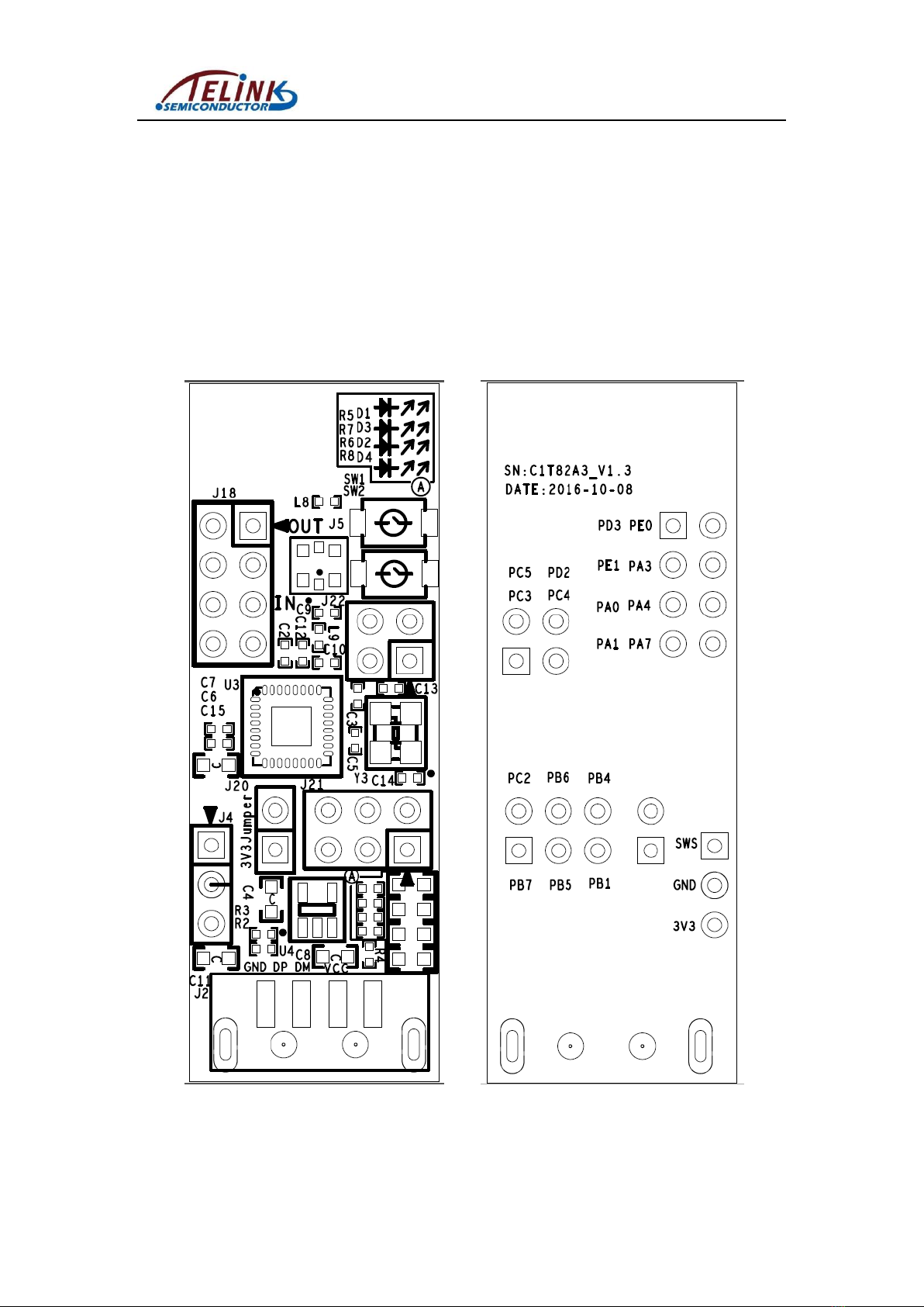
Figure 1 Dongle silkscreen (Left: Top view, Right: Bottom view)
User Guide for Telink TLSR8267 Debugging Dongle
AN-BLE-16090500-E2 5 Ver 1.1.0
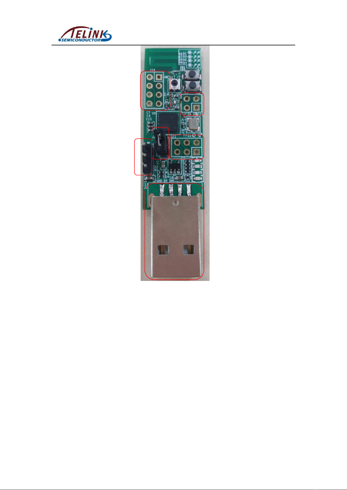
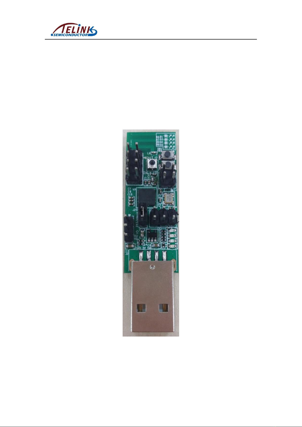
Figure 2 Dongle photo
For schematic (C1T82A3_V1.3) of TLSR8267 debugging dongle board, please
refer to Appendix.
4
3
2
1
SW1
SW2
J2
J4
1
2
3
J20
1
2
J18
1
2
1
3
3
4
5
3
7
3
6
8
J22
1
2
1
3
4
1
J21
2
1
3
3
5
3
4
1
6
J5
Not soldered by default.
Not soldered by default.
Not soldered by default.

User Guide for Telink TLSR8267 Debugging Dongle
AN-BLE-16090500-E2 6 Ver 1.1.0
2Pin Description
Table 1 Pin description
J2
1
VBUS
2
DM (PE2)
3
DP (PE3)
4
GND
S1
GND
S2
GND
J4
1
TL_SWS (PB0)
2
GND
3
3V3
J18
1
TL_PD3
2
TL_PE0
3
TL_PE1
4
TL_PA3
5
TL_PA0
6
TL_PA4
7
TL_PA1
8
TL_PA7
J20
1
VDDO3
2
3V3
J21
1
TL_PB7
2
TL_PWM2 (PC2)
3
TL_PB5
4
TL_PWM5 (PB6)
5
TL_PB1
6
TL_PWM4 (PB4)
J22
1
TL_PWM3 (PC3)
2
TL_PC5
3
TL_PC4
4
TL_PD2
SW1
TL_PD2
SW2
TL_PC5

User Guide for Telink TLSR8267 Debugging Dongle
AN-BLE-16090500-E2 7 Ver 1.1.0
3Pin Connection Guide
3.1 Supply power for 8267 Dongle
There are two connection methods to supply power for Telink TLSR8267
debugging dongle board.
1. Method 1:
Make sure a jumper cap is connected on J20 of 8267 Dongle.
Then connect J2 (USB interface) with PC USB.
2. Method 2:
Connect PIN2 and PIN3 of J4 with GND and 3.3V, respectively.
Figure 3 Connection chart to supply power
Option1:
1) Connect J20 with Jumper Cap;
2) Connect J2 with PC USB.
J20
J2
J4
2
3
Option 2:
1) Connect PIN2 with GND
2) Connect PIN3 with 3.3V

User Guide for Telink TLSR8267 Debugging Dongle
AN-BLE-16090500-E2 8 Ver 1.1.0
3.2 Download Firmware into 8267 Dongle
There are two connection methods to download firmware into Telink TLSR8267
debugging dongle board.
1. Method 1: Connect via USB
Make sure a jumper cap is connected on J20 of 8267 Dongle.
Connect J2 (USB interface) with the USB interface of a burning EVK board. The
miniUSB interface of the burning EVK is connected with PC USB via an USB cable.
2. Method 2: Connect via Swire
Connect PIN1, PIN2 and PIN3 of J4 with SWM, GND and 3.3V of a burning EVK,
respectively.
Figure 4 Connection chart to download FW
Option1:
1) Connect J20 with Jumper Cap;
2) Connect J2 with USB of burning EVK.
J20
J2
J4
2
3
Option 2: Connect J4 with
burning EVK via Swire.
1) Connect PIN1 with SWM
2) Connect PIN2 with GND
3) Connect PIN3 with 3.3V
1

User Guide for Telink TLSR8267 Debugging Dongle
AN-BLE-16090500-E2 9 Ver 1.1.0
3.3 Measure power-saving mode current for 8267 Dongle
To measure current consumption of Telink TLSR8267 debugging dongle board in
deep sleep or suspend mode, please follow the connection steps below:
1) Remove jumper cap from J20 of 8267 dongle, as shown in Figure 5.
2) Connect anode (+) and cathode (-) of an amperemeter with anode (+) of 3.3V
power supply and PIN3 of J4, respectively.
3) Connect cathode (-) of the 3.3V power supply with PIN2 of J4.
Figure 5 Connection chart to test sleep current
Remove jumper cap from J20
Connect PIN2 with
3.3V power supply --
Connect PIN3 with
Amperemeter --
J20
J4

User Guide for Telink TLSR8267 Debugging Dongle
AN-BLE-16090500-E2 10 Ver 1.1.0
3.4 Test RF signal for 8267 Dongle
To test RF signal for Telink TLSR8267 debugging dongle board, the J5 should be
connected with a spectrum analyzer via a RF cable (supplied by Telink).
Figure 6 Connection chart to test RF signal
Connect J5
Connect spectrum analyzer
J5
User Guide for Telink TLSR8267 Debugging Dongle
AN-BLE-16090500-E2 11 Ver 1.1.0
3.5 Test GPIOs for 8267 Dongle
Since all GPIOs of Telink TLSR8267 debugging dongle board are already
connected to corresponding pins of headers including J4, J18, J21 and J22, user can
directly test GPIO signals on header pins.
Note:
Only J4 and J20 are soldered on 8267 debugging dongle demo board supplied by
Telink. User needs to solder J18, J21 and J22 for development purpose.
Figure 7 Test GPIO signals on header pins
J4
SWS
GND
3V3
J18
PD3
PE0
J22
J21
PC2
PB7
PB5
3
PB1
3
PB6
1
PB4
PE1
PA3
PA0
PA4
PA1
PA7
PC3
PC5
PC4
3
PD2
3
J20

User Guide for Telink TLSR8267 Debugging Dongle
AN-BLE-16090500-E2 12 Ver 1.1.0
FCC COMPLIANCE STATEMENT:
This device complies with part 15 of the FCC Rules. Operation is
subject to the following two conditions: (1) This device may not
cause harmful interference, and (2) this device must accept any
interference received, including interference that may cause
undesired operation.
Changes or modifications not expressly approved by the party
responsible for compliance could void the user's authority to
operate the equipment.
Table of contents
Other TELINK SEMICONDUCTOR Computer Accessories manuals


