Teridian 71M6513H User manual

71M6513/71M6513H Demo Board
USER’S MANUAL
4/9/2007 10:06 AM
Revision 5.6
TERIDIAN Semiconductor Corporation
6440 Oak Canyon Rd.
Irvine, CA 92618-5201
Phone: (714) 508-8800 ▪Fax: (714) 508-8878
http://www.teridian.com/

71M6513/71M6513H Demo Board User’s Manual
Page: 2 of 112 © 2005-2006 TERIDIAN Semiconductor Corporation Revision 5.6
TERIDIAN Semiconductor Corporation makes no warranty for the use of its products, other than expressly contained in the Company’s
warranty detailed in the TERIDIAN Semiconductor Corporation standard Terms and Conditions. The company assumes no responsibility
for any errors which may appear in this document, reserves the right to change devices or specifications detailed herein at any time
without notice and does not make any commitment to update the information contained herein.

71M6513/71M6513H Demo Board User’s Manual
Page: 3 of 112 © 2005-2006 TERIDIAN Semiconductor Corporation Revision 5.6
71M6513/71M6513H
3-Phase Energy Meter IC
DEMO BOARD
USER’S MANUAL

71M6513/71M6513H Demo Board User’s Manual
Page: 4 of 112 © 2005-2006 TERIDIAN Semiconductor Corporation Revision 5.6
Table of Contents
1GETTING STARTED.............................................................................................................................................. 9
1.1 General .................................................................................................................................................................. 9
1.2 Safety and ESD Notes .......................................................................................................................................... 9
1.3 Demo Kit Contents ............................................................................................................................................. 10
1.4 Demo Board Versions ........................................................................................................................................ 10
1.5 Compatibility....................................................................................................................................................... 10
1.6 Suggested Equipment not Included ................................................................................................................. 10
1.7 Demo Board Test Setup..................................................................................................................................... 11
1.7.1 Power Supply Setup...................................................................................................................................... 14
1.7.2 Cable for Serial Connection (Debug Board) .................................................................................................. 14
1.7.3 Checking Operation....................................................................................................................................... 14
1.7.4 Serial Connection Setup................................................................................................................................ 15
1.8 Using the Demo Board....................................................................................................................................... 16
1.8.1 Serial Command Language........................................................................................................................... 17
1.8.2 Using the Demo Board for Energy Measurements ........................................................................................ 26
1.8.3 Adjusting the Kh Factor for the Demo Board................................................................................................. 26
1.8.4 Adjusting the Demo Boards to Different Current Transformers .....................................................................27
1.8.5 Adjusting the Demo Boards to Different Voltage Dividers ............................................................................. 27
1.9 Calibration Parameters ...................................................................................................................................... 28
1.9.1 General Calibration Procedure ...................................................................................................................... 28
1.9.2 Calibration Macro File ................................................................................................................................... 29
1.9.3 Updating the 6513_demo.hex file.................................................................................................................. 29
1.9.4 Updating Calibration Data in Flash Memory without Using the ICE or a Programmer................................... 29
1.9.5 Automatic Gains Calibration.......................................................................................................................... 30
1.9.6 Loading the 6513_demo.hex file into the Demo Board.................................................................................. 30
1.9.7 The Programming Interface of the 71M6513/6513H ..................................................................................... 32
1.10 Demo Code...................................................................................................................................................... 33
1.10.1 Demo Code Description............................................................................................................................. 33
1.10.2 Demo Code MPU Parameters ................................................................................................................... 34
1.10.3 Useful CLI Commands Involving the MPU and CE....................................................................................40
1.10.4 Demo Code for Neutral Detection (Demo Board D6513T3C1) .................................................................. 40
2APPLICATION INFORMATION ........................................................................................................................... 43
2.1 Calibration Theory.............................................................................................................................................. 43
2.1.1 Calibration with Three Measurements........................................................................................................... 43
2.1.2 Calibration with Five Measurements.............................................................................................................. 45
2.2 Calibration Procedures...................................................................................................................................... 46
2.2.1 Calibration Procedure with Three Measurements ......................................................................................... 47
2.2.2 Calibration Procedure with Five Measurements ............................................................................................ 48
2.2.3 Calibration Procedure for Rogowski Coil Sensors......................................................................................... 48
2.2.4 Calibration Spreadsheets .............................................................................................................................. 49
2.2.5 Compensating for Non-Linearities ................................................................................................................. 53

71M6513/71M6513H Demo Board User’s Manual
Page: 5 of 112 © 2005-2006 TERIDIAN Semiconductor Corporation Revision 5.6
2.3 Power Saving Measures .................................................................................................................................... 54
2.4 Schematic Information....................................................................................................................................... 55
2.4.1 Components for the V1 Pin ........................................................................................................................... 55
2.4.2 Reset Circuit.................................................................................................................................................. 55
2.4.3 Oscillator ....................................................................................................................................................... 56
2.4.4 EEPROM....................................................................................................................................................... 56
2.4.5 LCD............................................................................................................................................................... 57
2.4.6 Optical Interface ............................................................................................................................................ 58
2.4.7 Connecting the RX Pin .................................................................................................................................. 59
2.4.8 Connecting the V3 Pin................................................................................................................................... 60
2.5 Testing the Demo Board .................................................................................................................................... 61
2.5.1 Functional Meter Test.................................................................................................................................... 61
2.5.2 EEPROM....................................................................................................................................................... 62
2.5.3 RTC............................................................................................................................................................... 63
2.5.4 Hardware Watchdog Timer............................................................................................................................ 63
2.5.5 LCD............................................................................................................................................................... 63
2.6 TERIDIAN Application Notes ............................................................................................................................. 64
3HARDWARE DESCRIPTION............................................................................................................................... 65
3.1 D6513T3B2 Board Description: Jumpers, Switches and Test Points............................................................ 65
3.2 D6513T3C1 Board Description: Jumpers, Switches and Test Points............................................................ 69
3.3 D6513T3D2 Board Description: Jumpers, Switches and Test Points............................................................ 72
3.4 Board Hardware Specifications (D6513T3B2, D6513T3C1)............................................................................. 75
3.5 Board Hardware Specifications (D6513T3D2).................................................................................................. 76
4APPENDIX ........................................................................................................................................................... 77
List of Figures
Figure 1-1: TERIDIAN D6513T3B2 Demo Board with Debug Board: Basic Connections ................................................. 11
Figure 1-2: Block diagram for the TERIDIAN D6513T3B2 Demonstration Meter with Debug Board................................. 12
Figure 1-3: Block diagram for the TERIDIAN D6513T3C1 and D6513T3D2 Demo Boards with Debug Board................. 13
Figure 1-4: Hyperterminal Sample Window with Disconnect Button (Arrow) ..................................................................... 15
Figure 1-5: Port Speed and Handshake Setup (left) and Port Bit setup (right).................................................................. 16
Figure 1-6: Command Line Help Display........................................................................................................................... 17
Figure 1-7: Typical Calibration Macro file .......................................................................................................................... 29
Figure 1-8: Emulator Window Showing Reset and Erase Buttons (see Arrows) ............................................................... 31
Figure 1-9: Emulator Window Showing Erased Flash Memory and File Load Menu......................................................... 31
Figure 2-1: Watt Meter with Gain and Phase Errors.......................................................................................................... 43
Figure 2-2: Phase Angle Definitions.................................................................................................................................. 47
Figure 2-3: Calibration Spreadsheet for Three Measurements ......................................................................................... 51
Figure 2-4: Calibration Spreadsheet for Five Measurements ............................................................................................ 51
Figure 2-5: Calibration Spreadsheet for Rogowski coil...................................................................................................... 52
Figure 2-6: Non-Linearity Caused by Quantification Noise................................................................................................ 53
Figure 2-7: Voltage Divider for V1 ..................................................................................................................................... 55
Figure 2-8: External Components for RESETZ ................................................................................................................. 55

71M6513/71M6513H Demo Board User’s Manual
Page: 6 of 112 © 2005-2006 TERIDIAN Semiconductor Corporation Revision 5.6
Figure 2-9: Oscillator Circuit.............................................................................................................................................. 56
Figure 2-10: EEPROM Circuit ........................................................................................................................................... 56
Figure 2-11: LCD Connections.......................................................................................................................................... 57
Figure 2-12: LCD Boost and LCD Control Registers......................................................................................................... 57
Figure 2-13: Optical Interface Block Diagram.................................................................................................................... 58
Figure 2-14: Optical Port Circuitry on the D6513T3B2 Demo Board ................................................................................. 58
Figure 2-15: Optical Port Circuitry on the D6513T3C1 Demo Board................................................................................. 59
Figure 2-16: Internal Diode Clamp on the RX Pin ............................................................................................................. 59
Figure 2-17: Resistor Network for RX................................................................................................................................ 60
Figure 2-18: Meter with Calibration System ...................................................................................................................... 61
Figure 2-19: Calibration System Screen............................................................................................................................ 62
Figure 3-1: D6513T3B2 Demo Board - Board Description (Default jumper settings indicated in yellow)........................... 68
Figure 3-2: D6513T3C1 Demo Board - Board Description ................................................................................................ 71
Figure 3-3: D6513T3D2 Demo Board - Board Description ................................................................................................ 74
Figure 4-1: TERIDIAN D6513T3B2 Demo Board: Electrical Schematic 1/3 ...................................................................... 78
Figure 4-2: TERIDIAN D6513T3B2 Demo Board: Electrical Schematic 2/3 ...................................................................... 79
Figure 4-3: TERIDIAN D6513T3B2 Demo Board: Electrical Schematic 2/3 ...................................................................... 80
Figure 4-4: TERIDIAN D6513T3C1 Demo Board: Electrical Schematic 1/3...................................................................... 81
Figure 4-5: TERIDIAN D6513T3C1 Demo Board: Electrical Schematic 2/3...................................................................... 82
Figure 4-6: TERIDIAN D6513T3C1 Demo Board: Electrical Schematic 3/3...................................................................... 83
Figure 4-7: TERIDIAN D6513T3D2 Demo Board: Electrical Schematic 1/3...................................................................... 84
Figure 4-8: TERIDIAN D6513T3D2 Demo Board: Electrical Schematic 2/3...................................................................... 85
Figure 4-9: TERIDIAN D6513T3D2 Demo Board: Electrical Schematic 3/3...................................................................... 86
Figure 4-10: TERIDIAN D6513T3B2 Demo Board: Top View ........................................................................................... 90
Figure 4-11: TERIDIAN D6513T3B2 Demo Board: Bottom View ...................................................................................... 91
Figure 4-12: TERIDIAN D6513T3B2 Demo Board: Top Signal Layer ............................................................................... 92
Figure 4-13: TERIDIAN D6513T3B2 Demo Board: Middle Layer 1 (Ground Plane) ......................................................... 93
Figure 4-14: TERIDIAN D6513T3B2 Demo Board: Middle Layer 2 (Supply Plane) .......................................................... 94
Figure 4-15: TERIDIAN D6513T3B2 Demo Board: Bottom Signal Layer .......................................................................... 95
Figure 4-16: TERIDIAN D6513T3C1 Demo Board: Top View........................................................................................... 96
Figure 4-17: TERIDIAN D6513T3C1 Demo Board: Bottom View...................................................................................... 97
Figure 4-18: TERIDIAN D6513T3C1 Demo Board: Top Signal Layer ............................................................................... 98
Figure 4-19: TERIDIAN D6513T3C1 Demo Board: Ground Plane Layer .......................................................................... 99
Figure 4-20: TERIDIAN D6513T3C1 Demo Board: Power Plane Layer.......................................................................... 100
Figure 4-21: TERIDIAN D6513T3C1 Demo Board: Bottom Signal Layer........................................................................ 101
Figure 4-22: TERIDIAN D6513T3D2 Demo Board: Top Signal Layer ............................................................................. 102
Figure 4-23: TERIDIAN D6513T3D2 Demo Board: Bottom Signal Layer........................................................................ 103
Figure 4-24: TERIDIAN D6513T3D2 Demo Board: Bottom View.................................................................................... 104

71M6513/71M6513H Demo Board User’s Manual
Page: 7 of 112 © 2005-2006 TERIDIAN Semiconductor Corporation Revision 5.6
Figure 4-25: Debug Board: Electrical Schematic............................................................................................................. 106
Figure 4-26: Debug Board: Top View.............................................................................................................................. 107
Figure 4-27: Debug Board: Bottom View......................................................................................................................... 107
Figure 4-28: Debug Board: Top Signal Layer.................................................................................................................. 108
Figure 4-29: Debug Board: Middle Layer 1 (Ground Plane) ............................................................................................ 108
Figure 4-30: Debug Board: Middle Layer 2 (Supply Plane) ............................................................................................. 109
Figure 4-31: Debug Board: Bottom Trace Layer ............................................................................................................. 109
Figure 4-32: TERIDIAN 71M6513/71M6513H epLQFP100: Pinout (top view) ................................................................ 112
List of Tables
Table 1-1: Jumper settings on Debug Board..................................................................................................................... 14
Table 1-2: Straight cable connections ............................................................................................................................... 14
Table 1-3: Null-modem cable connections ........................................................................................................................ 14
Table 1-4: CE RAM Locations for Calibration Constants................................................................................................... 28
Table 1-5: Flash Programming Interface Signals .............................................................................................................. 32
Table 1-6: MPU Input Parameters for Metering................................................................................................................. 35
Table 1-7: MPU Input Parameters for Temperature Compensation .................................................................................. 35
Table 1-8: MPU Parameters for Pulse Source Selection................................................................................................... 36
Table 1-9: Selectable Pulse Sources ................................................................................................................................ 36
Table 1-10: MPU Instantaneous Output Variables ............................................................................................................ 37
Table 1-11: MPU Status Word Bit Assignment.................................................................................................................. 38
Table 1-12: MPU Accumulation Output Variables ............................................................................................................. 39
Table 1-13: CLI Commands for MPU Data Memory.......................................................................................................... 40
Table 1-14: Neutral Current Accuracy at Various Sampling Frequencies ......................................................................... 41
Table 2-1: Power Saving Measures .................................................................................................................................. 54
Table 3-1: D6513T3B2 Demo Board Description .............................................................................................................. 65
Table 3-2: D6513T3B2 Demo Board Description .............................................................................................................. 66
Table 3-3: D6513T3B2 Demo Board Description .............................................................................................................. 67
Table 3-4: D6513T3C1 Demo Board Description.............................................................................................................. 69
Table 3-5: D6513T3C1 Demo Board Description.............................................................................................................. 70
Table 3-6: D6513T3D2 Demo Board Description.............................................................................................................. 73
Table 4-1: D6513T3C1 Demo Board: Bill of Material ........................................................................................................ 87
Table 4-2: D6513T3B2 Demo Board: Bill of Material ........................................................................................................ 88
Table 4-3: D6513T3D2 Demo Board: Bill of Material ........................................................................................................ 89
Table 4-4: Debug Board: Bill of Material.......................................................................................................................... 105
Table 4-5: 71M6513/71M6513H Pin Description Table 1/3............................................................................................. 110
Table 4-6: 71M6513/71M6513H Pin Description Table 2/3............................................................................................. 110
Table 4-7: 71M6513/71M6513H Pin Description Table 3/3............................................................................................. 111

71M6513/71M6513H Demo Board User’s Manual
Page: 8 of 112 © 2005-2006 TERIDIAN Semiconductor Corporation Revision 5.6

71M6513/71M6513H Demo Board User’s Manual
Page: 9 of 112 © 2005-2006 TERIDIAN Semiconductor Corporation Revision 5.6
1 GETTING STARTED
1.1 GENERAL
The TERIDIAN Semiconductor Corporation (TSC) 71M6513/71M6513H Demo Board is a demonstration board
for evaluating the 71M6513/71M6513H device for 3-phase electronic power metering applications. It in-
corporates a 71M6513 or 71M6513H integrated circuit, peripheral circuitry such as a serial EEPROM, emulator
port, and on board power supply as well as a companion Debug Board that allows a connection to a PC through
a RS232 port. The demo board allows the evaluation of the 71M6513 or 71M6513H energy meter chip for
measurement accuracy and overall system use.
The board is pre-programmed with a Demo Program (file name 6513_demo.hex) in the FLASH memory of the
71M6513/6513H IC. This embedded application is developed to exercise all low-level function calls to directly
manage the peripherals, flash programming, and CPU (clock, timing, power savings, etc.).
The 71M6513/6513H IC on the Demo Board is pre-programmed with default calibration factors.
1.2 SAFETY AND ESD NOTES
Connecting live voltages to the demo board system will result in potentially hazardous voltages on the demo
board.
BEFORE OPERATING THE DEMO BOARD, THE JUMPERS ON JP2 AND JP3 (IF IN-
STALLED) SHOULD BE REMOVED! IT IS RECOMMENDED TO OPERATE THE
DEBUG BOARD WITH ITS OWN POWER SUPPLY.
THE DEMO SYSTEM IS ESD SENSITIVE! ESD PRECAUTIONS SHOULD BE TAKEN
WHEN HANDLING THE DEMO BOARD!
EXTREME CAUTION SHOULD BE TAKEN WHEN HANDLING THE DEMO BOARD
ONCE IT IS CONNECTED TO LIVE VOLTAGES!
1

71M6513/71M6513H Demo Board User’s Manual
Page: 10 of 112 © 2005-2006 TERIDIAN Semiconductor Corporation Revision 5.6
1.3 DEMO KIT CONTENTS
• Demo Board with 71M6513/71M6513H IC and pre-loaded demo program:
• D6513T3B2 Demo Board (standard poly-phase), or
• D6513T3C1 Demo Board (poly-phase w/ added neutral current capability)
• Debug Board
• Two 5VDC/1,000mA universal wall transformers with 2.5mm plug (Switchcraft 712A compatible)
• Serial cable, DB9, Male/Female, 2m length (Digi-Key AE1020-ND)
• CD-ROM containing documentation (data sheet, board schematics, BOM, layout), Demo Code (sources
and executable), and utilities
The CD-ROM contains a file named readme.txt that specifies all files found on the media and their
purpose.
1.4 DEMO BOARD VERSIONS
The following versions of the Demo Board are available:
• Demo Board D6513T3B2 (standard)
• Demo Board D6513T3C1 (with neutral current detection capability)
• Demo Board D6513T3D2 (two layer PCB, with neutral current detection capability)
1.5 COMPATIBILITY
This manual applies to the following hardware and software revisions:
• 71M6513 or 71M6513H chip revision B03
• Demo Kit firmware revision 3.04 and 3.05 or later
• Demo Boards D6513T3B2, D6513T3C1 and D6513T3D2
1.6 SUGGESTED EQUIPMENT NOT INCLUDED
For functional demonstration:
• PC w/ MS-Windowsversions XP, ME, or 2000, equipped with RS232 port (COM port) via DB9 connector
For software development (MPU code):
• Signum ICE (In Circuit Emulator): ADM-51
http://www.signum.com
• Keil 8051 “C” Compiler kit: CA51
http://www.keil.com/c51/ca51kit.htm, http://www.keil.com/product/sales.htm

71M6513/71M6513H Demo Board User’s Manual
Page: 11 of 112 © 2005-2006 TERIDIAN Semiconductor Corporation Revision 5.6
1.7 DEMO BOARD TEST SETUP
Figure 1-1 shows the basic connections of the Demo Board plus Debug Board with the external equipment for
desktop testing, i.e. without live power applied. For desktop testing, both the Demo and Debug board may be
powered with just the 5VDC power supplies.
Host PC
Debug
Board
Demo Board
Power Supply
(100 to 240VAC,
1ADC Output)
Power
Power
Figure 1-1: TERIDIAN D6513T3B2 Demo Board with Debug Board: Basic Connections
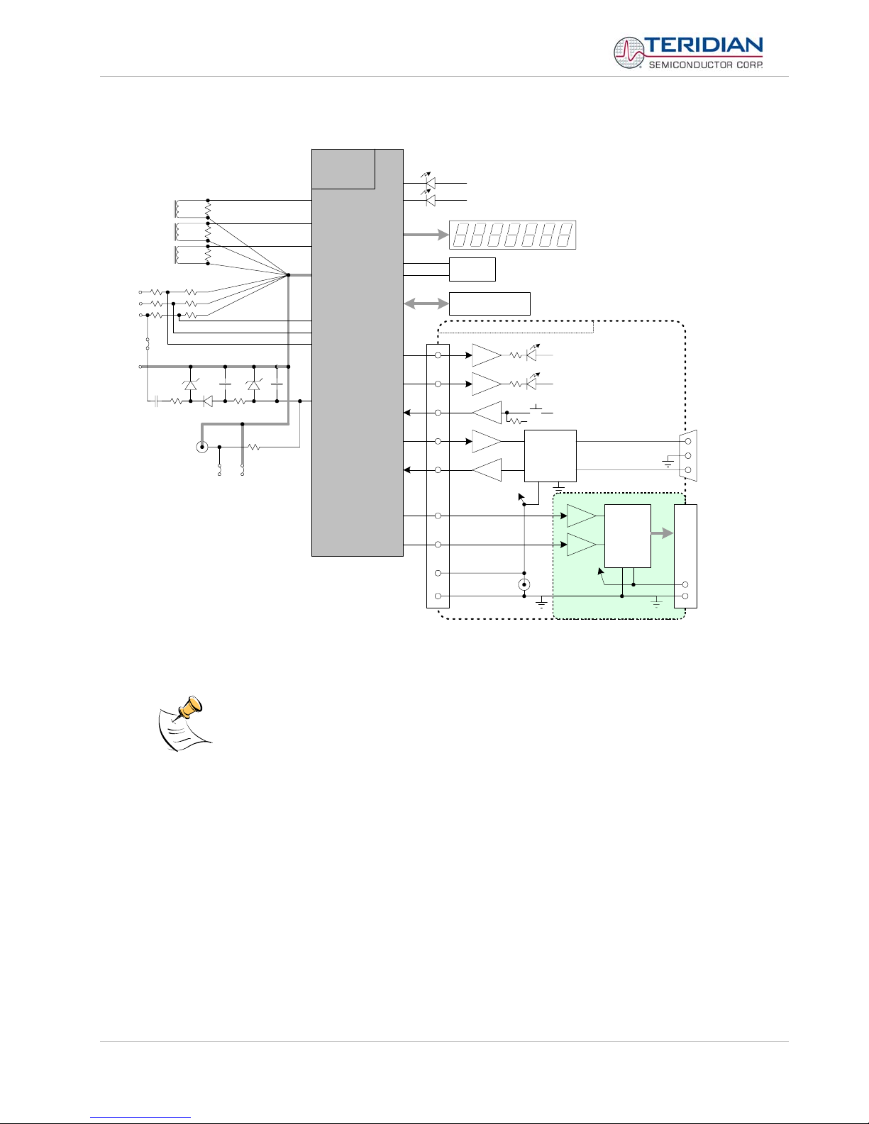
The D6513/T3B2 Demo Board block diagram is shown in Figure 1-2. It consists of a stand-alone (round) meter
Demo Board and an optional Debug Board. The Demo Board contains all circuits necessary for operation as a
meter, including display, calibration LED, and internal power supply. The Debug Board, when using a separate
power supply, is optically isolated from the meter and interfaces to a PC through a 9 pin serial port. For serial
communication between the PC and the TERIDIAN 71M6513/71M6513H, the Debug Board needs to be
plugged with its connector J3 into connector J2 of the Demo Board.
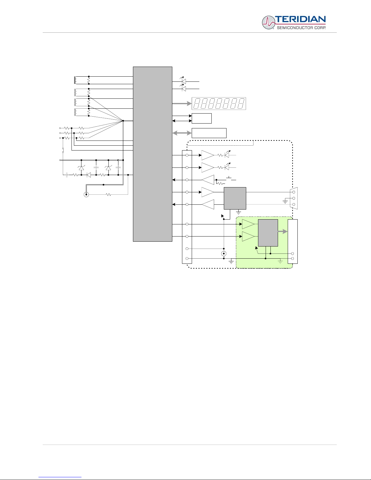
The D6513/T3C1 Demo Board System is shown in Figure 1-3. It is almost identical to the D6513T3B2, except
that the neutral current input is added and the optional power and ground connections from the Demo Board to
the Debug Board were removed.
Connections to the external signals to be measured, i.e. scaled AC voltages and current signals derived from
shunt resistors or current transformers, are provided on the rear side of the demo board.
Caution: It is recommended to set up the demo board with no live AC voltage
connected, and to connect live AC voltages only after the user is familiar with
the demo system.
71M6513/71M6513H Demo Board User’s Manual
Page: 12 of 112 © 2005-2006 TERIDIAN Semiconductor Corporation Revision 5.6
DEMONSTRATION METER
IA
IB
IC
VC
VB
NEUT
IA
IB
IC
V3P3
VC
VB
VA
3.3v
VA
GND
V3P3
GND
JP1
5V
DC
EEPROM
V3P3
V3P3
ICE Connector
JP2 JP3
OPTO
OPTO
OPTO
OPTO
OPTO
WATT
VAR
DIO0
DIO1
DIO2
TX
RX
5V DC
V5_DBG
GND_DBG
V5_DBG
V5_DBG
OPTO SUPPLY
RS-232
INTERFACE
DB9
to PC
COM Port
GND_DBG
CYCLE DISPLAY
V5_DBG
OPTO
OPTO
FPGA
J5
68 Pin Connector
to NI PCI-6534
DIO Board
OPTO SUPPLY
V5_NI
CE HEARTBEAT (1Hz)
MPU HEARTBEAT (5Hz)
DEBUG BOARD (OPTIONAL)
6513
Single Chip
Meter
TMUXOUT
CKTEST
5V LCD DISPLAY
DIO4
DIO5
DIO6
DIO7
RTM INTERFACE
PULSE OUTPUTS
External Current
Transformers
Figure 1-2: Block diagram for the TERIDIAN D6513T3B2 Demonstration Meter with Debug Board
All input signals are referenced to the V3P3 (3.3V power supply to the chip).
71M6513/71M6513H Demo Board User’s Manual
Page: 13 of 112 © 2005-2006 TERIDIAN Semiconductor Corporation Revision 5.6
DEMONSTRATION METER
IA
IB
IC
VC
VB
NEUT
IA
IB
IC
V3P3
VC
VB
VA
3.3v
VA
GND
V3P3
GND
JP1
5V
DC
EEPROM
V3P3
V3P3
ICE Connector
OPTO
OPTO
OPTO
OPTO
OPTO
WATT
VAR
DIO0
DIO1
DIO2
TX
RX
5V DC
V5_DBG
GND_DBG
V5_DBG
V5_DBG
OPTO SUPPLY
RS-232
INTERFACE
DB9
to PC
COM Port
GND_DBG
CYCLE DISPLAY
V5_DBG
OPTO
OPTO
FPGA
(optional)
J5
68 Pin Connector
to NI PCI-6534
DIO Board
OPTO SUPPLY
V5_NI
CE HEARTBEAT (1Hz)
MPU HEARTBEAT (5Hz)
DEBUG BOARD (OPTIONAL)
6513
Single Chip
Meter
TMUXOUT
CKTEST
5V LCD DISPLAY
DIO4
DIO5
DIO6
DIO7
OPTIONAL
RTM INTERFACE
V3
VBIAS
INEUTRAL
PULSE OUTPUTS
External Current
Transformers
Figure 1-3: Block diagram for the TERIDIAN D6513T3C1 and D6513T3D2 Demo Boards with Debug Board

71M6513/71M6513H Demo Board User’s Manual
Page: 14 of 112 © 2005-2006 TERIDIAN Semiconductor Corporation Revision 5.6
1.7.1 POWER SUPPLY SETUP
There are several choices for meter power supply:
• Internal (using phase A of the AC line voltage). The internal power supply is only suitable when phase A
exceeds 220V RMS.
• External 5VDC connector (J1) on the Demo Board
• External 5VDC connector (J1) on the Debug Board.
The three power supply jumpers, JP1, JP2, and JP3 (JP2/JP3 is only provided on the D6513T3B2
Demo Board), must be consistent with the power supply choice. JP1 connects the AC line voltage to
the internal power supply. This jumper should usually be left in place. JP2 and JP3 should be left
open (unconnected).
1.7.2 CABLE FOR SERIAL CONNECTION (DEBUG BOARD)
For connection of the DB9 serial port to a PC, either a straight or a so-called “null-modem” cable may be used.
JP1 and JP2 are plugged in for the straight cable, and JP3/JP4 are empty. The jumper configuration is reversed
for the null-modem cable, as shown in Table 1-1.
Jumpers on Debug Board
Cable
Configuration Mode JP1 JP2 JP3 JP4
Straight Cable Default Installed Installed -- --
Null-Modem Cable Alternative -- -- Installed Installed
Table 1-1: Jumper settings on Debug Board
JP1 through JP4 can also be used to alter the connection when the PC is not configured as a DCE device.
Table 1-2 shows the connections necessary for the straight DB9 cable and the pin definitions.
PC Pin Function Demo Board Pin
2 TX 2
3 RX 3
5 Signal Ground 5
Table 1-2: Straight cable connections
Table 1-3 shows the connections necessary for the null-modem DB9 cable and the pin definitions.
PC Pin Function Demo Board Pin
2 TX 3
3 RX 2
5 Signal Ground 5
Table 1-3: Null-modem cable connections
1.7.3 CHECKING OPERATION
A few seconds after power up, the LCD display on the Demo Board should display this brief greeting:
H E L L 0

71M6513/71M6513H Demo Board User’s Manual
Page: 15 of 112 © 2005-2006 TERIDIAN Semiconductor Corporation Revision 5.6
The “HELLO” message should be followed by the display of accumulated energy:
3. 0. 0 0 1
The decimal dot in the leftmost segment will be blinking, indicating activity of the MPU inside the
71M6513/6513H.
If contacts 3 and 5 of J2 are shorted with a jumper (or if the “DISPLAY SEL” switch SW2 on the Debug Board is
pressed and held down), the display will show a series of incrementing numbers (1 through 12) in the leftmost
digit(s) followed by the default date (2001.01.01) at number 10.
Once, the Debug Board is plugged into J2 of the Demo Board, LED DIO1 on the Debug Board will flash with a
frequency of 1Hz, indicating CE activity. The LED DIO0 will flash with a frequency of 5Hz, indicating MPU
activity.
1.7.4 SERIAL CONNECTION SETUP
After connecting the DB9 serial port to a PC, start the HyperTerminal application and create a session using the
following parameters:
Port Speed: 9600 baud
Data Bits: 8
Parity: None
Stop Bits: 1
Flow Control: XON/XOFF
HyperTerminal can be found by selecting Programs ÆAccessories ÆCommunications from the Windowsstart
menu. The connection parameters are configured by selecting File ÆProperties and then by pressing the
Configure button. Port speed and flow control are configured under the General tab (Figure 1-5, left), bit settings
are configured by pressing the Configure button (Figure 1-6, right), as shown below. A setup file (file name
“Demo Board Connection.ht”) for HyperTerminal that can be loaded with File ÆOpen is also provided with the
tools and utilities.
Port parameters can only be adjusted when the connection is not active. The disconnect
button, as shown in Figure 1-4 must be clicked in order to disconnect the port.
Figure 1-4: Hyperterminal Sample Window with Disconnect Button (Arrow)

71M6513/71M6513H Demo Board User’s Manual
Page: 16 of 112 © 2005-2006 TERIDIAN Semiconductor Corporation Revision 5.6
Figure 1-5: Port Speed and Handshake Setup (left) and Port Bit setup (right)
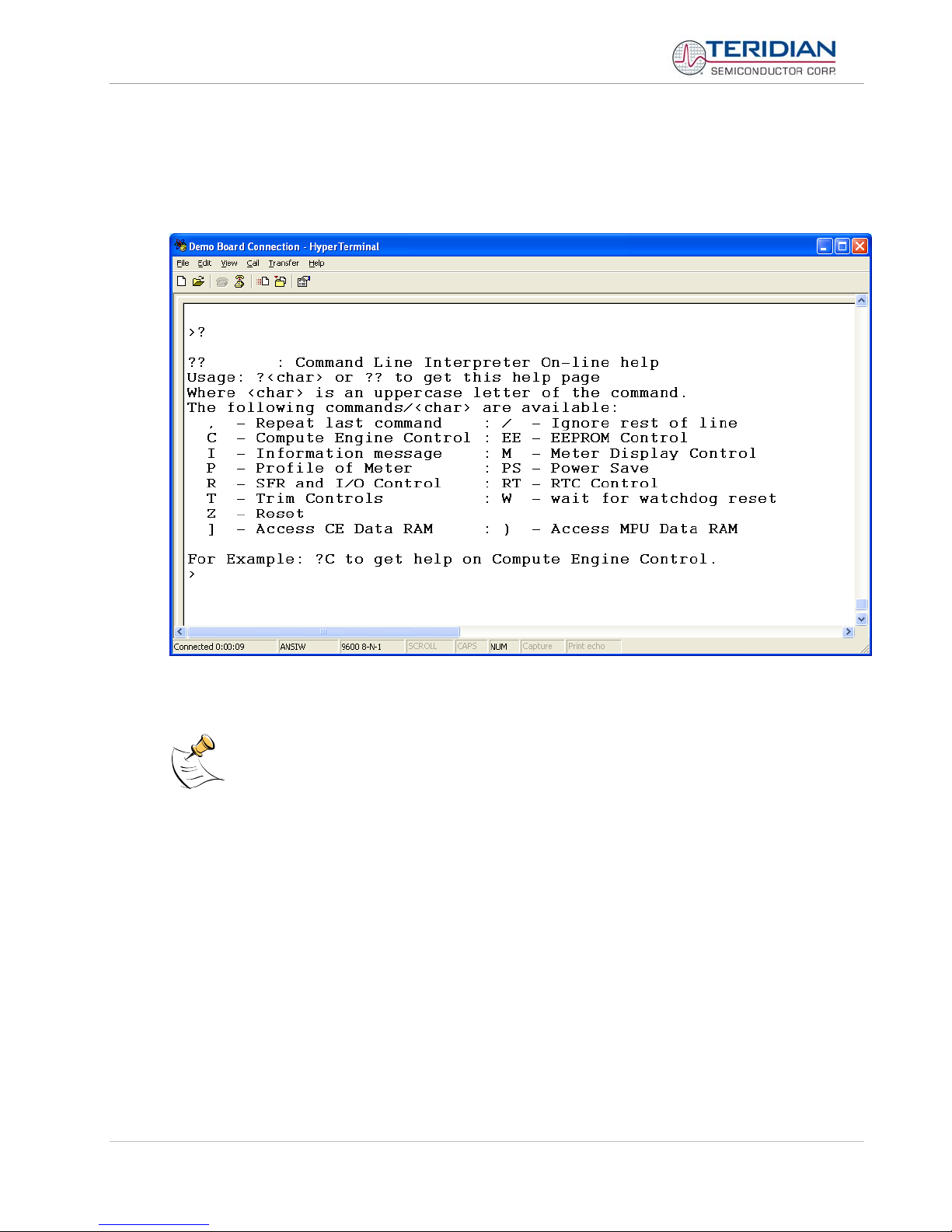
Once, the connection to the demo board is established, press <CR> and the prompt, >, should appear. Type
>? to see the Demo Code help menu. Type >i1 to verify that the demo code revision is 3.04 or later.
1.8 USING THE DEMO BOARD
The 71M6513/6513H Demo Board is a ready-to-use meter prepared for use with an external current trans-
former.
Using the Demo Board involves communicating with the Demo Code via the command line interface (CLI). The
CLI allows all sorts of manipulations to the metering parameters, access to the EEPROM, initiation of auto-cal
sequences, selection of the displayed parameters, changing calibration factors and many more operations.
Before evaluating the 71M6513/6513H on the Demo Board, users should get familiar with the commands and
responses of the CLI. A complete description of the CLI is provided in section 1.8.1.
71M6513/71M6513H Demo Board User’s Manual
Page: 17 of 112 © 2005-2006 TERIDIAN Semiconductor Corporation Revision 5.6
1.8.1 SERIAL COMMAND LANGUAGE
The Demo Code residing in the flash memory of the 71M6513/6513H provides a convenient way of examining
and modifying key meter parameters. Once the Demo Board is connected to a PC or terminal per the
instructions given in Section 1.7.2 and 1.7.4, typing ‘?’ will bring up the list of commands shown in Figure 1-6.
Figure 1-6: Command Line Help Display
The tables in this chapter describe the commands in detail.
Demo Code revision 3.05 offers more commands than revision 3.04. Commands only
available on 3.05 are marked in the tables presented in this chapter.
71M6513/71M6513H Demo Board User’s Manual
Page: 18 of 112 © 2005-2006 TERIDIAN Semiconductor Corporation Revision 5.6
Commands to Display Help on the CLI Commands:
? HELP
Description: Command help available for each of the options below.
Command
combinations: ? Command line interpreter help menu.
?] Display help on access CE data RAM
?) Display help on access MPU RAM
?, Display help on repeat last command
?/ Display help on ignore rest of line
?C Display help on compute engine control and calibration.
In 3.05, pulse counter functions are offered.
?EE Display help on EEPROM control
?I Display help on information message
?M Display help on meter display control
?P Display help on profile of meter
?R Display help on SFR control
?RT Display help on RTC control
?T Display help on trim control
?W Display help on the wait/reset command – 3.05 only
?Z Display help on reset
Examples: ?? Display the command line interpreter help menu.
?C Displays compute engine control help.
Commands for CE Data Access:
] CE DATA ACCESS
Description: Allows user to read from and write to CE data space.
Usage: ] [Starting CE Data Address] [option]…[option]
Command
combinations:
]A??? Read consecutive 16-bit words in Decimal, starting at
address A
]A$$$ Read consecutive 16-bit words in Hex, starting at address A
]A=n=n Write consecutive memory values, starting at address A
]U Update default version of CE Data in flash memory
Example: ]40$$$ Reads CE data words 0x40, 0x41 and 0x42.
]7E=12345678=9876ABCD Writes two words starting @ 0x7E
CE data space is the address range for the CE DRAM (0x1000 to 0x13FF). All CE data words are in 4-byte (32-
bit) format. The offset of 0x1000 does not have to be entered when using the ] command, thus typing ]A? will
access the 32-bit word located at the byte address 0x1000 + 4 * A = 0x1028.

71M6513/71M6513H Demo Board User’s Manual
Page: 19 of 112 © 2005-2006 TERIDIAN Semiconductor Corporation Revision 5.6
Commands for MPU/XDATA Access:
) MPU DATA ACCESS
Description: Allows user to read from and write to MPU data space.
Usage: ) [Starting MPU Data Address] [option]…[option]
Command
combinations:
)A??? Read three consecutive 32-bit words in Decimal, starting at
address A
)A$$$ Read three consecutive 32-bit words in Hex, starting at
address A
)A=n=m Write the values n and m to two consecutive addresses
starting at address A
Example: )08$$$$ Reads data words 0x08, 0x0C, 0x10, 0x14
)04=12345678=9876ABCD Writes two words starting @ 0x04
MPU or XDATA space is the address range for the MPU XRAM (0x0000 to 0x3FF). All MPU data words are in
4-byte (32-bit) format. Typing ]A? will access the 32-bit word located at the byte address 4 * A = 0x28. The
energy accumulation registers of the Demo Code can be accessed by typing two Dollar signs (“$$”), typing
question marks will display negative decimal values if the most significant bit is set.
RAM access is limited to the lower 1KB address range. Read and write operations will “wrap around”
at higher addresses, i.e. )200? will yield the same result as )0?
Commands for DIO RAM (Configuration RAM) and SFR Control:
R DIO AND SFR CONTROL
Description: Allows the user to read from and write to DIO RAM and special function registers (SFRs).
Usage: R [option] [register] … [option]
Command
combinations:
RIx… Select I/O RAM location x (0x2000 offset is automatically
added)
Rx… Select internal SFR at address x
Ra???... Read consecutive SFR registers in Decimal, starting at
address a
Ra$$$... Read consecutive registers in Hex, starting at address a
Ra=n=m… Set values of consecutive registers to n and m starting at
address a
Example: RI2$$$ Read DIO RAM registers 2, 3, and 4 in Hex.
DIO or Configuration RAM space is the address range 0x2000 to 0x20FF. This RAM contains registers used for
configuring basic hardware and functional properties of the 71M6513/6513H and is organized in bytes (8 bits).
The 0x2000 offset is automatically added when the command RI is typed.
The SFRs (special function registers) are located in internal RAM of the 80515 core, starting at address 0x80.

71M6513/71M6513H Demo Board User’s Manual
Page: 20 of 112 © 2005-2006 TERIDIAN Semiconductor Corporation Revision 5.6
Commands for EEPROM Control:
EE EEPROM CONTROL
Description: Allows user to enable read and write to EEPROM.
Usage: EE [option] [arguments]
Command
combinations:
EECn EEPROM Access (1 ÆEnable, 0 ÆDisable)
EERa.b Read EEPROM at address 'a' for 'b' bytes.
EESabc..xyz Write characters to buffer (sets Write length)
EETa Transmit buffer to EEPROM at address 'a'.
EEWa.b...z Write values to buffer
Example: EEShello
EET$0210
Writes 'hello' to buffer, then transmits buffer to EEPROM
starting at address 0x210.
Due to buffer size restrictions, the maximum number of bytes handled by the EEPROM command is
0x40.
Auxiliary Commands:
Typing a comma (“,”) repeats the command issued from the previous command line. This is very helpful when examining
the value at a certain address over time, such as the CE DRAM address for the temperature (0x40).
The slash (“/”) is useful to separate comments from commands when sending macro text files via the serial interface. All
characters in a line after the slash are ignored.
Commands controlling the CE, TMUX and the RTM:
C COMPUTE ENGINE
CONTROL
Description: Allows the user to enable and configure the compute engine.
Usage: C [option] [argument]
Command
combinations:
CEn Compute Engine Enable (1 ÆEnable,
0 ÆDisable)
CTn Select input n for TMUX output pin. n is interpreted as a
decimal number.
CREn RTM output control (1 ÆEnable, 0 ÆDisable)
CRSa.b.c.d Selects CE addresses for RTM output
Example: CE0 Disables CE, followed by “CE OFF” display on LCD. The
Demo Code will reset if the WD timer is enabled.
CT3 Selects the VBIAS signal for the TMUX output pin
This manual suits for next models
1
Table of contents
Popular Control Unit manuals by other brands

GEM
GEM eSyDrive R649 operating instructions

Lenze
Lenze L-force Communication ModemCAN EMF2181IB Communications manual

Pulsar
Pulsar EN54M Series user manual

EXAGATE
EXAGATE SYSGuard 4001 Quick installation guide

ARI
ARI D-040 Installation operation & maintenance

EnerSys
EnerSys OutBack Power SkyBox SBX5048-120/240 Technical and commissioning documentation


ZIEHL-ABEGG
ZIEHL-ABEGG UNIcon CPG AVC Series operating instructions

Fermax
Fermax SKYLINE LYNX DUOX Installer manual

VAMP
VAMP 259 Operation and configuration instructions

EFI
EFI EB-32 Installation and service guide

Comunello
Comunello CU 230V HP Installation and user manual

Weidmüller
Weidmüller AMS400A operating instructions