Tessera Technology AD-MS/PJ4 User manual

Motor Sensor Board
(AD-MS/PJ4)
Hardware Manual
Date published: July 2011 (First Edition)
Tessera Technology Inc.
- 1 -

CAUTION:
・ The information in this document is subject to change without notice.
・ No part of this document may be copied or reproduced in any form or by any means without
prior written consent of Tessera Technology Inc.
・ Tessera Technology Inc. assumes no responsibility for inaccuracies or misprints of this
document.
・ Tessera Technology Inc. does not license assurance or enforcement of intellectual property
rights and other rights of Tessera Technology Inc. and third parties by the use of the
products and/or the information in this document. Tessera Technology Inc. does not
assume any liability for infringement of rights of third parties by the use of the products
and/or the information in this document.
・ Descriptions of circuits, software and other related information in this document are
provided for illustrative purposes in semiconductor product operation and application
examples. The incorporation of these circuits, software and information in the design of a
customer's equipment shall be done under the full responsibility of the customer. Tessera
Technology Inc. assumes no responsibility for any losses incurred by customers or third
parties arising from the use of these circuits, software and information.
- 2 -

TABLE OF CONTENTS
1······································································································ 4Introduction
2··········································································································· 5Features
2.1
Resolver 1 I/O Connector (CN12)··········································································6
2.2
Motor Control 1 Connector (CN14) ········································································8
2.3
Analog Input Connector (CN7) ··············································································9
2.4
Digital I/O Connector (CN10) ············································································· 11
····································································································· 122.4.1 CAN
··································································································· 132.4.2 UART
·························································································· 152.4.3 Digital Output
····························································································· 162.4.4 Digital Input
2.5
Power Supply································································································· 17
- 3 -

1Introduction
This manual describes the features and hardware specifications of the Motor Sensor Board
(AD-MS/PJ4). The Motor Sensor Board is used with connecting to EB-850/PJ4E, which the 32-bit
single-chip microcomputer V850E2/PJ4-E from Renesas Electronics Corporation is mounted on.
- 4 -

2Features
CPU Board
Analog Input
Connector
Resolver 1
I/O Connector
Motor Control 1
Connector
Power
Digital I/O AC Adopter Input
CPU 用ボード接続
CPU Board
Connectors
- 5 -
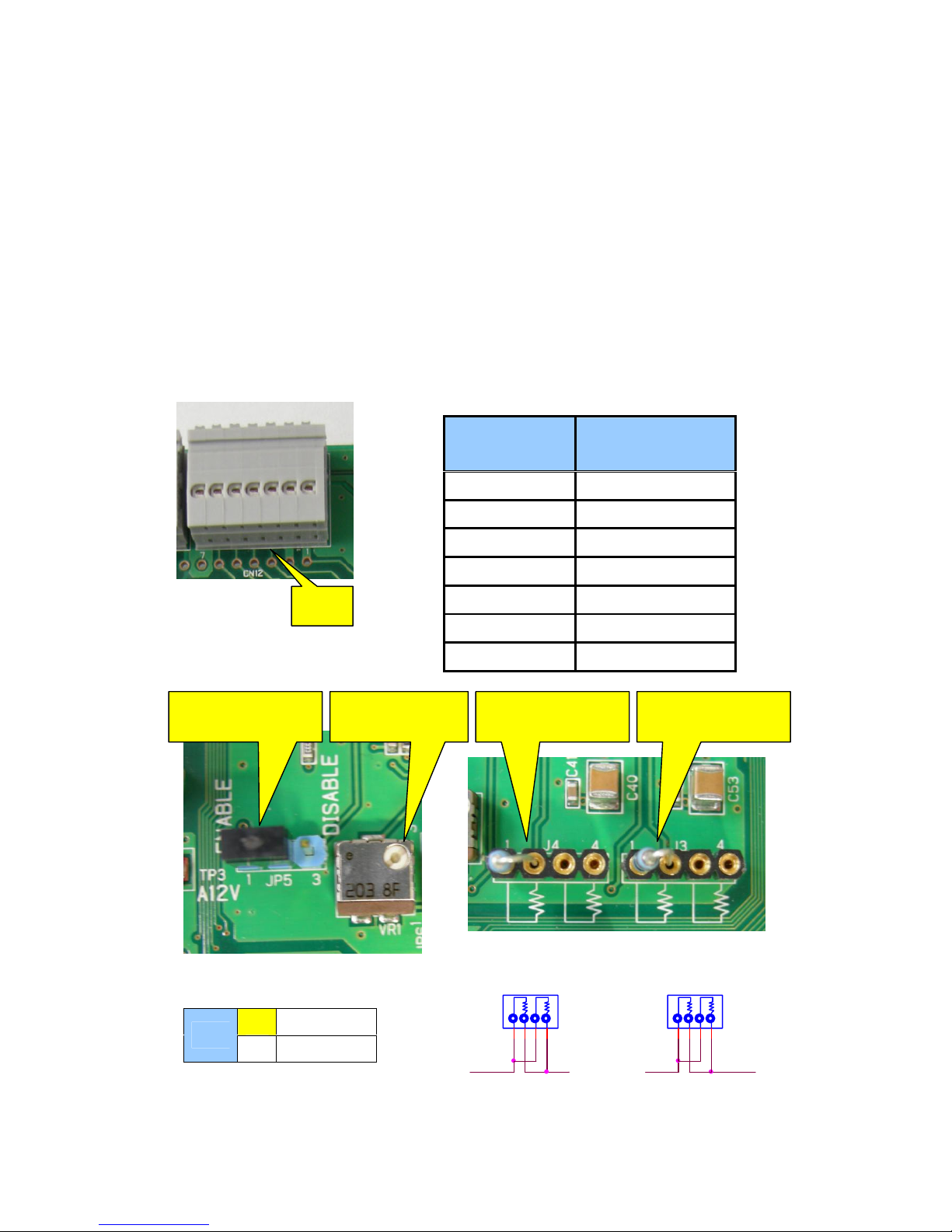
2.1 Resolver 1 I/O Connector (CN12)
This is the connector for excitation signals for resolver and SIN / COS signals for detection
coil.
Excitation signal outputs PWM signals through LPF (this can be set to disable. JP3) and
current AMP. It has variable resistance for level adjusting. Also, at the current AMP, it can
change the feedback adjusting resistance (J3,J4). As the default setting, the resistance is set
to 10kΩ. The feedback adjusting resistance can implement two parallel connections in one
socket.
The adjusting variable resistance (VR1) is a variable resistance of 20KΩ.
Connector Pin Signal Function
Number
1 Excitation Output +
2 Excitation Output -
3 SIN Input +
4 SIN Input -
5 COS Input +
CN12
6 COS Input -
7 AGND
The SIN, COS, and excitation signal of the detection coil are adjusted to the input level of the
microcomputer. It is connected to the microcomputer after noise canceling by LPF that is set
to Fc=234kHz for the level conversion and noise canceling purpose.
1-2 LPF Enable
JP5 2-3 LPF Disable
LPF Enable/Disable
Switch
Adjusting Variable
Resistance
Feedback Adjusting
Resistance
Feedback Adjusting
Resistance
J4
XR2C-3211-N(4pin)
3
4
1
2
J3
XR2C-3211-N(4pin)
3
4
1
2
- 6 -

For V850E2/PJ4-E, connections to CPU terminals are shown below.
Signals CPU Terminals
PWM Output P1_8/TPB0O/CSIG0SO/UARTH0TXD
Excitation Input + ADCA1I1/DFR10IM0
Excitation Input - DFR10IP0
SIN Input + ADCA1I2/DFR10IM1
SIN Input - DFR10IP1
COS Input - ADCA1I3/DFR10IM2
COS Input - DFR10IP2
- 7 -

2.2 Motor Control 1 Connector (CN14)
Motor Control 1 Connector is a connector to output digital signals for six-phase motor. It
connects six digital signals for UVW and one digital signal for gate block. The output is an open
drain output. It pulls up with 1KΩ for internal 5V.
Connector Signal Function
Pin Number
1 6-Phase PWM (Motor Control 1) U
2 6-Phase PWM (Motor Control 1) _U
3 6-Phase PWM (Motor Control 1) V
4 6-Phase PWM (Motor Control 1) _V
5 6-Phase PWM (Motor Control 1) W
6 6-Phase PWM (Motor Control 1) _W
CN14 7 Gate Block Output 1
8 DGND
Signals CPU Terminals
6-Phase PWM (Motor Control 1) U P1_1/TSG20O1
6-Phase PWM (Motor Control 1) _U P1_2/TSG20O2
6-Phase PWM (Motor Control 1) V P1_3/TSG20O3
6-Phase PWM (Motor Control 1) _V P1_4/TAUJ0O0/TSG20O4
6-Phase PWM (Motor Control 1) W P1_5/TAUJ0O1/TSG20O5
6-Phase PWM (Motor Control 1) _W P1_6/TAUJ0O2/TSG20O6
Gate Block Output 1 P4_2/UARTH2RTS/TSG20PTSI1/ENCA0E1/CSIG2SO
- 8 -
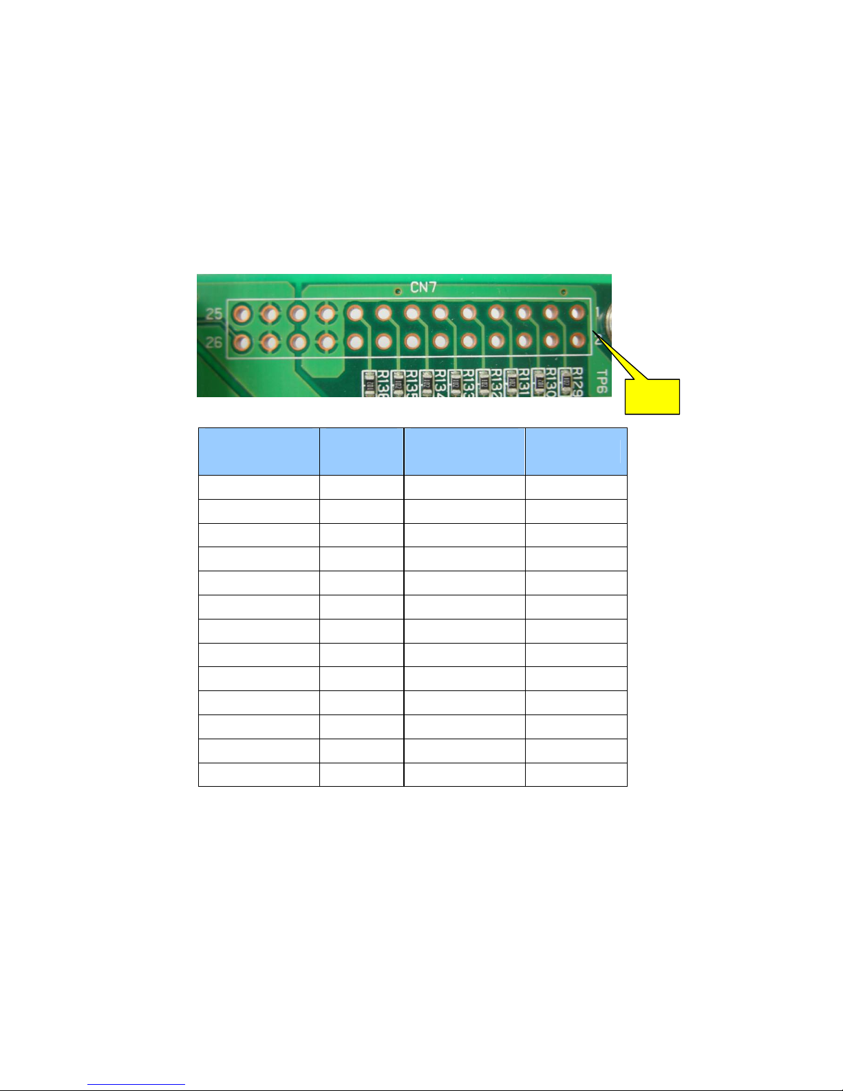
2.3 Analog Input Connector (CN7)
The Analog Input Connector is connected to CPU analog input terminal with adding protection
diode and resistance. The connector itself is not mounted, and it is 2.54pitch through-hole.
To use it for controlling, it has 1 digital input function. For some analog and digital signals, the
connection destination can be changed by JP settings.
CN7
Connector Pin Signal Connector Pin Signal Function
Number Function Number
1 A5V 2 A5V
3 ADCA0I1 4 ADCA0I2
5 ADCA0I3 6 ADCA0I4
7 AIN0 8 AIN1
9 ADCA0I14 10 ADCA0I15
11 ADCA0I16 12 ADCA0I17
13 ADCA0I18 14 ADCA0I19
15 ADCA0I20 16 ADCA0I21
17 ADCA0I22 18 ADCA0I8
19 AGND 20 AGND
21 NC 22 NC
23 DGND 24 DGND
25 DGND 26 Digital Input
- 9 -

Signals CPU Terminals
ADCA0I1 ADCA0I1
ADCA0I2 ADCA0I2
ADCA0I3 ADCA0I3
ADCA0I4 ADCA0I4
ADCA0I14 ADCA0I14
ADCA0I15 ADCA0I15
ADCA0I16 ADCA0I16
ADCA0I17 ADCA0I17
ADCA0I18 ADCA0I18
ADCA0I19 ADCA0I19
ADCA0I20 ADCA0I20
ADCA0I21 ADCA0I21
ADCA0I22 ADCA0I22
ADCA0I8 ADCA0I8
JP8:1-2 JP9:OPEN ADCA0I5
AIN0
JP8:2-3 JP9:SHORT ADCA0I10
JP12:1-2 JP13:OPEN ADCA0I6
AIN1 JP12:2-3 JP13:SHORT ADCA0I11
JP15:1-2 P0_5/TAUJ0I2/TAUJ0O2/UARTH2RXD/INTP2/CSIG0SI
Digital Input JP15:2-3 OPEN
JP13
JP9
JP15
JP12
JP8
- 10 -
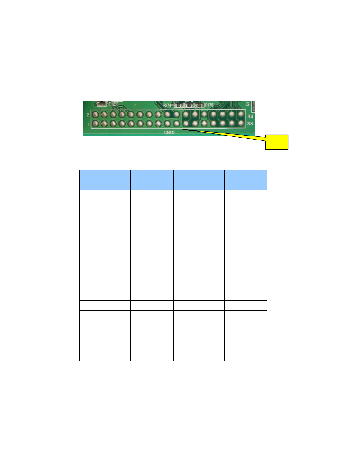
2.4 Digital I/O Connector (CN10)
The Digital I/O Connector is a connector with the functions for I/O of digital signals, UART
signals ( 5V level), and CAN communication. The connector itself is not mounted, and it is
2.54pitch through-hole.
CN10
Connector Pin Connector Pin
Signal Function Signal Function
Number Number
1 D5V 2 CN_RESO1
3 DGND 4 DGND
5 CN_LED1 6 CN_LED2
7 CN_LED3 8 CN_LED4
9 CN_LED5 10 CN_LED6
11 D5V 12 D5V
13 CN_CANH 14 CN_CANL
15 DGND 16 DGND
17 CN_UART0_TX 18 CN_UART0_RX
19 CN_UART1_TX 20 CN_UART1_RX
21 CN_BUSY0 22 CN_BUSY1
23 CN_RESETOUT 24 D5V
25 DGND 26 DGND
27 CN_SW1 28 CN_SW2
29 CN_SW3 30 CN_SW4
31 CN_SW5 32 CN_SW6
33 CN_ER1 34 CN_ER2
- 11 -
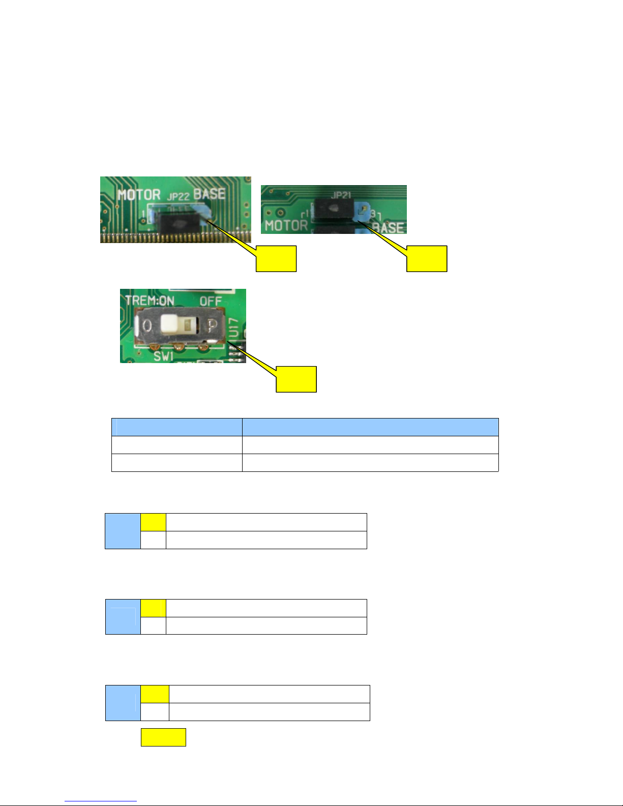
2.4.1 CAN
The communication signals from CPU board are connected to the connectors through CAN
transceiver.
It can be disconnected from the CAN transceiver on the motor board with JP setting. Also, the
termination resistance can be ON/OFF with SW
JP22 JP21
SW1
Signals CPU Terminals
transceiver TX P0_3/FCN0TX/UARTH0CTS/MODE1
transceiver RX P0_4/FCN0RX/UARTH0RTS
P0_3/FCN0TX/UARTH0CTS/MODE1 Connection Destination Settings
1-2 Connect to MOTOR Board Transceiver
JP21 2-3 Connect to BASE Board
P0_4/FCN0RX/UARTH0RTS Connection Destination Settings
1-2 Connect to MOTOR Board Transceiver
JP22
2-3 Connect to BASE Board
CAN Communication Line Termination Resistance Settings
ON Connect to Termination Resistance (120Ω)
SW1 OFF No Connection to Termination Resistance
Default
- 12 -

2.4.2 UART
The communication signals from CPU are connected to the connectors through buffer. The
output is an open drain output. It pulls up for internal power. It can be disconnected with jumper
setting.
Signals CPU Terminals
CN_UART0_TX P0_1/INTP4/ADCA0TRG1/CSIG0SO/UARTH0TXD/FCN1RX
CN_UART0_RX P0_0/INTP5/ADCA0TRG2/CSIG0SI/UARTH0RXD/INTP0/FCN1TX
CN_UART1_TX P3_1/TAUA1I3/TAUA1O3/TAUA1I2/TAUA1O2/UARTH1TXD/TAUA1O12
CN_UART1_RX P3_0/TAUA1I1/TAUA1O1/TAUA1I0/TAUA1O0/UARTH1RXD/INTP1/TAUA1O10
P0_1/INTP4 TXD/FCN1RX Connection Destination Settings
P0_0/INTP5/ADCA0TRG2/CSIG0SI/UARTH0RXD/INTP0/FCN1TX Connection Destination
Setti
P3_1/TAUA1I3/TAUA1O3/TAUA1I2/TAUA1O2/UARTH1TXD/TAUA1O12 Connection Destination
Settings
/ADCA0TRG1/CSIG0SO/UARTH0
ngs
1-2 Connect to MOTOR Board
JP23 2-3 Connect to BASE Board
1-2 Connect to MOTOR Board
JP24 2-3 Connect to BASE Board
1-2 Connect to MOTOR Board
JP25 2-3 Connect to BASE Board
JP23
JP24
JP25
JP26
- 13 -

P3_0/TAUA1I1/TAUA1O1/TAUA1I0/TAUA1O0/UARTH1RXD/INTP1/TAUA1O10 Connection
Destination S
ettings
1-2 Connect to MOTOR Board
JP26 2-3 Connect to BASE Board
- 14 -
2.4.3 Digital Output
The communication signals from CPU are connected to the connectors through buffer. The
output is an open drain output. It pulls up for internal power.
Signals CPU Terminals
CN_RESETOUT P6_0/CSIG2SI/TAUA0O12/TSG20O0/SIF0OE0
CN_LED1 P0_7/TAUJ0I0/TAUJ0O0/CSIG0SC
CN_LED2 P3_7/TAUA1I15/TAUA1O15/TAUA1I14/TAUA1O14/CSIG2RYI
CN_LED3 P4_1/UARTH2CTS/TSG20PTSI0/ENCA0E0/CSIG2SI
CN_LED4 P6_1/CSIG2SO/TAUA0O10/SIF0OE1
CN_LED5 P6_2/CSIG2SC/TAUA0O11//SIF0OE
CN_LED6 P7_7/TAUA0I14/TAUA0O14/TSG21O7/NMI/CSIH0CS7
- 15 -

2.4.4 Digital Input
The communication signals to CPU are connected through buffer. Some specific signals can be
disconnected with jumper setting. Also, the connections of CN_RESO1 can be selected.
JP20
JP24
Jumper
Signals CPU Terminals Settings
CN_SW1 1-2
P0_2/INTP3/ADCA0TRG0/CSIG0SC/UARTH0SC
CN_SW 2 3-4
P4_4/TAUJ0I0/UARTH1RTS/ESO0/INTP6/CSIG0RYO/CSIH0RYI/ADCA1TRG0
CN_SW 3 5-6
P6_3/UARTH1RXD/INTP1/TAUA1O10
CN_SW 4 7-8
P6_6/UARTH0RXD/INTP0/TAUA1O13
CN_SW 5 P6_7/UARTH0SC/TAUA1O14 9-10
JP20
CN_SW 6 11-12
P6_8/UARTH0TXD/TAUA1O15
CN_ER1 13-14
P4_6/TAUJ0I2/ADCA0CNV1/ESO2/INTP8/CSIH0SO/ADCA1TRG2/ADCA1CNV1
CN_ER2 15-16
P4_7/NMI/TAUJ0I3/ADCA0CNV0/ESO3/INTP9/ADCA1CNV0/CSIH0SC
CN_RESO1 JP18
P0_6/TAUJ0I1/TAUJ0O1/UARTH2TXD/CSIG0SO
CN_BUSY0 -
P6_4/UARTH1SC/TAUA1O11
CN_BUSY1 -
P6_5/UARTH1TXD/TAUA1O12
P0_6/TAUJ0I1/TAUJ0O1/UARTH2TXD/CSIG0SO Connection Destination Settings
1-2 Connect to MOTOR Board
JP18
2-3 Connect to BASE Board
- 16 -
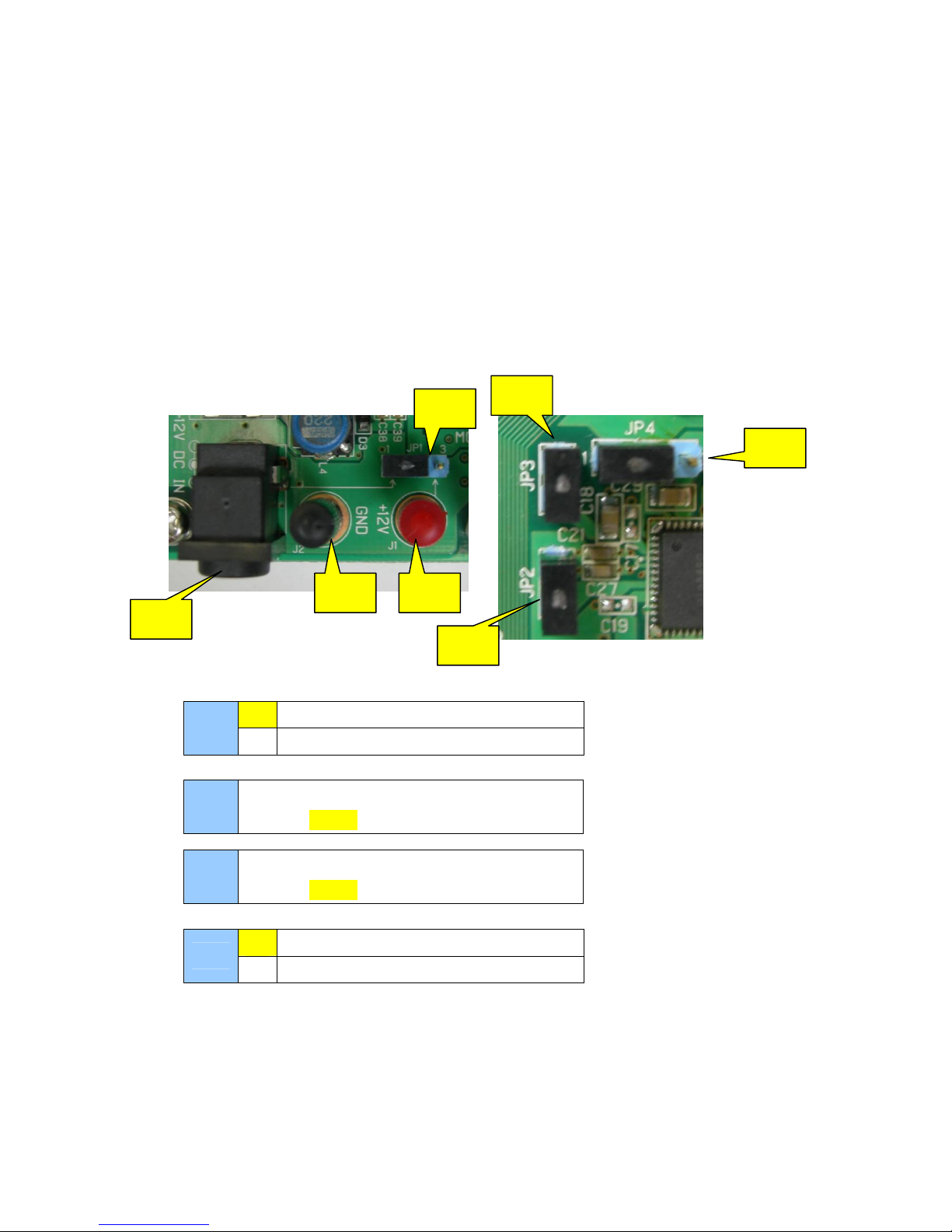
2.5 Power Supply
There are two ways to supply power. One is to supply power from AC JACK (CN4), another is to
supply power from the terminal. The power supply can be selected with JP1. The power voltage
is 12V. Also, there are jumpers for measuring current using on Motor board; D5V (JP2) for digital
and A5V (JP3) for analog.
JP4 is a jumper for controlling power when it is use as stand-alone. Do not change this normally.
Also, this board supplies power to CPU board and Base board when you use Motor board. In this
case, do not supply power to those boards directly.
1-2 Use AC JACK (CN4)
JP1 2-3 Use J1,J2 Terminals
JP2 Digital 5V Current Measurement
Normally, SHORT
JP3 Analog 5V Current Measurement
Normally, SHORT
1-2 When Using with CPU Board
JP4 2-3 When Stand-alone Use
JP3
JP1
JP4
J2 J1
CN4
JP2
- 17 -
Table of contents


