www.ti.com
Configuring the EVM
7
SLVUAS7A–July 2016–Revised February 2017
Submit Documentation Feedback Copyright © 2016–2017, Texas Instruments Incorporated
TPS25741EVM-802 and TPS25741AEVM-802 Evaluation Module User
Guide for Desktops
4 Configuring the EVM
4.1 Physical Access
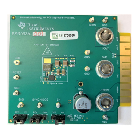
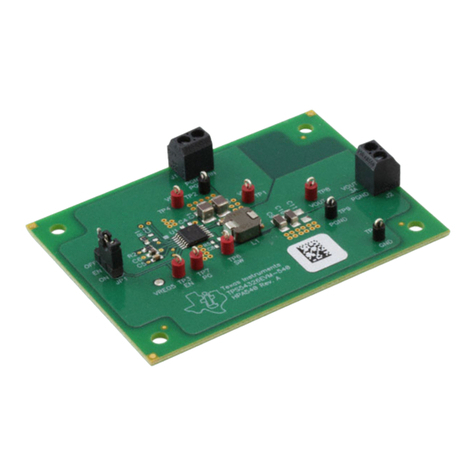
Table 2 lists the TPS25741EVM connector and functionality, Table 3 describes the default jumper
configuration, and Table 4 describes the test point availability.
Table 2. Connector and LED Functionality
Connector Label Description
J13 VIN Power bus input. Apply bus input voltage between J13 and J9.
J14 VBUS Output voltage that is applied to the VBUS of the USB Type-C cable. J14 along with J8 can
be used to apply an external load.
J9, J8 GND Power bus input return connector
J11 J11 Barrel jack input from an AC to DC power supply
J12 J12 USB Type-C receptacle
D9 VIN This Green LED indicates input power supply
D12, D5 DCDC_5V,
DCDC_2 The two Green LEDs indicate whether upstream DCDCs are on
D2, D3, D4 AUDIO
DEBUG
POL
D2 indicates when the AUDIO accessary adaptor is inserted
D3 indicates when the DEBUG accessary adaptor is inserted
D4 indicates when the UFP is inserted on positive orientation
D13, D11, D10 5 V
9 V/12 V
15 V/20 V
D13 indicates when output voltage is 5 V
D11 indicates when output voltage is 9 V or 12 V
D10 indicates when output voltage is 15 V or 20 V
Table 3. Jumper Functionality
Jumper Label Description
J4 PSEL/PCTRL Used to program the PSEL and PCTRL pins of the TPS25741 and TPS25741A. This advertises
the power level to the UFP. Install a single shunt in the P1, P2, P3, or P4 position. Optionally, a
second shunt can be installed in the PCTRL position. The position locations are shown in
Figure 5 and also on the PCB silk screen near J4.
P1 position: PSEL = 93 W
P2 position (default): PSEL = 65 W
P3 position: PSEL = 45 W
P4 position: PSEL = 36 W
PCTRL position (shunt installed): PMAX = PSEL/2
PCTRL position (no shunt installed-default): PMAX = PSEL
J3 HIPWR/ENMV Used to program the HIPWR and EN12V/EN9V pins of the TPS25741 and TPS25741A. This
advertises maximum voltage and maximum current to the UFP. Install a single shunt in the H1,
H2, H3, or H4 position. Optionally, a second shunt can be installed in the EN12V position. The
position locations are shown in Figure 4 and also on the PCB silk screen near J3. V1 = 5 V, V2 =
9 V or 12 V, V3 = 15 V or 20 V
EN12V or EN9V = HIGH (no shunt installed-default) => V1 and V2
EN12V or EN9V = LOW (shunt installed) => No V2
H1 position: V3 and IMAX = 5 A (OCP = 6.3 A)
H2 position: => V3 and IMAX = 3 A (OCP = 4.2 A)
H3 position: No V3 and IMAX = 5 A (OCP = 6.3 A)
H4 position (default): No V3 and IMAX = 3 A (OCP = 4.2 A)
Advertised current at Vx => Ix = min(PMAX/Vx, IMAX)
J16 V_Cable Used to disconnect D2, D3, D4
J18 V_LED Used to disconnect D10, D11, D13
J15 BC 1.2 Used to enable or disable the BC1.2 function
J5 VPWR Used to select power source for VPWR
J6 VPDD Used to select power source for VDD
J10, J7 CC1, CC2 Used to put Ra or Rd to CC lines
J1, J17 Used to connect two EVMs together to enable PPM
J2 Used to enable two EVMs to share a single power supply when doing PPM
