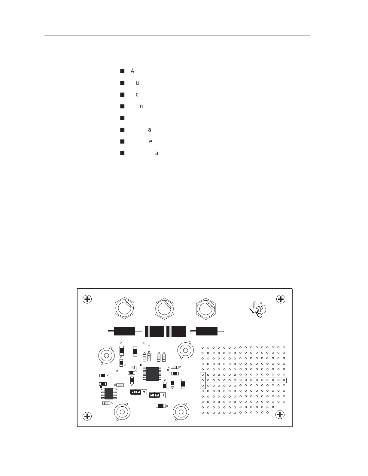
Texas ths6022 User manual

THS6022 250ĆmA
Dual Differential Drivers
Evaluation Module
November 1998 Mixed-Signal Products
User’s Guide
SLOU035

IMPORTANT NOTICE
TexasInstruments andits subsidiaries(TI) reservethe rightto makechanges totheir productsor todiscontinue
any product or service without notice, and advise customers to obtain the latest version of relevant information
to verify, before placing orders, that information being relied on is current and complete. All products are sold
subject to the terms and conditions of sale supplied at the time of order acknowledgement, including those
pertaining to warranty, patent infringement, and limitation of liability.
TI warrants performance of its semiconductor products to the specifications applicable at the time of sale in
accordance with TI’s standard warranty. Testing and other quality control techniques are utilized to the extent
TIdeemsnecessarytosupport thiswarranty.Specific testingofall parametersofeachdeviceis notnecessarily
performed, except those mandated by government requirements.
CERTAIN APPLICATIONS USING SEMICONDUCTOR PRODUCTS MAY INVOLVE POTENTIAL RISKS OF
DEATH, PERSONAL INJURY, OR SEVERE PROPERTY OR ENVIRONMENTAL DAMAGE (“CRITICAL
APPLICATIONS”). TI SEMICONDUCTOR PRODUCTS ARE NOT DESIGNED, AUTHORIZED, OR
WARRANTED TO BE SUITABLE FOR USE IN LIFE-SUPPORT DEVICES OR SYSTEMS OR OTHER
CRITICALAPPLICATIONS.INCLUSIONOFTIPRODUCTSINSUCHAPPLICATIONSISUNDERSTOODTO
BE FULLY AT THE CUSTOMER’S RISK.
In order to minimize risks associated with the customer’s applications, adequate design and operating
safeguards must be provided by the customer to minimize inherent or procedural hazards.
TIassumes noliabilityforapplicationsassistance orcustomer productdesign. TIdoes notwarrantorrepresent
thatanylicense,eitherexpressorimplied,isgrantedunderanypatentright,copyright,maskworkright,orother
intellectual property right of TI covering or relating to any combination, machine, or process in which such
semiconductor products or services might be or are used. TI’s publication of information regarding any third
party’s products or services does not constitute TI’s approval, warranty or endorsement thereof.
Copyright 1998, Texas Instruments Incorporated

iii
Chapter Title—Attribute Reference
Preface
Related Documentation From Texas Instruments
J
THS6022 250-mA DUAL DIFFERENTIAL DRIVERS
(literature
numberSLOS225). This isthedatasheet for theTHS6022 amplifier
integrated circuit used on the EVM
J
THS4001 HIGH-SPEED LOW-POWER OPERATIONAL
AMPLIFIER
(literature number SLOS206) This is the data sheet
for the THS4001 amplifier integrated circuit used on the EVM.
J
PowerPAD
Thermally Enhanced Package
(literature number
SLMA002) This is the technical brief for the special PowerPAD
package in which the THS6022 amplifier IC is supplied.
FCC Warning
This equipment is intended for use in a laboratory test environment only. It
generates, uses, and can radiate radio frequency energy and has not been
testedforcompliancewiththelimitsofcomputing devices pursuant to subpart
Jofpart 15ofFCCrules,which aredesignedtoprovidereasonableprotection
against radio frequency interference. Operation of this equipment in other
environments may cause interference with radio communications, in which
case the user at his own expense will be required to take whatever measures
may be required to correct this interference.
Trademarks
TI is a trademark of Texas Instruments Incorporated.

iv

Running Title—Attribute Reference
v
Chapter Title—Attribute Reference
Contents
1 General Information 1-1. . . . . . . . . . . . . . . . . . . . . . . . . . . . . . . . . . . . . . . . . . . . . . . . . . . . . . . . . . . . .
1.1 Features 1-2. . . . . . . . . . . . . . . . . . . . . . . . . . . . . . . . . . . . . . . . . . . . . . . . . . . . . . . . . . . . . . . . . .
1.2 Description 1-2. . . . . . . . . . . . . . . . . . . . . . . . . . . . . . . . . . . . . . . . . . . . . . . . . . . . . . . . . . . . . . . .
1.3 Input Configuration 1-5. . . . . . . . . . . . . . . . . . . . . . . . . . . . . . . . . . . . . . . . . . . . . . . . . . . . . . . . .
1.4 THS6022 EVM Specifications 1-5. . . . . . . . . . . . . . . . . . . . . . . . . . . . . . . . . . . . . . . . . . . . . . . .
1.5 Using The THS6022 EVM 1-6. . . . . . . . . . . . . . . . . . . . . . . . . . . . . . . . . . . . . . . . . . . . . . . . . . .
1.6 THS6022 EVM Performance 1-7. . . . . . . . . . . . . . . . . . . . . . . . . . . . . . . . . . . . . . . . . . . . . . . . .
1.7 General High-Speed Amplifier Design Considerations 1-8. . . . . . . . . . . . . . . . . . . . . . . . . . .
1.8 General PowerPAD Design Considerations 1-9. . . . . . . . . . . . . . . . . . . . . . . . . . . . . . . . . . . .
2 Reference 2-1. . . . . . . . . . . . . . . . . . . . . . . . . . . . . . . . . . . . . . . . . . . . . . . . . . . . . . . . . . . . . . . . . . . . . . .
2.1 THS6022 Dual Differential Line Drivers EVM Parts List 2-2. . . . . . . . . . . . . . . . . . . . . . . . . .
2.2 THS6022 EVM Board Layouts 2-3. . . . . . . . . . . . . . . . . . . . . . . . . . . . . . . . . . . . . . . . . . . . . . . .

Running Title—Attribute Reference
vi
Figures
1–1 THS6022 Evaluation Module 1-2. . . . . . . . . . . . . . . . . . . . . . . . . . . . . . . . . . . . . . . . . . . . . . . . . . .
1–2 THS6022 Evaluation Module Schematic 1-3. . . . . . . . . . . . . . . . . . . . . . . . . . . . . . . . . . . . . . . . .
1–3 THS6022 Evaluation Module Block Diagram 1-5. . . . . . . . . . . . . . . . . . . . . . . . . . . . . . . . . . . . . .
1–4 THS6022 EVM Driver Frequency Response With a 50-W Load 1-7. . . . . . . . . . . . . . . . . . . . .
1–5 THS6022 EVM Driver Frequency Response Test Circuit 1-7. . . . . . . . . . . . . . . . . . . . . . . . . . . .
1–6 PowerPAD PCB Etch and Via Pattern – Minimum Requirements 1-9. . . . . . . . . . . . . . . . . . . .
1–7 Maximum Power Dissipation vs. Free-Air Temperature 1-10. . . . . . . . . . . . . . . . . . . . . . . . . . . .
2–1 THS6022 EVM Component Placement Silkscreen and Layout 2-3. . . . . . . . . . . . . . . . . . . . . .
2–2 THS6022 EVM PC Board: Layer 1 — Top Side Layout 2-3. . . . . . . . . . . . . . . . . . . . . . . . . . . . .
2–3 THS6022 EVM PC Board: Layer 2 — Back Side Ground Plane Layer 2-4. . . . . . . . . . . . . . . .
2–4 THS6022 EVM PC Board: Solder Mask — Back Side 2-4. . . . . . . . . . . . . . . . . . . . . . . . . . . . . .

1-1
General Information
General Information
This chapter details the Texas Instruments (TI) THS6022 250-mA Dual
Differential Line Driver Evaluation Module (EVM), SLOP133. It includes a list
ofEVMfeatures,abriefdescriptionofthemoduleillustratedwithapictorialand
schematic diagrams, EVM specifications, details on configuring, connecting,
and using the EVM, and a discussion on high-speed amplifier and PowerPAD
package design considerations.
Topic Page
1.1 Features 1–2. . . . . . . . . . . . . . . . . . . . . . . . . . . . . . . . . . . . . . . . . . . . . . . . . . . . .
1.2 Description 1–2. . . . . . . . . . . . . . . . . . . . . . . . . . . . . . . . . . . . . . . . . . . . . . . . . . .
1.3 Input Configuration 1–5. . . . . . . . . . . . . . . . . . . . . . . . . . . . . . . . . . . . . . . . . . .
1.4 THS6022 EVM Specifications 1–5. . . . . . . . . . . . . . . . . . . . . . . . . . . . . . . . . . .
1.5 Using The THS6022 EVM 1–6. . . . . . . . . . . . . . . . . . . . . . . . . . . . . . . . . . . . . .
1.6 THS6022 EVM Performance 1–7. . . . . . . . . . . . . . . . . . . . . . . . . . . . . . . . . . . .
1.7 General High-Speed Amplifier Design Considerations 1–9. . . . . . . . . . .
1.8 General PowerPADDesign Considerations 1–10. . . . . . . . . . . . . . . . . .
Chapter 1

Features
1-2
General Information
1.1 Features
THS6022 250-mA Dual Differential Driver EVM features include:
J
A Complete Client Side ADSL Differential Line Driver
J
Multiple Input Configurations Set Via On Board Jumpers
J
Includes a THS4001 High-Speed Amplifier as an Inverter
J
Standard BNC Connectors Inputs and Outputs
J
±5-V to ±15-V Operation
J
Nominal 50-ΩImpedance Inputs
J
Pad Area On Board For User Component Placement and Testing
J
Good Example of PowerPAD Package and High-Speed Amplifier
Design and Layout
1.2 Description
The TI THS6022 250-mA Dual Differential Line Driver Evaluation Module
(EVM) is a complete client side ADSL high-speed driver circuit. It consists of
the TI THS6022 Dual Differential Line Driver IC, a TI THS4001 High-Speed
Low-Power Operational Amplifier IC, and a number of passive parts, all
mounted on a multilayer circuit board (Figure 1–1). The EVM uses standard
BNC connectors for inputs and outputs and also includes a pad area for user
component connection and testing. It is completely assembled, fully tested,
and ready to use — just connect it to power, a signal source, and a load
(if desired).
Figure 1–1.THS6022 Evaluation Module
J2
+VCC GND
J1
+
C8
U1
+Driver 1 Output
L2 Texas Instruments
THS6022 EVM
SLOP133
Rev. B
–VCC
J3
Driver 1
Input J4
R5
R6
L1 C1
R1
R2
J5
U2
R3
JP2
C10
R12
Driver 2 Output
Pad1
GND
Pad2
C3
R4
C7
Driver 2
Input J6
JP1
R9
R10
J7
C5
R8
C2
C13 C14
C9
R13
R15

Description
1-3
General Information
Inputpowerisappliedto the EVM through banana jacks J1,J2,andJ3.AnLC
filteroneachpowerbusisolatestheEVMcircuitsfromtheexternalsupply.The
schematic for the EVM appears in Figure 1–2.
Figure 1–2.THS6022 Evaluation Module Schematic
1
–
+
U2:A
THS6022
2
1
3
5
4
R4
1 KΩ
R2
49.9 Ω
R3
1 KΩ
R1
49.9 Ω
R8
49.9 Ω
R7
TBD
15 V
–15 V
R5
1 KΩ
15 V
–
+6
4
7
–15 V
2
3
JP1
JP2
R9
49.9 Ω
–
+13
14
12
10
11
R11
TBD
U2:B
THS6022
–15 V
R15
49.9 Ω
R14
TBD
R12
1 KΩ
R13
1 KΩ
C4
TBD
C13
0.1 µF
C3
0.1 µF
C2
0.1 µF
C6
TBD
R6
1 KΩ
U1
THS4001
C7
0.1 µF
C5
0.1 µF
C12
TBD
C10
0.1 µF
C9
0.1 µF
C14
0.1 µF
C11
TBD
J4
Driver 1
Input
1
J6
Driver 2
Input
R10
49.9 Ω
15 V
J5
Driver 1
Output
Driver 2
Output
J7
GND
2 OUT
1 OUTPad1
Pad2
L2
0.22 µH
C8
6.8 µF
J3
C1
6.8 µF
L1
0.22 µH
–15 V
J1
15 V
J2

Description
1-4
General Information
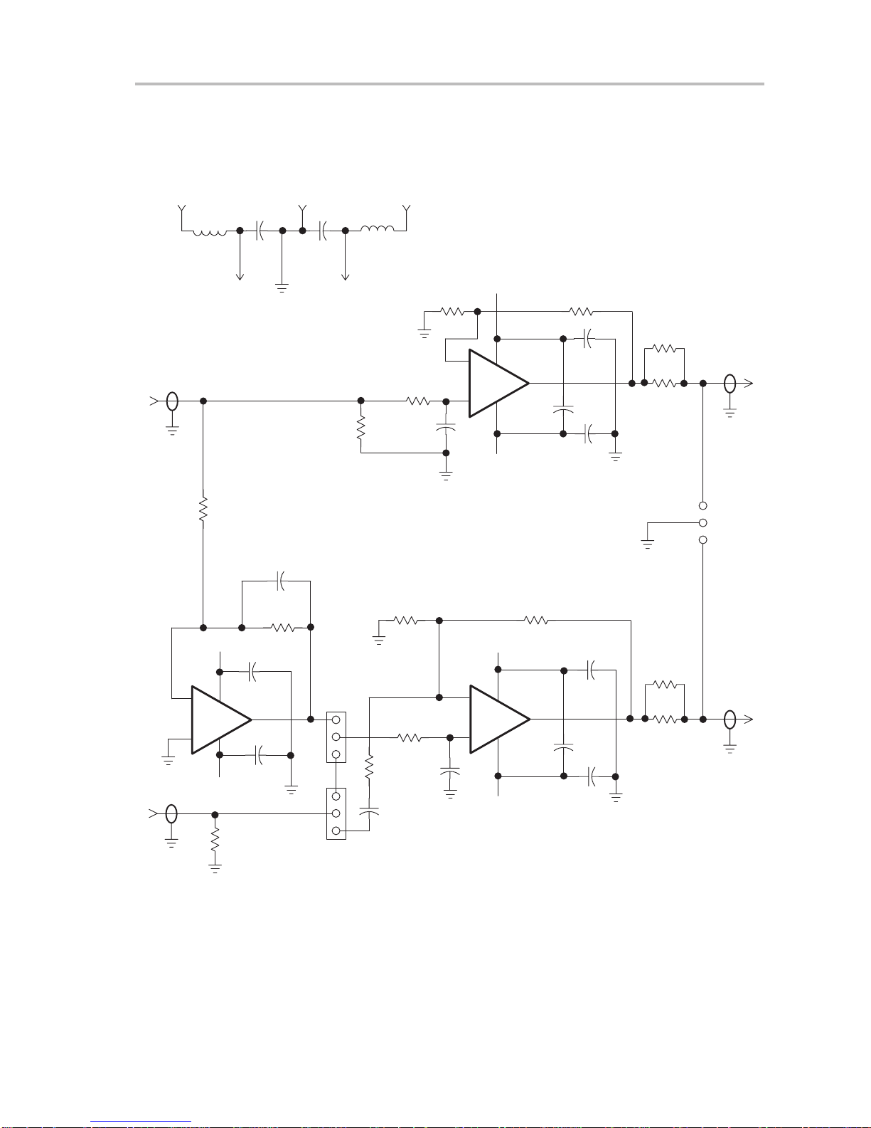
The THS6022 EVM is equipped with a separate BNC connector for the Driver
1 input and the Driver 2 input. Each input is terminated with a 50-Ωresistor to
provide correct line impedance matching (Figure 1–2). Note that using a
source with a 50-Ωoutput impedance will create a voltage divider at the EVM
inputs. Thus, accurate knowledge of the source output characteristics is
required to determine proper input signal amplitudes.
Driver outputs are routed through client side ADSL-standard 49.9-Ωresistors
to provide correct transmission line impedance matching when run through a
1:1 transformer with a 100-Ωline termination. These resistors also allow
separatereceiverstoviewadifferentialinputsignalfromthetransmissionline.
All of the amplifiers on the EVM (THS6022 and THS4001) follow the classic
operational amplifier gain equations:
Inverting Gain
+
–RF
RG(1)
Non-Inverting Gain
+
1
)
RF
RG(2)
The gain of the amplifiers can be easily changed to support different
applications by changing resistor ratios. Any of the components on the EVM
boardcanbe replacedwithdifferentvalues.Also,componentpadshave been
placed in convenient locations on the PCB (shown as components with the
valueTBDintheschematic)toallownumerousmodificationstothebasicEVM
configuration. However, care must be taken because the surface-mount
solder pads on the board are somewhat fragile and will not survive a large
number of soldering/desoldering operations.
The THS6022 IC is a current-feedback amplifier (CFB) and because of this,
extracaremustbe taken to ensure thatafeedbackresistoris always included
in the design. In addition, there must never be a capacitor directly in the
feedback path between the noninverting input and the amplifier output.
Disregarding this guideline will likely result in a part that oscillates. The
THS4001 IC amplifier used on the EVM, however, is a classic
voltage-feedback amplifier (VFB) and has no restrictions on resistors or
capacitors in the feedback path. But, to maximize bandwidth, high value
resistors and capacitors should be used with discretion.
Andfinally,theEVMcircuitboardisagood example of proper boardlayoutfor
high-speed amplifier and PowerPAD designs. It can be used as a guide for
user application layouts.

Input Configuration
1-5
General Information
1.3 Input Configuration
The THS6022 EVM inputs can be configured in several different ways to
provide a wide variety of circuits to support different applications
(Figure 1–3). Each of the two jumpers on the EVM is a three-pin header that
is used as a SPDT switch by placing a shunt across two pins to select either
of two possible signal routes.
Figure 1–3.THS6022 Evaluation Module Block Diagram
J4
1
3
2
JP1
1
32
JP2
–
+
J6
THS6022
THS6022
THS4001
U1
U2: A
U2: B
Driver 1 Output
Driver 2 Output
Driver 1
Input
Driver 2
Input
Positive Driver
Inverter
Negative Driver
J5
J7
-
Jumper JP1:
J
1–2 — connects the noninverting input of driver 2 (U2: B) to the
THS4001 inverting amplifier (U1) output
J
2–3 — connects the noninverting input of driver 2 (U2: B) to the input
connector (J6) when jumper JP2 is set appropriately
-
Jumper JP2:
J
1–2 — connects the driver 2 input connector (J6) to the noninverting
input of driver 2 (U2:B) when jumper JP1 is set appropriately
J
2–3—connectsthedriver 2 inputconnector(J6)totheinvertinginput
of driver 2 (U2:B) when jumper JP1 is set appropriately
Forexample,touseasingle-endedinput,jumperJP1shouldbesetto1–2and
the input signal applied to input connector J4. The output of the THS6022
driversisadifferentialsignaldueto theinverter(U1)andJP1 beingsetto1–2.
For a differential source, JP1 should be set to 2–3, JP2 should be set to 1–2
and the differential input signal applied between input connectors J4 and J6.
If JP2 is in the 2–3 position, components C12 and R11 must be installed, R9
must be removed, and a 0-Ωresistor must be installed in the C11 position for
proper operation.
1.4 THS6022 EVM Specifications
Supply voltage range, ±VCC ±5 V to ±15 V. . . . . . . . . . . . . . . . . . . . . . . . . . . . . . . . . . . . . . . . . . . .
Supply current, ICC 23 mA. . . . . . . . . . . . . . . . . . . . . . . . . . . . . . . . . . . . . . . . . . . . . . . . . . . . . . . . . . .
Input voltage, VI±VCC, max. . . . . . . . . . . . . . . . . . . . . . . . . . . . . . . . . . . . . . . . . . . . . . . . . . . . . . . . .
Output drive, THS6022 Drivers, IO250 mA, typ each. . . . . . . . . . . . . . . . . . . . . . . . . . . . . . . . . . . .
Continuous total power dissipation at TA = 25°C (THS6022), 3.3 W, max. . . . . . . . . . . . . . . . . . .
For complete THS6022 amplifier IC specifications and parameter
measurement information, and additional application information, see the
THS6022 data sheet, TI Literature Number SLOS225.

Using The THS6022 EVM
1-6
General Information
1.5 Using The THS6022 EVM
The THS6022 EVM operates from a split power supply with voltages ranging
from ±5 V to ±15 V. The use of a single supply for this EVM is not
recommended. As shipped, the output of driver 1 is equal to a noninverting
gain of 2 when using the single-ended input mode. The output of driver 2 is
equal to an inverting gain of 2 under the same conditions. An oscilloscope is
typically used to view and analyze the EVM output signals.
1) Ensurethatallpowersuppliesaresetto
OFF
beforemakingpowersupply
connections to the THS6022 EVM.
2) Select the operating voltage for the EVM and connect appropriate split
powersuppliestothebanana jacks on the module marked
+V
CC
(J1)and
–V
CC
(J3)
.
3) Connect the power supply ground to the module banana jack marked
GND
(J2).
4) Connect an oscilloscope to U2, pin2. This is the driver 1 amplifier output.
Connecting directly to the DRIVER 1 OUTPUT BNC connector (J5) with
a50-Ωnominalimpedancecableandanoscilloscopehavinga50-Ωinput
termination is preferred for examining very high frequency
signals.
5) Set jumper J1 to the 1–2 position.
6) Set jumper J2 to the 1–2 position.
7) Set the power supply to
ON
8) Connect a signal input to the DRIVER 1 INPUT BNC (J4).
EachinputconnectoronthisEVMisterminatedwitha50-Ωresistortoground.
With a 50-Ωsource impedance, the voltage seen by the THS6022 amplifier
IC on the EVM will be 1/2 the source signal voltage applied to the EVM input
connector.
9) Verifytheoutputsignalontheoscilloscope.Withahigh-impedancescope
probe, the output signal should be twice the source amplitude. Using the
50-Ωinput impedance of an oscilloscope will show 1/2 the actual
THS6022 amplifier IC output voltage. This is due to the voltage division
between the source resistance and the oscilloscope 50-Ωinput
impedance. When connected to J7 (Driver 2 output), the signal should be
180°phase shifted from the Driver 1 output (J5).

THS6022 EVM Performance
1-7
General Information
1.6 THS6022 EVM Performance
Figure1–4showsthetypicalfrequencyresponseoftheTHS6022EVMdrivers
whenproperlyloaded.Thisdatawascollectedusingasingle-endedinputwith
a100-Ωloadconnectedbetweenthedriveroutputs,asshowninthetestcircuit
of Figure 1–5.
Typical–3-dBbandwidthwitha±15Vpowersupplyis70MHzfordriver2and
60 MHz for driver 1. With a ±5 V power supply, typical –3-dB bandwidth is
75 MHzfordriver2and70MHzfordriver1.Thedifferencebetweentheoutput
signals of driver 1 and driver 2 is primarily due to the high-frequency
characteristics of the inverting amplifier (U1). Component values can be
changed to cause the two responses to track more closely, but since ADSL
signals are limited to 2 MHz and below, the high-frequency imbalance can
usually be ignored.
Figure 1–4.THS6022 EVM Driver Frequency Response With a 50-
Ω
Load
f – Frequency – Hz
OUTPUT LEVEL
vs
FREQUENCY
–1
–3 10M100k
1
3
500M
Output Level – dB
5
7
1M 100M
VCC = ±5V
VI(PP) = 2 V
RL= 200 ΩDifferential
JP1 : 1–2
JP2 : 1–2 Driver 1
Driver 2
0
–2
2
4
6
f – Frequency – Hz
OUTPUT LEVEL
vs
FREQUENCY
–1
–3 10M100k
1
3
500M
Output Level – dB
5
7
1M 100M
VCC = ±15V
VI(PP) = 2 V
RL= 200 ΩDifferential
JP1 : 1–2
JP2 : 1–2
Driver 1
0
–2
2
4
6
Driver 2
Figure 1–5.THS6022 EVM Driver Frequency Response Test Circuit
RL
100 Ω
Driver 2 Output
2 OUT
Pad 2
1 OUT
Pad 1
GND
Driver 1 Output J5
J7
User Pad Area
R8
49.9 Ω
R15
49.9 Ω

General High-Speed Amplifier Design Considerations
1-8
General Information
1.7 General High-Speed Amplifier Design Considerations
The THS6022 EVM layout has been designed and optimized for use with
high-speedsignalsandcanbeusedasanexamplewhendesigningTHS6022
applications. Careful attention has been given to component selection,
grounding,powersupplybypassing,andsignalpathlayout.Disregardofthese
basic design considerations could result in less than optimum performance of
the THS6022 250-mA dual differential line driver IC.
Surface-mountcomponents were selectedbecause of the extremelylow lead
inductance associated with this technology. Also, because surface-mount
components are physically small, the layout can be very compact. This helps
minimize both stray inductance and capacitance.
Tantalumpowersupplybypasscapacitors(C1andC8)atthepowerinputpads
helpsupplycurrentsforrapid,largesignalchangesattheamplifieroutput.The
0.1 µF power supply bypass capacitors (C2, C3, C5, and C7) were placed as
close as possible to the IC power input pins in order to keep the PCB trace
inductance to a minimum. This improves high-frequency bypassing and
reducesharmonicdistortion.Additional0.1µFcapacitors(C13andC14)were
placedbetween+VCC and–VCC. This helpsminimizetheharmonicdistortion
of the amplifiers.
A proper ground plane should always be used with high-speed circuit design.
This provides low-inductive ground connections for return current paths.
Special attention is needed for the inverting input pins. Stray capacitance at
these pins can seriously degrade the performance of the amplifiers. In
addition, ground plane coupling into these pins can cause noise to appear at
the outputs of the amplifiers. This is especially important for the inverting pin
whilethe amplifier is operatinginthe noninverting mode. Becausethe voltage
at this pin swings directly with the noninverting input voltage, any stray
capacitance would allow currents to flow into the ground plane, causing
possible gain error and/or oscillation. Capacitance variations at the amplifier
IC input pin of less than 1 pF can significantly affect the response of the
amplifier.
In general, it is always best to keep signal lines as short and as straight as
possible. Sharp 90
_
corners should generally be avoided — round corners or
a series of 45
_
bends should be used, instead. Stripline techniques should
also be incorporated when signal lines are greater than 3 inches in length.
These traces should be designed with a characteristic impedance of either
50 Ωor 75 Ω, as required by the application. Such signal lines should also be
properly terminated with an appropriate resistor.
Finally,properterminationofallinputsandoutputsshouldbeincorporatedinto
the layout. Unterminated lines, such as coaxial cable, can appear to be a
reactive load to the amplifier IC. By terminating a transmission line with its
characteristic impedance, the amplifier’s load then appears to be purely
resistive, and reflections are absorbed at each end of the line. Another
advantage of using an output termination resistor is that capacitive loads are
isolated from the amplifier output. This isolation helps minimize the reduction
in amplifier phase-margin and improves the amplifier stability for improved
performance such as reduced peaking and settling times.

General PowerPAD Design Considerations
1-9
General Information
1.8 General PowerPAD Design Considerations
TheTHS6022ICismountedinaspecial package incorporating a thermalpad
thattransfersheatfromtheICdiedirectlytothePCB.ThePowerPADpackage
is constructed using a downset leadframe. The die is mounted on the
leadframe but is electrically isolated from it. The bottom surface of the lead
frameisexposedasametalthermalpad on the underside of the package and
makes physical contact with the PCB. Because this thermal pad is in direct
physicalcontactwithboththedieandthePCB,excellentthermalperformance
can be achieved by providing a good thermal path away from the thermal pad
mounting point on the PCB.
Although there are many ways to properly heatsink this device, the following
steps illustrate the recommended approach as used on the THS6022 EVM,
which is built on a multilayer PCB with an internal ground plane.
1) Prepare the PCB with a top side etch pattern as shown in Figure 1–6.
There should be etch for the leads as well as etch for the thermal pad.
Figure 1–6.PowerPAD PCB Etch and Via Pattern – Minimum Requirements
Thermal pad area (0.15 x 0.17) with 6 vias
(Via diameter = 13 mils)
2) Place6holesintheareaofthethermalpad.Theseholesshouldbe13mils
in diameter. They are kept small so that solder wicking through the holes
is not a problem during reflow.
3) Additional vias may be placed anywhere along the thermal plane outside
of the thermal pad area. This will help dissipate the heat generated from
the THS6022. These additional vias may be larger than the 13 mil diame-
ter vias directly under the thermal pad. They can be larger because they
arenotinthethermal-padareatobesoldered,therefore,wickingisgener-
ally not a problem.
4) Connect all holes to the internal ground plane.
5) Whenconnectingtheseholestothegroundplane,DONOTusethetypical
web or spoke via connection methodology. Web connections have a high
thermal resistance connection that is useful for slowing the heat transfer
during soldering operations. This makes the soldering of vias that have
plane connections easier. However, in this application, low thermal
resistance is desired for the most efficient heat transfer. Therefore, the
holes under the THS6022 package should make their connection to the
internal ground plane with a complete connection around the entire
circumference of the plated through hole.
6) The top-side solder mask should leave exposed the terminals of the
packageandthethermalpadareawithits6holes.Thebottom-sidesolder
maskshouldcoverthe6holesofthethermalpadarea.Thiseliminatesthe
solderfrombeingpulledawayfromthethermalpad areaduringthereflow
process.

General PowerPAD Design Considerations
1-10
General Information
7) Apply solder paste to the exposed thermal pad area and all of the
operational amplifier terminals.
8) With these preparatory steps in place, the THS6022 is simply placed in
position and run through the solder reflow operation as any standard
surface-mount component. This results in a part that is properly installed.
The actual thermal performance achieved with the THS6022 in its PowerPAD
package depends on the application. In the example above, if the size of the
internal ground plane is approximately 3 inches ×3 inches, then the expected
thermal coefficient, θJA,is about 37.5
_
C/W. For a given θJA, the maximum
power dissipation is shown in Figure 1–7 and is calculated by the following
formula:
PD
+ǒ
TMAX–TA
q
JA
Ǔ
Where: PD= Maximum power dissipation of THS6022 (watts)
TMAX= Absolute maximum junction temperature (150°C)
TA= Free-ambient air temperature (°C)
θJA = θJC + θCA
θJC = Thermal coefficient from junction to case (2.07°C/W)
θCA = Thermal coefficient from case to ambient air
Figure 1–7.Maximum Power Dissipation vs. Free-Air Temperature
TA– Free-Air Temperature – °C
–40 –20 0 20 80 1006040
MAXIMUM POWER DISSIPATION
vs
FREE-AIR TEMPERATURE
5
3
1
0
4
2
6
Maximum Power Dissipation – W
Tj= 150°C
PCB Size = 3” x 3”
No Air Flow
θJA = 37.5°C/W
2 oz Trace and
Copper Pad
with Solder
θJA = 97.7°C/W
2 oz Trace and Copper Pad
without Solder

General PowerPAD Design Considerations
1-11
General Information
EventhoughtheTHS6022EVMPCBsurfaceareaislargerthantheoneinthe
example above, the results should correlate very well because the traces and
the vias of the EVM PCB interrupt the thermal continuity of the ground plane.
The THS6022 EVM is a good example of proper thermal management when
using PowerPAD-mounted devices.
Correct PCB layout and manufacturing techniques are critical for achieving
adequate transfer of heat away from the PowerPAD IC package. More details
on proper board layout can be found in the
THS6022
250-mA DUAL
DIFFERENTIAL LINE DRIVER
data sheet (SLOS225). For more general
informationonthePowerPADpackageanditsthermalcharacteristics,seethe
Texas Instruments Technical Brief,
PowerPAD Thermally Enhanced Package
(SLMA002).

1-12
General Information

2-1
Reference
Reference
Thischapterincludesaparts list and PCB layout illustrations fortheTHS6022
EVM.
Topic Page
2.1 THS6022 Dual Differential Line Drivers EVM Parts List 2–2. . . . . . . .
2.2 THS6022 EVM Board Layouts 2–3. . . . . . . . . . . . . . . . . . . . . . . . . . . . .
Chapter 2

THS6022 Dual Differential Line Drivers EVM Parts List
2-2
Reference
2.1 THS6022 Dual Differential Line Drivers EVM Parts List
Table 2–1.THS6022 EVM Parts List
Reference Description Size Quantity Manufacturer/Distributor
Part Number
C1, C8 CAPACITOR, 6.8 µF, CERAMIC, 20%,
TANTALUM, SM 2(SPRAGUE) 293D685X9035D2T
C2, C3, C5,
C7, C9, C10,
C13, C14
CAPACITOR, 0.1 µF, CERAMIC, 10%, SM 0805 8 (MuRata) GRM40-X7R104K25
L1,L2 INDUCTOR, 0.22 µH AXIAL, THRU HOLE 2 (DELEVAN) DN41221/
(DIGI-KEY) DN411221-ND
J4, J5, J6, J7 JACK, BNC, PC-MOUNT (AMPHONEL) 4 (MOUSER) 523-31-5329
J1,J2,J3 JACK, BANANA RECEPTANCE, FOR 0.25″
DIA. HOLE 2
JP1, JP2 HEADER, 3 PIN, 0.1″CTRS., 0.025″SQ. PINS 2
R2, R9 RESISTOR, 49.9 OHMS, 1/10W, 1% SM 0805 2
R1, R8, R10,
R15 RESISTOR, 49.9 OHMS, 1/8W, 1% SM 1206 6
R3, R4, R5,
R6, R12, R13 RESISTOR, 1 K OHM, 1/10W, 1% SM 0805 6
U2 IC, THS6022CPWP 1 (TI) THS6022CPWP
U1 IC, OP AMP, THS4001CD SOIC-8 1 (TI) THS4001CD
R7, R14 RESISTOR, X OHMS, 1/8W, 1%, SM†1206 2
R11 RESISTOR, X OHMS, 1/10W, 1%, SM†0805 1
C4, C6, C11,
C12 CAPACITOR, X µF, 10% CERAMIC†0805 4
4-40 TREAD HEX STANDOFFS, 0.625″
LENGTH, 0.250 O.D. 4(MOUSER) 534-1804
4-40 TREAD HEX STANDOFFS SCREWS 4
PCB1 PCB, THS6022 EVM SLOP133 1
†The values of these components are to be determined by the user in accordance with the application requirements.
Table of contents
Other Texas Motherboard manuals