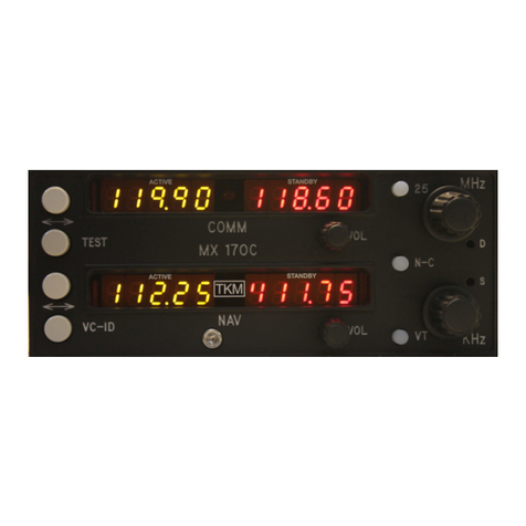
TKM MX385 User manual

1
INSTRUCTION MANUAL
FOR
MX385 NAV/COMM TRANSCEIVER
11/16/98 1/15/02 07/29/08
1 2 3 4 5
TKM, INC
14811 N. 73
RD
STREET
SCOTTSDALE, AZ 85260
PART # IMN385, REV. 5
JULY 29, 2008

2
TABLE OF CONTENTS
TITLE PAGE 1
TABLE OF CONTENTS 2
I. INTRODUCTION 3
A. Purpose of Equipment 3
B. Equipment Description 3
C. Specifications 5
II. INSTALLATION 7
*Notice to Installer* 7
*Continued Airworthiness (HBA 98-18)* 7
III. HOW TO OPERATE 8
IV. THEORY OF OPERATION 11
V. ALIGNMENT AND TEST SPECIFICATIONS 14
VI. MECHANICAL DISASSEMBLY 16
VII. TEST PROCEDURES 17
VII. SCHEMATICS, LAYOUTS AND PART LISTS 27
MX385 Interconnect (J1) 27
MX385 Interconnect (J2) 28
IDENTURED LIST OF DRAWINGS 29
Top Assembly 31
Computer 41
Front Panel 51
Display 57
Driver 62
Rear Panel 66
Rear Panel Assembly 76
Connector Board 86
T/R Switch 89
COMM Receiver 94
COMM Synthesizer 109
Transmitter 117
NAV Receiver 130
NAV Synthesizer 143

3
I. INTRODUCTION
This manual contains information on the Michel MX385, manufactured by TKM, Inc.
The information includes operational, mechanical, electrical descriptions, alignment and
test considerations.
A. Purpose of Equipment
The equipment is a 760 channel communication (COMM) transceiver for use in aviation
services and a 200 channel navigation (NAV) receiver to provide VOR/LOC signals to
navigational converters. The NAV receiver also provides frequency selection for remote
mounted Distance Measuring Equipment and Glideslope Receivers.
The MX385 is designed to be used as a direct replacement for the Cessna/ARC RT385A.
The unit is dimensionally identical to the ARC units and can therefore use existing
aircraft installations. Except for improved performance characteristics, the unit is
electrically interchangeable with the ARC unit and will provide the proper audio,
navigation signal and channeling signals for existing installations. New installations can
be made using RT385A installation kits.
B. Equipment Description
The unit features digital (LED) displays for active (yellow) frequency channel and
standby (red) frequency channel for both COMM and NAV.
For channel selection a MHz knob and a KHz knob are provided. For 25 KHz
increments in COMM, a 25 KHz button is provided. To activate COMM or NAV
frequency selection, an N/C button is provided; a ‘tic’ appears in the selected standby
channel display.
Channel selection operates on the standby channel only. When the desired channel is
indicated in the standby display it may be placed into the active position by depressing
the ‘Flip-Flop’ button located to the left of the displays; the active channel is then placed
into the standby position.
The NAV receiver features a VC/ID button to permit selection of voice or Ident
reception. In the Ident condition a ‘tic’ is displayed on the active NAV channel display.
The COMM transceiver features a test button, which overrides the squelch to verify
proper receiver operation and to allow reception of weak signals. Also provided on the
active COMM display, is a ‘tic’ to indicate transmitter power output.
The master power switch is integrated with the COMM volume control.

4
A VOR test button (VT) is provided for testing navigational systems; depressing the
button provides a ground on the appropriate rear panel contact.
The adjustment hole (D) by the MHz switch permits operator adjustment of the display
dimmer range for optimum nighttime viewing. The adjustment hole (S) by the KHz
switch permits operator adjustment of the squelch threshold.
The MX385 is comprised of eight replaceable subassemblies; five of the subassemblies
are contained in shielded modules to reduce radio frequency interference. The five
modules are the NAV receiver, the NAV synthesizer, the COMM receiver, the COMM
synthesizer, and the Transmitter.
The remaining three subassemblies are the Rear Panel Assembly, the Front Panel
Assembly and the Computer Board. The Rear Panel Assembly contains the Audio
Amplifier, the power converter, the Power Line Filter, and the T/R switching. The Front
Panel Assembly contains the digital displays and associated driver circuits, the functional
select switches and the volume controls. The Computer Board contains the
microprocessor, the memory, the Program storage, and the Channeling circuitry.
Also contained on the computer board are the audio processing circuits.
The subassemblies are interconnected with plugs to facilitate module replacement. For
equipment repair it is recommended that complete subassemblies be replaced.
As an aid to locating the defective subassembly a set of analog test points are provided.
The analog test points include the receiver tuning voltages, the synthesizer control
voltages and the AGC lines.

5
C. SPECIFICATIONS
MX385 TRANSCEIVER
Mounting: Panel mounted, no shock mounting
required.
Size: 6.312 x 2.50 x 11.1 inches w/
connectors but excluding knobs.
Weight: 6.0 lbs excluding external connector
and harness.
Power Requirements: 27.5 Vdc at 0.7 Amp
Max COMM Total w/
Transmit (Tone) 3.0 Amp
COMM TRANSCEIVER
Crystal Controlled: 760 Channel
Frequency Range: 118.00 to 135.975 MHz
Frequency Stability: +/- .003%. –20 to 50 C
TRANSMITTER
VHF Power Output: 8 watts minimum, 50 ohm
Modulation: 85% capability with 90% limiting
provided.
Microphone: Dynamic mike containing
transistorized pre-amp or carbon
(must provide at least 120 mV rms
into 500 ohm load)
Sidetone: Adjustable up to 40 mw into 500 ohm
headphones.
Duty Cycle: 1 minute on, 4 minutes off (20%)

6
RECEIVER
Sensitivity: 1.5 uv (soft) will provide a 6 db
minimum signal plus noise ratio
(KHz, 30% mod).
Selectivity: Typical 6 db at +/- 7.5 KHz, 65 db at
+/- 17.5 KHz, 90 db at +/- 25 KHz.
Spurious Responses: Down at least 70 db
Ident Filter: 15 db minimum
AGC Characteristics: From 2 to 100.000 uV audio output
will not vary more than 1 db.
NAV Receiver Accuracy: Two sigma limit, +/- 1 degree
NAV Output: With LOC adjusted for 0.35 Vrms
VOR = 0.5 Vrms (typical) into 20K
ohms or greater load impedance.
DME Channeling: 2 x 5
G/S Channeling: 2 x 5
AUDIO
Auxiliary Audio Inputs: Eight 500 ohms with 30 db isolation
between any two.
Frequency Response: Within 6 db from 350 Hz to 2500
Hz
Headphone Output: 40 mw into 500 ohm
Speaker Output: 4.5 Vrms into auxiliary input
produces 5 watts audio output.

7
II. INSTALLATION
The MX385 is designed to be an exact replacement for the ARC RT385A and similar
units. As a replacement unit, the MX385 is inserted directly into the mounting tray for
the RT385A and tightened down with a long (11” shaft by .150” diameter) standard
screwdriver.
For new installations, ‘Installation Instructions’ for the RT385A should be used.
To remove the MX385 from the mounting tray it is important to note that the Channel
Selector knobs should not be used. The first step in removal is to ensure that the
mounting screw has been fully disengaged by rotating the mounting screw
counterclockwise with the tool described above. The unit should then easily slide
forward by grasping the sides of the front panel.
NOTICE TO INSTALLER
The TKM MX385 NAV/COMM is authorized by the FAA to TSO C34e, C36e, C37d, C38d, and C40c. The product is
an incomplete system. In order to achieve a complete TSO quality system, the MX385 must be installed to configure
in conjunction a TSO C37/C38 authorized antenna and a TSO C34 authorized navigation receiver. It is the
responsibility of the installer to ensure proper installation.
CONTINUED AIRWORTHINESS (HBA 98-18)
Permission is hereby given to installers approved by the recognized aviation authority to reference relevant excerpts
from the installation instructions provided by TKM, Inc. in order to fulfill documentation requirements for Instructions
for Continued airworthiness. Adequacy of the documents should not be assumed by this permission. Responsibility
for ICA documentation rests solely with the applicant. The MX385 product is ‘Repair on Condition Only’.

8
III. HOW TO OPERATE
Operating controls for the MX385 are located on the unit front panel or are remote inputs
through the rear panel.
The unit front panel is shown in fig. 1. The upper left-hand (yellow) COMM readout
indicates the active COMM frequency and the right-hand (red) COMM readout indicates
standby COMM frequency. The lower left-hand (yellow) readout indicates the active
NAV frequency and the right-hand (red) NAV readout indicates the standby NAV
frequency. A ‘tic’ readout is provided on the upper left-hand corner of the first digit of
each of the four frequency readouts.
The active COMM ‘tic’ indicates the presence of transmitter power.
The standby COMM ‘tic’ indicates that the Frequency Selection knobs will control
COMM standby frequency.
The active NAV ‘tic’ indicates that the NAV receiver is in the Ident mode.
The standby NAV ‘tic’ indicates that the Frequency Selector knobs will control NAV
standby frequency.
Power Application. The COMM volume control contains the master power switch and
activates both the NAV and COMM functions.
Frequency Selection. Then N/C button is used to activate either the COMM or the NAV
frequency selection as indicated by the appropriate “‘‘tic’’” display. The MHz and KHz
controls can then be used to select a desired standby channel. In COMM the ‘25’ button
is used to advance the frequency by 25 KHz.
After the desired standby frequency is selected it may be transferred to the active position
by pressing the Flip-flop button to the left of the ACTIVE display. The active and
standby channels will be interchanged each time the button is pressed.
Ident/Voice Selection. The ID\VC button can be used to select a tone filter in order to
receive voice signals on the NAV receiver. The switch is also used for frequency storage
as described below.
Test. The TEST button is a dual function switch. In normal operation, it is used to
override the squelch to verify receiver operation and to receive weak signals. The switch
is also used for frequency storage as described below.

9
Frequency Storage. The MX385 NAV COMM allows up to 50 NAV and 50 COMM
preset frequencies to be stored in the memory for recall. The use of memory presets is
described in the following sections.
Clearing all frequency presets. To erase all frequency presets with one operation,
simply turn on the power to the radio while holding the TEST button depressed.
Examining/Changing/Inserting/Deleting frequency presets. These operations on
individual frequency presets are accomplished in EDIT mode. To enter EDIT mode, turn
on the power to the radio while holding the VT button depressed. When the radio is in
EDIT mode, the ACTIVE displays show the reference number of the preset and the
standby displays show the actual preset frequency. After the ‘clearing all frequency
presets’ operation as described above, the only presets of 121.5 and the default NAV
preset of 112.0 are displayed.
EDIT mode operations are performed on either the COMM or NAV preset list, according
to where the tuning ‘tic’ indicator is displayed. The tuning ‘tic’ appears immediately to
the left of the COMM or NAV standby displays. Pressing the N/C button toggles
between NAV and COMM preset editing.
Examining presets (EDIT MODE). Pressing the COMM F-F button will step to the next
frequency in the preset list. Pressing the TEST button will step to the previous frequency
in the preset list. Pressing COMM F-F when the last preset is displayed will cause the
first preset to display. Similarly, pressing TEST when the first preset is displayed will
cause the last preset to display. Warning: When there is only one preset in the list, the
radio will not appear to “do anything” when the COMM F-F or TEST is pressed. This is
because the current, previous, and next presets are all the same preset.
Changing a preset (EDIT MODE). Press COMM F-F or TEST until the preset to be
changed is displayed. Dial in the new preset frequency using the tuning controls and
press either COMM F-F or TEST.
Inserting (Adding) a preset (EDIT MODE). Press COMM F-F or TEST until the desired
insert point is displayed (the new preset will be inserted AFTER this insert point). Dial
in the desired frequency using the tuning controls and press NAV F-F. Remember that a
preset list may contain a maximum of 50 entries. Inserting presets that would exceed this
limit are ignored.
Deleting a preset (EDIT MODE). Press COMM F-F or TEST until the preset to be
deleted is displayed. Then press the VC-ID switch to delete. If the deleted preset was
not at the end of the list, all the presets that followed it are renumbered. Each preset list
(NAV and COMM) must always contain at least one entry. If there is only one entry
remaining in a preset list, it may not be deleted (It can, however, be changed to another
frequency).

10

11
IV. Theory of Operation
For ease of service the MX385 has been designed into 8 replaceable modules. The
modules are: A. Front Panel Assembly
B. Rear Panel Assembly
C. Computer Board
D. NAV Receiver
E. COMM Receiver
F. NAV Synthesizer
G. COMM Synthesizer
H. Transmitter
A block diagram is shown in drawing AT1900, Top Assembly
A. Front Panel Assembly (Dwg. SS1930)
The front panel includes the four frequency displays, a photocell for automatic brightness
control, 7 push buttons, two volume controls (the COMM control incorporates the power
switch) and two frequency selection switches. The displays and controls are connected to
the display driver board through pin and socket connectors and to the computer board
with a ribbon cable
.
B. Rear Panel Assembly (Dwgs. SS1945, SS1940)
The rear panel includes the power converter, the audio circuits and T/R switching
circuits.
The audio is amplified in IIA and then selected with Q13. The audio is inverted in IIB
and further amplified in Q3 and Q4. IIC is used to monitor the DC current flowing in Q3
and Q4 and adjust the bias so that the current is 0.20 Adc.
The modulation amplifier consists of I4, Q11 and Q12. Diodes D19 and D20 provide
peak to peak limiting of the microphone input signal to prevent modulation splatter. C2,
C25 and C28 provide high frequency roll-off to prevent adjacent channel interference.
Q2, Q8, Q9, Q10 and Q13 are all used in the T/R switching.
Q15 drives the PIN diode in the T/R switch so that in the transmit mode the drive
impedance is very high and in the receive mode 5 mA of turn-on current is provided.
Q14 is an FET Power Switch controlled by the front panel power switch. When Q1 is
switched on Q1 is also switched on to provide external NAV power.
I3 is a switching regulator that drives Q7 and converts the input line voltage (20 –32 vdc)
to a regulated 5.2 vdc. Q5 and Q6 form a free-running inverter and supply approximately
+20 vdc. The +20 vdc supply is regulated by I2 to provide a stable +15 vdc supply.
The T/R Switch (Dwg. SS1921) contains switching diode D1 and a low pass filter L1,
C2, L2, C3. In receive mode, the diode is forward biased to couple the receiver to the

12
antenna. In transmit, the T/R line is open circuited to permit the transmitter signal to
generate a reverse bias on the diode to the peak value of the transmit signal.
C. Computer Board (Dwg. SS1967)
The computer board contains 3 basic sections:
1. Computer
2. Analog Processing
3. Channeling Circuits
1. Computer
The computer is comprised of the processor (I6), the Program Prom (I5), the Memory
Ram (I4), the address decoder (I7, the oscillator (I3), and the read-write decoder (I8).
The Ram contains a lithium battery that will support the memory indefinitely.
2. Analog Processing
The Analog Processing functions include noise detection, phone amplification, tracking,
squelch, Ident code filtering and transmitter monitoring.
I12B is an adjustable gain amplifier used to track receiver tuning to synthesizer
frequency. I12A and I12D is a 2-pole bandpass filter to separate noise from audio
signals. The noise is detected with D4. The noise level is used to inhibit the carrier
squelch threshold as determined by I13B.
I13A detects the voltage on the T/R switch. When a large negative voltage is detected, an
active signal is applied to I1 to turn on the transmit ‘tic’.
I11 is the NAV phone amplifier. I18 provides volume compression for the COMM audio
and I19 is the COMM phone amplifier.
3. Channeling Circuits
The channeling circuits are comprised of digital latches and output drivers. I16 provides
MHz output signals, the ILS Energize Signal and the VOR Test signal. I15 provides
KHz output signals. NPN transistors are used as output drivers. For Glideslope
channeling the drivers are connected directly to the output pins, for DME channeling
isolation diodes are provided in each line.
D and E. NAV (Dwg. SS1867) and COMM (SS1866) Receivers
The NAV and COMM receivers are functionally the same. The only difference between
the two receivers is the RF tuning, the AGC time constant and a tuning voltage sensor in
the COMM receiver which reduces the receiver gain during Transmitter actuation.
COMM Receiver tuning:
1. Connect a Synthesizer and Receiver combination to a NAV/COMM assembly.

13
2. Using a Spectrum Analyzer with a tracking generator align RF filters to have a
symmetrical response centered at 136.9 MHz when NAV/COMM unit is tuned to
136.9 MHz. Peak gain shall be 15 +/- 1.5 DB when output is measured at mixer input.
3. Apply –99 dbm at 136.9 MHz with 30% modulation. Peak the IF coil and adjust the
AGC pot for 6.0 volts on the AGC line. Adjust the Audio gain pot for 4.0 vp-p on
Audio Output.
NAV Receiver tuning:
1. Use the COMM Receiver procedure except use 117.9 MHz for the test channel.
F and G. NAV (Dwg. SS2714) and COMM (SS2716) Synthesizers
The NAV and COMM synthesizers are identical except for tuning and an additional
output is provided in the COMM synthesizer to drive the transmitter.
COMM Synthesizer tuning
1. Connect COMM Synthesizer to an operating NAV/COMM assembly and monitor
receiver and transmitter outputs with RF Voltmeter. Monitor Tuning voltage with a
DC Voltmeter and Transmitter output with a Sideband Monitoring system capable of
measuring 25 KHz sideband signals.
2. Set NAV/COMM assembly to 136.95 MHz in Receive mode. Adjust tuning voltage
with R8 to 10.0 vdc.
3. Verify a tuning voltage of about 6 vdc at 118.7 MHz.
4. Receiver RF output shall be 9.0 +/- 1 db.
5. Select transmit mode and Transmit RF shall be 9.0 +/- 2 db.
6. Adjust R7 to null 25 KHz sidebands on the Transmitter output.
NAV Synthesizer tuning
1. Connect NAV Synthesizer to NAV/COMM Assembly and monitor tuning voltage and
RF output.
2. Select channel frequency of 117.95 MHz and adjust turn spacing on synthesizer for
7.0 vdc on tuning line.
3. RF output shall be 9.0 +/- 1 db.
H. Transmitter (Dwg. SS1881)
The transmitter consists of 4 RF power amplifiers. The first amplifier Q4 is gated on by
power received from the frequency synthesizer. Q1, Q2, and Q3 form a broad-band
collector modulated transmitter chain.

14
V. Alignment and Test Specifications
Adjustments are made on the complete unit during final test basis and upon installation
basis. Installation adjustments are accessible without removing the cover and include a
side tone level adjustment, a microphone gain adjustment, and an audio gain adjustment.
Other adjustments which are not normally adjusted on installation but may require
adjustment different from factory set levels include the squelch level, the dimmer and the
NAV demod level.
A spectrum analyzer is required only for frequency alignment of the Synthesizer module.
If Synthesizer repair is made on a replacement basis, it is not necessary to have a
spectrum analyzer for field service.
Module Alignment
A. Front Panel Assembly (Dwg. SS1930)
The front panel requires no alignment
B. Rear Panel Assembly (Dwgs. SS1945, SS1940)
The rear panel contains three potentiometers which are adjusted as follows:
1. Audio Gain: Apply 3 v rms at 1000 Hz to an aux. audio input and adjust R5 (Audio
Gain) for 5 Watts into a 4 ohm load on the speaker output.
1. Microphone Gain: (R46): Apply .30 Vrms at 1000 Hz to pin 13 of P1. Adjust R46
so
that 12 v p-p is output to the transmitter modulation line.
2. Sidetone Level (R1). Apply .30 vrms at 1000 Hz to pin 13 of P1 and adjust R1 so
that 1.0 vrms appears across a 500 ohm load connected to pin 18 of P1.
C. Computer Board (Dwg. SS1967)
The computer board contains mostly system alignment adjustments which can be set only
with a complete unit. The clock frequency, however, can be set on the board level.
1. Clock Frequency (C5):Adjust C5 so that frequency measured on pin 8 of I2 is
1,000,000 +/- 10 Hz at 70 degrees F room temperature.
D. NAV Receiver (Dwg. SS1867)
1. Apply +15 vdc and –30 vdc to appropriate input leads, local oscillator signal at 3.0 + 2
dbm and a 0 to 14 vdc variable voltage source to Vt.
2. IF Alignment (L2, L3, L4). Apply +7.0 vdc to Vt, 117.90 MHz at –90 dbm to RF in
and 96.50 MHz at +3 dbm to L.O. Adjust L2, L3 and L4 for minimum voltage reading
on Vagc. Apply amplitude modulation of 30% and monitor DMD output. As the
modulation frequency is adjusted from 1.0 to 12.0 Khz the DMD level shall be constant
+/- 1 db. Adjust L2 and L3 as necessary to keep DMD level constant.
3. RF Alignment (T1, T2, L1, T3). With conditions the same as in IF Alignment, but
modulation set to 0, adjust turn spacing on T1, T2, L1, and T3 so that Vagc reading is a
minimum.
4. Change RF to 108.00 MHz and L.O. to 86.60 MHz. Adjust Vt for minimum Vagc.

15
5. DMD Level (R25). With conditions the same as in IF Alignment apply a standard
centered LOC modulation and adjust R25 for .35 Vrms on DMD output.
E. COMM Receiver (Dwg. SS1866)
1. Apply +15 vdc and –30 vdc to appropriate input leads, set local oscillator signal to 3
+/-2 dbm and a 1 to 15 vdc variable voltage source to Vt.
2. IF Alignment (L2, L3, L4). Apply +10 vdc to Vt, 135.975 MHz at –90 dbm to RF and
157.175 MHz to L.O. Adjust L2, L3 and L4 for minimum voltage reading on Vagc.
Apply amplitude modulation of 30% and frequency is adjusted from 1.0 to 12.0 KHz the
DMD level shall be constant +/- 1 db. Adjust L2 and L3 as necessary to keep DMD level
constant.
3. RF Alignment (T1, T2, L1, T3). With conditions the same as in IF Alignment but
modulation set to 0, adjust turn spacing on T1, T2, L1 and T3 so that Vagc reading is a
minimum.
F. NAV Synthesizer (Dwg. SS2714)
1. Apply +15 vdc and 1 MHz to appropriate module input. Set R3 to midrange.
Digitally input, using Computer board or equivalent, the proper coding for 96.50 MHz.
Verify correct output frequency. Adjust turn spacing on T1 so that Vt = 7.00 vdc.
Digitally input coding for 86.60 MHz. Vt shall be 2.50 +/- .30 vdc.
2. Digitally input coding for 91.60 MHz and monitor output on a spectrum analyzer.
Adjust R3 so that 50 KHz sidebands are nulled.
G. COMM Synthesizer (Dwg. SS2716)
1. Apply +15 vdc and 1 MHz to appropriate module input. Set R3 to midrange.
Digitally input, using Computer board or equivalent, the proper coding for 157.30 MHz.
Verify correct output frequency. Adjust turn spacing on T1 so that Vt = 10.00 vdc.
Digitally input coding for 139.40 MHz. Vt shall be 5.00 +/- .50 vdc.
2. Digitally input coding for 149.00 MHz and monitor output on a spectrum analyzer.
Adjust R3 so that 25 KHz sidebands are nulled.
H. Transmitter (Dwg. SS1881)
The Transmitter does not normally require alignment but tests should be performed to
verify proper operation.
1. Connect the transmitter to a properly aligned COMM Synthesizer and connect a 50
ohm load to the Transmitter output. Monitor the output power level to verify that it is at
least 9.0 watts without modulation across the frequency range of 118 to 136 MHz. Apply
at least 80% modulation at 1.0 KHz and monitor the output with a spectrum analyzer to
verify that no parasitic oscillation is present. If problems are encountered, consult the
factory.

16
System Alignment
When all modules are aligned and assembled into a system, it is necessary to make
receiver tracking, VOR/LOC converter and squelch adjustments.
COMM receiver tracking is accomplished by selecting 118.00 MHz as the active channel,
applying a 10 uV RF input signal at 118.00 MHz, and adjusting R49 on the Computer
board for minimum reading on COMM AGC line.
NAV receiver tracking is accomplished by selecting 108.00 MHz and adjusting R33 on
the Computer board for a minimum reading on NAV AGC.
Carrier squelch is adjusted by applying an unmodulated carrier at 2.0 uV to the COMM
receiver and adjusting R29 on Computer board, to just break squelch.
Noise inhibit is adjusted by applying a carrier with 30% modulation at 6.666 KHz to the
COMM receiver and adjusting R31 on the Computer board so that a 10 uV signal will
just break squelch.
Demod output level is set by R71 (Demod Level).
The 1020 Hz Filter is adjusted by monitoring the audio output and applying a 1020 Hz
modulation to the NAV Receiver input. With ‘Voice’ selected, adjust R12 (1020 Hz) for
minimum tone output.
VI. Mechanical Disassembly
The first step in mechanical disassembly is to remove the top cover by removing the nine
screws around the sides and rear of the cover. The cover may then be pried up at either
rear corner lifted slightly and slid away from the front panel.
The computer board is removed by first disengaging the connectors and then removing
the six spacers holding the computer board. The board may then be lifted from the unit.
The front panel may be disengaged by removing four screws from the sides and bottom,
and disconnecting the connectors.
The rear panel is removed by removing two screws on the bottom of the unit and one
screw from each side of the unit, and disconnecting the connectors. The transmitter
power lead can be removed by loosening the attaching screw.
The RF modules may be removed by removing the mounting screws from the bottom of
the unit and disconnecting the connectors.

17
SECTION VII
TEST PROCEDURES

18

19

20
Table of contents
Other TKM Transceiver manuals
