TL Electronic EL1083 User manual

86(5
86(586(5
86(5·
··
·6
66
6
0$18$/
0$18$/0$18$/
0$18$/
6OLPDQG)DQOHVV,QWHO
((-
SURFHVVRU(PEHGGHG3&
$+
TL Electronic GmbH
Bgm.-Gradl-Str. 1
85232 Bergkirchen-Feldgeding
Germany
Tel.: +49 (0)8131 33204-0
Fax: +49 (0)8131 33204-150
www.tl-electronic.de
5DQRHNMÐ

Contents
GDD!OPUJDF
This equipment has been tested and found to comply with the limits for a Class A
digital device, pursuant to part 15 of the FCC Rules. These limits are designed to
provide reasonable protection against harmful interference when the equipment is
operated in a commercial environment. This equipment generates, uses, and can
radiate radio frequency energy and, if not installed and used in accordance with the
instruction manual, may cause harmful interference to radio communications.
Operation of this equipment in a residential area is likely to cause harmful interference
in which case the user will be required to correct the interference at his own expense.
You are cautioned that any change or modifications to the equipment not expressly
approve by the party responsible for compliance could void your authority to operate
such equipment.
!
WARNING! Some internal parts of the system may have high
electrical voltage. And therefore we strongly recommend that
qualified engineers can open and disassemble the system.
RESTRICTED ACCESS LOCATION: access can only be gained by
SERVICE PERSONS or by USERS who have been instructed about
the reasons for the restrictions applied to the location and about any
precautions that shall be taken; and access is through the use of a
TOOL or lock and key, or other means of security, and is controlled
by the authority responsible for the location

Contents
TABLE OF CONTENTS
CHAPTER 1 INTRODUCTION
1-1 About This Manual.................................................................... 1-2
1-2 System Illustration...................................................................... 1-3
1-3 System Specifications................................................................. 1-5
1-4 Safety Precautions...................................................................... 1-7
CHAPTER 2 SYSTEM CONFIGURATION
2-1 Jumper & Connector Quick Reference Table............................. 2-2
2-2 Component Locations................................................................ 2-3
2-3 How to Set the Jumpers.............................................................. 2-5
2-4 PWR In Connector……..………………………….................... 2-7
2-5 COM Port & Connector……..…………………………............ 2-7
2-6 COM Port RI & Voltage Selection............................................ 2-10
2-7 USB Port…………………..…………………………………... 2-10
2-8 LAN Port………........................................................................ 2-12
2-9 DVI Connector........................................................................... 2-14
2-10 Digital I/O Connector…...………………………………….. 2-16
2-11 Audio Connector…………..…………………………………... 2-17
2-12 SATA & SATA Power Connector............................................. 2-18
2-13 CFAST Card Slot...……………………………………………. 2-19
2-14 CFAST Card Power Selection
įįį
.………………………............ 2-19
2-15 Clear CMOS Data Selection…...………………………............ 2-20
2-16 DVI-D Enable Selection…...……………………….................. 2-20
2-17 DVI-D HPD Enable Selection…...……………………............. 2-21
2-18 DDC Selection……………………………………………….... 2-21
CHAPTER 3 SOFTWARE UTILITIES
3-1 Introduction................................................................................ 3-2
3-2 Intel
®
Chipset Software Installation Utility…..…….................. 3-3
3-3 Intel ® Trusted Execution Engine Driver installation…………
3-4 Intel ® Kernel-Mode Driver Framework Driver Installation….
3-4
3-5
3-5 Intel® Mailbox Interface Device Driver………….…………... 3-6
3-6 For USB3.0 Driver installation………………………………... 3-7
3-7 VGA Driver Utility.................................................................... 3-8
3-8 LAN Driver Utility..................................................................... 3-9
3-9 Sound Driver Utility................................................................... 3-10

Contents
CHAPTER 4 SYSTEM INSTALLATION
4-1 Removing the bottom case......................................................... 4-2
4-2 HDD Installation........................................................................ 4-4
4-3 SO-DIMM Installation……....................................................... 4-8
4-4 Wireless LAN or 3G module Installation…………................... 4-12
4-5 CFast Card Installation……………........................................... 4-17
4-6 PoE Board Installation…………………………………….…... 4-21
CHAPTER 5 AMI BIOS SETUP
5-1 Introduction................................................................................ 5-2
5-2 Entering Setup............................................................................ 5-4
5-3 Main……................................................................................... 5-6
5-4 Advanced…………………….........................…....................... 5-8
5-5 Chipset…………….................................................................... 5-43
5-6 Security………………………………………………………... 5-53
5-7 Boot..……………….................................................................. 5-54
5-8 Save & Exit……………………………………………………. 5-58
APPENDIX A SYSTEM ASSEMBLY
Exploded Diagram for Bottom Case………..….................................... A-2
Exploded Diagram for HDD Support Board.….................................... A-3
Exploded Diagram for Front & Rear Case…….................................... A-5
Exploded Diagram for Motherboard……..……................................... A-6
Exploded Diagram for Heatsink……………….................................... A-7
APPENDIX B TECHNICAL SUMMARY
Block Diagram...................................................................................... B-2
Interrupt Map......................................................................................... B-3
I/O Map................................................................................................. B-8
Memory Map………………………………………………………….. B-11
Watchdog Timer Configuration…………..…………………………... B-13
Flash BIOS Update……………………………………………………. B-15
!
!
!

Page:1-1
!
!
!
!
!
!
!
INTRODUCTION!
!!
!
!
!
!
This chapter gives you the information for EL1083. It also outlines
the System specification.
Section includes:
zAbout This Manual
zSystem Specifications
zSafety Precautions
Experienced users can skip to chapter 2 on page 2-1
for Quick Start.
!
CHAPTER
1
!

Chapter 1 Introduction
!
!!
!
Page: 1-2
1-1. ABOUT THIS MANUAL
!
Thank you for purchasing our EL1083 Intel
®
E3845/E3826/J1900 Embedded PC.
EL1083 provides faster processing speed, greater expandability and can handle more
task than before. This manual is designed to assist you how to install and set up the
system. It contains four chapters. The user can apply this manual for configuration
according to the following chapters:
Chapter 1 Introduction
This chapter introduces you to the background of this manual, and the specifications
for this system. The final page of this chapter will indicate how to avoid damaging
this board.
Chapter 2 Hardware Configuration
This chapter outlines the component locations and their functions. In the end of this
chapter, you will learn how to set jumper and how to configure this card to meet your
own needs.
Chapter 3 Software Utilities
This chapter contains helpful information for proper installations of the VGA utility,
LAN utility, and Sound utility.
Chapter 4 AMI BIOS Setup
This chapter indicates you how to set up the BIOS configurations.
Appendix A System Assembly
This appendix gives you the exploded diagrams and part numbers of the (/.
Appendix B Technical Summary
This appendix gives you the information about the Block diagram, Technical maps,
Watchdog-timer configuration, and Flash BIOS Update.

Chapter 1 Introduction
!
!!
!
Page: 1-3
1-2. SYSTEM ILLUSTRATION
Front View
46
DVI-D
COM4COM3 Remote SW
DIO
ANT2
Rear View
GND VCC
Reset
COM2
COM1
DVI-I
PoE ANT1
ON
LAN1 LAN2
Top View Quarter View
217.50
Chapter 1 Introduction
!
!!
!
Page: 1-4
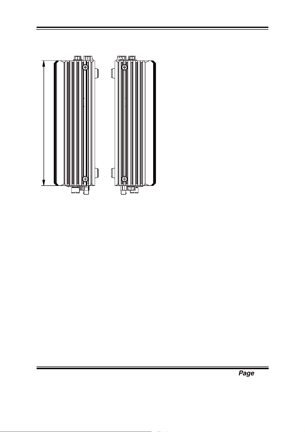
Side View
140.60

Chapter 1 Introduction
!
!!
!
Page: 1-5
1-3. SYSTEM SPECIFICATION
System
CPU Support Intel® J1900/E3845/E3826 CPU
Chipset Intel® SOC
OS Support Win7/ Win8.1/ WES7/ WE 8.1 Industry Pro
Memory Support 1 x DDR3L SO-DIMM Socket (up to 8 GB)
Drive Bay 1 x 2.5 inch SATA HDD or SSD driver space
Power Requirement 9~36V DC-in
Watchdog 1~255s Watchdog timer
Expansion Slot 1x full size miniPCIe (PCIe+USB+external SIM card)
1x half size miniPCIe (PCIe+USB)
System Weight 2.5 kg
Dimension (W x H x D) 217.5 x 46 x 148 mm (8.56” x 1.77” x 5.83”)
Certificate FCC/CE
I/O Ports
Serial Port COM3/4 for RS232 (front), COM1/2 for +5v/+12v/RI
selectable by jumper,RS232/422/485 selectable by BIOS
Digital I/O 4-in/4-out (front)
USB 1 x USB 2.0 port (front), 2 x USB 2.0, 1 x USB 3.0 (rear)
DVI DVI 1 x DVI-D (front), 1 x DVI-I (rear)
SIM 1 x SIM card slot with cover
SD 1 x SD Card with cover
Audio Realtek high definition audio, 1x Line-Out & 1x MIC In
audio jack by pin header
LAN 2 x RJ45 connector with PoE support Wake on LAN/
PXE
Power ON/OFF 1x power button switch (rear), 1x 2pin connector for
remote power button (front)
Reset 1x reset (rear)

Chapter 1 Introduction
!
!!
!
Page: 1-6
!
Environment
Operating Temp.
(withair)
0~45°C (32~113°F),with ST SSD
0~40°C (32~104°F), with HDD
-30~60°C (-22~140°F) with wide temp. peripherals w/o
PoE (w/o Audio) (E3845/E3826 only)
-30~55 °C (-22~131°F) with wide temp. peripherals with
PoE (w/o Audio) (E3845/E3826 only)
Storage Temp. -30 ~ 80°C (-22~ 176°F)
Humidity Operating: 10 ~ 90%, Storage: 10~95%RH

Chapter 1 Introduction
!
!!
!
Page: 1-7
1-4. SAFETY PRECAUTIONS
Follow the messages below to avoid your systems from damage:
1. Keep your system away from static electricity on all occasions.
2. Prevent electric shock. Don’t touch any components of this card when the card is
power-on. Always disconnect power when the system is not in use.
3. Disconnect power when you change any hardware devices. For instance, when
you connect a jumper or install any cards, a surge of power may damage the
electronic components or the whole system.
!

Page 2-1
HARDWARE
CONFIGURATION
** QUICK START **
CHAPTER
2
Helpful information describes the jumper & connector settings, and
component locations.
Section includes:
zJumper & Connector Quick Reference Table
zComponent Locations
zConfiguration and Jumper settings
zConnector’s Pin Assignments

Chapter 2 Hardware Configuration
Page: 2-2
2-1. JUMPER & CONNECTOR QUICK REFERENCE TABLE
JUMPER / CONNECTOR NAME
Pwr In Connector CN_POWER1
Com Port & Connector COM1, COM2, COM3, COM4, COM5,
COM6
Com Port Ri & Voltage Selection JPCOM1, JPCOM2
USB Port USB4, USB2, USB3, USB5
LAN Port LAN1, LAN2
DVI Connector DVI1, DVI2
Digital I/O Connector DIO1, JDIO1
Audio Connector JAUDIO1
SATA & SATA Power Connector SATA1, HDD_POWER1
CFast Card Slot CFAST1
CFast Card Power Connector JP11
Clear CMOS Data Selection JP1
DVI-D Enable Selection JP34, JP35
DVI-D HPD Enable Selection JP37
DDV Selection JP13
Chapter 2 Hardware Configuration
Page: 2-3
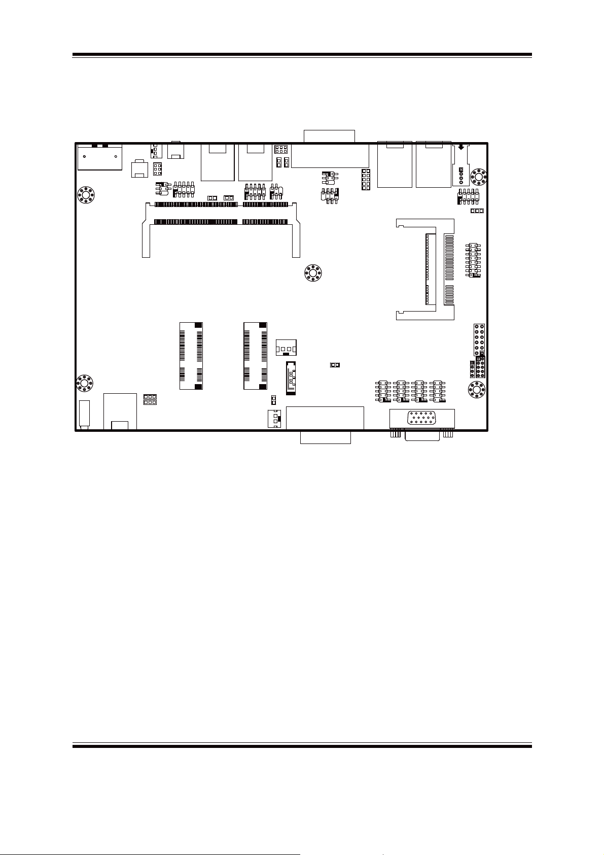
2-2. COMPONENT LOCATIONS
1
7
1
6
11 15
10
5
DIO1
DIMM1
CFAST1
SLOT1
USB3
DVI1
DVI2
USB4
SATA1
BAT1
JP11
USB5
10 9
21
S1 S7 PC1 PC17
12
12
1
15
17
51
2
16
18
52
1
203
204 2
1
3
COM3COM4COM5COM6
JP1
1
2
SATA_PWR1
JP37
SLOT2
1
15
17
51
2
16
18
52
JP35
JP34
3
3
1
1
LED1
CN_POWER1
12
SW2
JP36
1
2
JPCOM1
6
21
5
SW1
JP_COM1
COM1
JP17 JP18
21 21
LAN1 LAN2 USB2
11
JP19
JP20
JDIO1
JAUDIO1
12
JP10 JLPC1
JP9
JPOE1
JP13
JP3
JP_COM2
COM2
2
1
JPCOM2
Connectors, Jumpers and Components Locations - Front
Chapter 2 Hardware Configuration
Page: 2-4
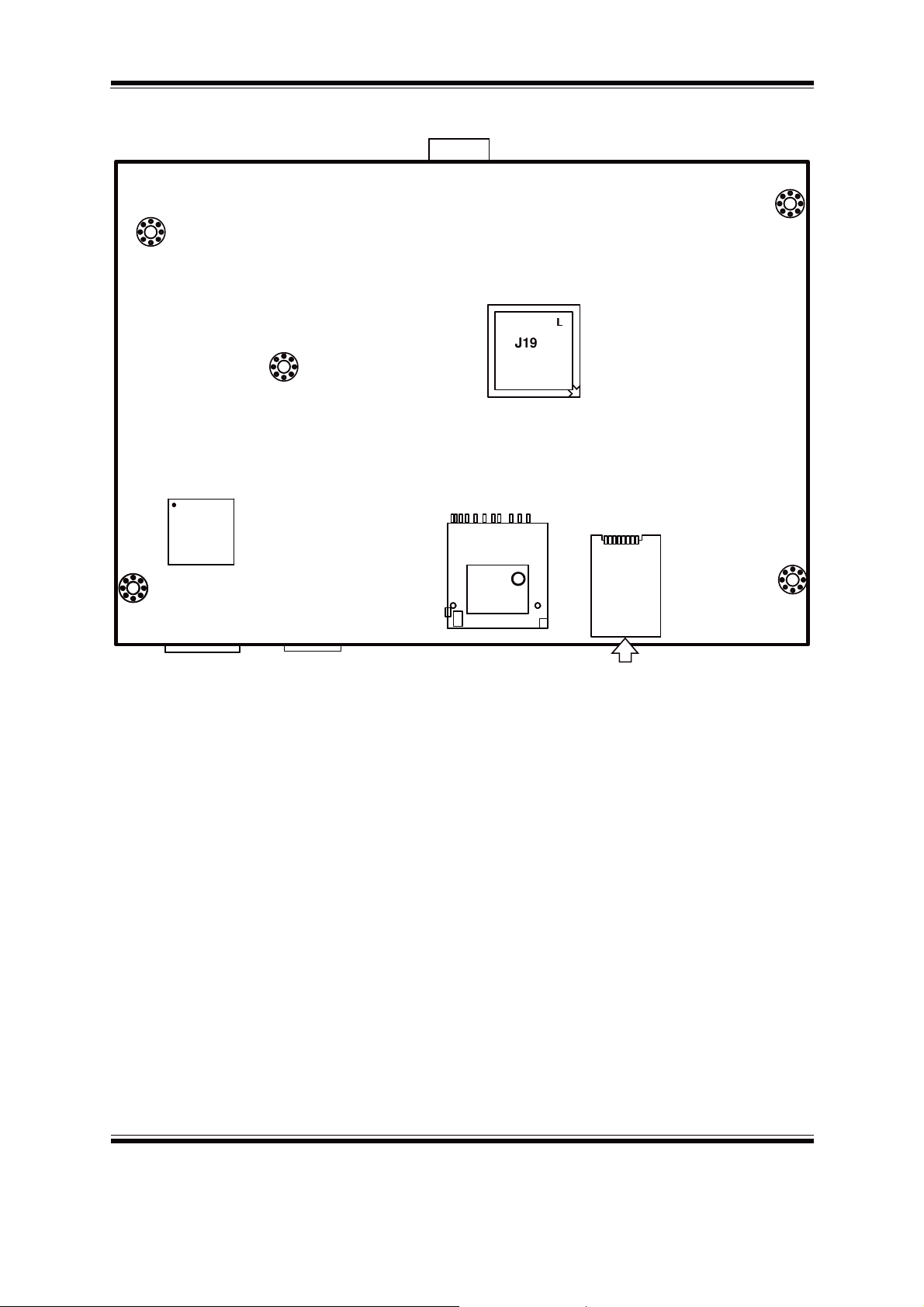
SIO
Intel®
ٞ
ٞٞ
ٞ
J1900/
E3845/
E3826
SIM1
SD_CARD1
Connectors, Jumpers and Components Locations - Rear

Chapter 2 Hardware Configuration
Page: 2-5
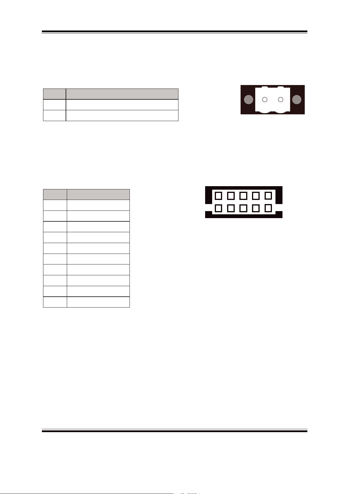
2-3. HOW TO SET THE JUMPERS
You can configure your board by setting jumpers. Jumper is consists of two or three
metal pins with a plastic base mounted on the card, and by using a small plastic "cap",
Also known as the jumper cap (with a metal contact inside), you are able to connect
the pins. So you can set-up your hardware configuration by "open"or "close"pins.
The jumper can be combined into sets that called jumper blocks. When the jumpers
are all in the block, you have to put them together to set up the hardware configuration.
The figure below shows how this looks like.
JUMPERS AND CAPS
If a jumper has three pins (for examples, labelled PIN1, PIN2, and PIN3), You can
connect PIN1 & PIN2 to create one setting by shorting. You can either connect PIN2
& PIN3 to create another setting. The same jumper diagrams are applied all through
this manual. The figure below shows what the manual diagrams look and what they
represent.

Chapter 2 Hardware Configuration
Page: 2-6
JUMPER DIAGRAMS
2 pin Jumper
looks like this
Jumper Cap
looks like this
3 pin Jumper
looks like this
Jumper Block
looks like this
JUMPER SETTINGS
Looks like this
3 pin Jumper
2-3 pin close(enabled)
Looks like this
Jumper Block
1-2 pin close(enabled)
2 pin Jumper close(enabled)
1
1
1212
1
1
Looks like this
Chapter 2 Hardware Configuration
Page: 2-7
2-4. PWR IN CONNECTOR
CN_POWER1: PWR IN Connector
The pin assignments are as follows:
PIN ASSIGNMENT
1 PWRI(9~36V)
ġ
2 GND
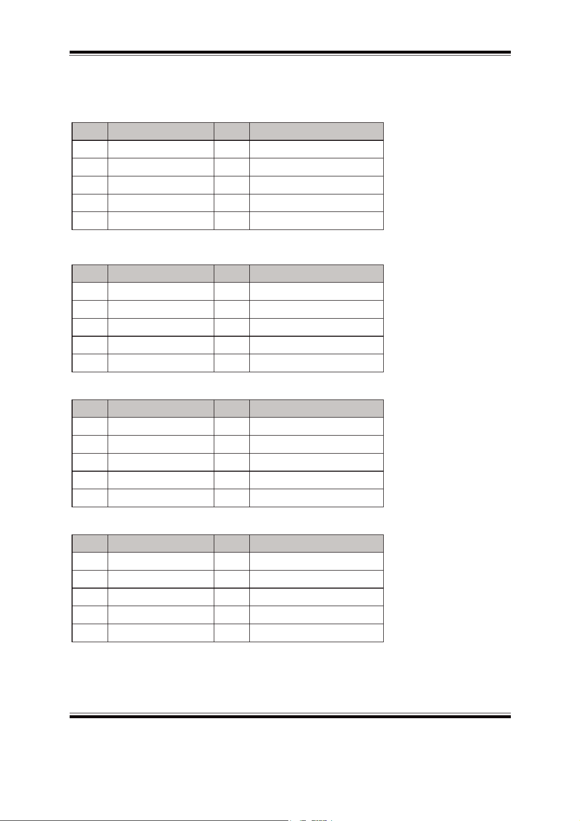
2-5.COM PORT & CONNECTOR
COM1: COM1 Connectors
The pin assignments are as follows:
PIN ASSIGNMENT
1 DCD1
2 RXD1
3 TXD1
4 DTR1
5 GND
6 DSR1
7 RTS1
8 CTS1
9
RI selectable
10
NC
12
&1B32:(5
51
10
6
&20&20&20
&20&20&20
Chapter 2 Hardware Configuration
Page: 2-8
COM1, COM2, COM3,COM4,COM5,COM6: COM Connectors
The pin assignments are as follows:
COM1:
PIN ASSIGNMENT PIN ASSIGNMENT
1 COM1_DCD_C 6 COM1_DSR_C
2 COM1_RX_C 7 COM1_RTS_C
3 COM1_TX_C 8 COM1_CTS_C
4 COM1_DTR_C 9 RI/+5V/+12 selectable
5 GND 10 NC
COM2:
PIN ASSIGNMENT PIN ASSIGNMENT
1 COM2_DCD_C 6 COM2_DSR_C
2 COM2_RX_C 7 COM2_RTS_C
3 COM2_TX_C 8 COM2_CTS_C
4 COM2_DTR_C 9 RI/+5V/+12 selectable
5 GND 10 NC
COM3:
PIN ASSIGNMENT PIN ASSIGNMENT
1 COM3_DCD_C 6 COM3_DSR_C
2 COM3_RX_C 7 COM3_RTS_C
3 COM3_TX_C 8 COM3_CTS_C
4 COM3_DTR_C 9 COM3_RI_C
5 GND 10 NC
COM4:
PIN ASSIGNMENT PIN ASSIGNMENT
1 COM4_DCD_C 6 COM4_DSR_C
2 COM4_RX_C 7 COM4_RTS_C
3 COM4_TX_C 8 COM4_CTS_C
4 COM4_DTR_C 9 COM4_RI_C
5 GND 10 NC
Chapter 2 Hardware Configuration
Page: 2-9
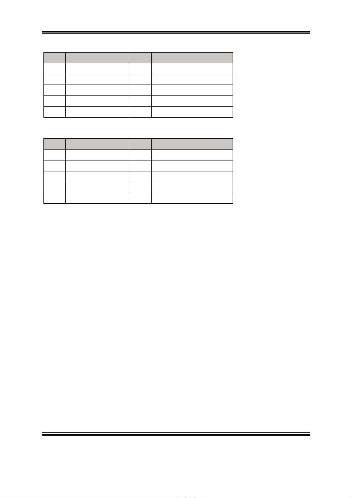
COM5:
PIN ASSIGNMENT PIN ASSIGNMENT
1 COM5_DCD_C 6 COM5_DSR_C
2 COM5_RX_C 7 COM5_RTS_C
3 COM5_TX_C 8 COM5_CTS_C
4 COM5_DTR_C 9 COM5_RI_C
5 GND 10 NC
COM6:
PIN ASSIGNMENT PIN ASSIGNMENT
1 COM6_DCD_C 6 COM6_DSR_C
2 COM6_RX_C 7 COM6_RTS_C
3 COM6_TX_C 8 COM6_CTS_C
4 COM6_DTR_C 9 COM6_RI_C
5 GND 10 NC
Note: COM1/2 connectors are selectable for RI, +5V or
+12V.For more information, please refer to COM
PORT & VOLTAGE SELECTION.
Table of contents
Other TL Electronic Desktop manuals


