Topway LMT035DNJFWD-NNA-1 User manual
URL: www.topwaydisplay.com
Document Name: LMT035DNJFWD-NNA-1-Manual-Rev0.2.doc
Page: 1 of 24
LMT035DNJFWD-NNA-1
LCD Module User Manual
Prepared by:
Ma Qi Yang
Checked by:
Approved by:
Date: 2022-02-23
Date:
Date:
Rev.
Descriptions
Release Date
0.1
Preliminary New release
2020-08-18
0.2
Update DC Characteristics
2022-02-23

TOPWAY
LCD Module User Manual
LMT035DNJFWD-NNA-1
URL: www.topwaydisplay.com
Document Name: LMT035DNJFWD-NNA-1-Manual-Rev0.2.doc
Page: 2 of 24
Table of Content
1. Basic Specifications...................................................................................................................3
1.1 Block Diagram................................................................................................................................................................3
1.2 Terminal Functions.........................................................................................................................................................4
2. Absolute Maximum Ratings......................................................................................................5
3. Electrical Characteristics..........................................................................................................5
3.1 DC Characteristics .........................................................................................................................................................5
3.2 LED Backlight Circuit Characteristics.............................................................................................................................6
4. AC Characteristics.....................................................................................................................6
4.1 DBI Type B.....................................................................................................................................................................6
4.2 3-Line SPI Interface Timing Characteristic...................................................................................................................11
4.3 4-Line SPI Interface Timing Characteristic...................................................................................................................12
4.4 DPI Interface ................................................................................................................................................................13
4.5 Power ON/OFF Sequence............................................................................................................................................16
4.6 Reset timing .................................................................................................................................................................17
5 . Optical Characteristics............................................................................................................18
6. LCD Module Design and Handling Precautions ..............................................................................................................21
7. CTP Mounting Instructions..............................................................................................................................................22
8. RTP Mounting Instructions..............................................................................................................................................23

TOPWAY
LCD Module User Manual
LMT035DNJFWD-NNA-1
URL: www.topwaydisplay.com
Document Name: LMT035DNJFWD-NNA-1-Manual-Rev0.2.doc
Page: 3 of 24
1. Basic Specifications
Note:*1. For saturated color display content (eg. pure-red, pure-green, pure-blue or pure-colors-combinations).
*2. For “color scales”display content.
*3. Color tone may slightly change by temperature and driving condition.
1.1 Block Diagram
Screen Size(Diagonal) :
3.5”
Color Depth:
65K/262K Color
Number of dots :
320(RGB)x480
Active Area :
48.96x73.44
Dot Pitch :
0.153x0.153mm
Display Technology :
a-Si TFT active matrix
Display Mode :
Transmissive With Normally white
Pixel Configuration :
RGB Vertical Stripe
Viewing Direction :
12H (*1) (gray scale inverse)
6H (*2)
Polarizer Surface Treatment:
HC
Backlight Type:
LEDs
Outline Dimension :
55.26x 84.69 x 4.6 mm
(exclude FPC , see dwg for details)
Operating Temperature :
-20 ~ +70°C (No Condensation)
Storage Temperature :
-30 ~ +80°C (No Condensation)
320(RGB) x480pixels
TFT Panel
Backlight Circuit
LEDA,LEDK1~6
VDD,IOVDD
VSS
ILI9488 or equivalent
Touch Panel
XR(X+), XL(X-), YU(Y+), YD(Y-)
IM0~IM2,RESX,VSYNC,HSYNC,PCLK,DE,DOUT,SDA
,
RDX,WRX_SCL,DCX,CSX
DB17/R5,Msb,DB16/R4~DB13/R1,DB12/R0,Lsb,DB11/G5,Msb,
DB10/G4~DB7/G1,DB/B5,Msb,DB4/B4~DB1/B1,DB0/B0,Lsb

TOPWAY
LCD Module User Manual
LMT035DNJFWD-NNA-1
URL: www.topwaydisplay.com
Document Name: LMT035DNJFWD-NNA-1-Manual-Rev0.2.doc
Page: 4 of 24
1.2 Terminal Functions
Pin
No.
PIN Name
I/O
Descriptions
1
VSS
Power
Negative power supply,0V
2,3
IOVDD
Power
IO Positive Power
4,5
VDD
Power
Positive power supply
6
IM0
Input
MPU system interface mode select
7
IM1
Input
MPU system interface mode select
8
IM2
Input
MPU system interface mode select
9
RESX
Input
Reset signal
RESX = L, Initialization is executed
RESX = H, Normal running.
10
VSYNC
Input
Vertical sync. signal in RGB mode
If no used, please connect this pin to VSS
11
HSYNC
Input
Horizontal sync, signal in RGB mode
If no used, please connect this pin to VSS
12
PCLK
Input
Pixel clock signal in RGB mode
If no used, please connect this pin to VSS
13
DE
Output
Data enable signal in RGB mode
If no used, please fix this pin at VSS level
14
DB17/R5,Msb
I/O
Data Bus
15
DB16/R4
I/O
:
:
:
18
DB13/R1
I/O
19
DB12/R0,Lsb
I/O
20
DB11/G5,Msb
I/O
21
DB10/G4
I/O
:
:
:
24
DB7/G1
I/O
25
DB6/G0,Lsb
I/O
26
DB5/B5,Msb
I/O
27
DB4/B4
I/O
:
:
:
30
DB1/B1
I/O
31
DB0/B0,Lsb
I/O
32
VSS
Power
Negative power supply,0V
33
DOUT
Output
Serial data output pin
If no used, leave this pin open
34
SDA
I/O
serial data input /output bi-direction pin
35
RDX
Input
serve as a read signal
36
WRX_SCL
Input
(WR) Write data enable pin in DBI Type B
(SCL) Write data enable pin in DBI Type C
If no used, please connect this pin to IOVDD
37
DCX
Input
Data/Command Selection pin
Low: Command
High: Parameter
38
CSX
Input
Chip select signal
If no used, please connect this pin to IOVDD
39
XR(X+)
Passive
Right Side sense Terminal
40
YD(Y-)
Down Side sense Terminal
41
XL(X-)
Left Side sense Terminal
42
YU(Y+)
Up Side sense Terminal
43
LEDA
Power
LED ANODE
44~49
LEDK
Power
LEDK CATHODE
50
VSS
Power
Negative power supply,0V
TOPWAY
LCD Module User Manual
LMT035DNJFWD-NNA-1
URL: www.topwaydisplay.com
Document Name: LMT035DNJFWD-NNA-1-Manual-Rev0.2.doc
Page: 5 of 24
2. Absolute Maximum Ratings
Items
Symbol
Min.
Max.
Unit
Condition
Power Voltage
VDD
-0.3
+3.6
V
VSS = 0V
Input Voltage
VIN
-0.3
+3.6
V
VSS = 0V
Operating Temperature
TOP
-20
+70
C
No Condensation
Storage Temperature
TST
-30
+80
C
No Condensation
Cautions:
Any Stresses exceeding the Absolute Maximum Ratings may cause substantial damage to the device. Functional
operation of this device at other conditions beyond those listed in the specification is not implied and prolonged exposure
to extreme conditions may affect device reliability.
3. Electrical Characteristics
3.1 DC Characteristics VSS=0V, TOP=25C
Items
Symbo
l
MIN.
TYP.
MAX.
Unit
Condition /
Application Pin
Operating Voltage
VDD
2.65
3.0
3.6
V
VDD,IOVDD
Input High Voltage
VIH
0.7xVDD
-
VDD
V
IM0~IM2,RESX,VSYNC,HSY
NC,PCLK,DB17/R5,Msb,
DB16/R4~DB13/R1
,DB12/R0,Lsb,DB11/G5,Msb,
DB10/G4~DB7/G1
,DB6/G0,Lsb,DB5/B5,Msb,
DB4/B4~DB1/B1,DB0/B0,Lsb,
SDA,RDX,WRX_SCL,DCX,
CSX,
Input Low Voltage
VIL
-0.3
-
0.3xVDD
V
Output Low Voltage
VOL
0
-
0.99
V
DB17/R5,Msb,
DB16/R4~DB13/R1
,DB12/R0,Lsb,DB11/G5,Msb,
DB10/G4~DB7/G1
,DB6/G0,Lsb,DB5/B5,Msb,
DB4/B4~DB1/B1,DB0/B0,Lsb,
DE,SDA,DOUT
Operating Current
IDD
-
8
-
mA
VDD (*1)
Note: *1. VDD=3.0V

TOPWAY
LCD Module User Manual
LMT035DNJFWD-NNA-1
URL: www.topwaydisplay.com
Document Name: LMT035DNJFWD-NNA-1-Manual-Rev0.2.doc
Page: 6 of 24
3.2 LED Backlight Circuit Characteristics LEDK(1~6)=0V, ILEDA=120mA, TOP =25C
Items
Symbol
MIN.
TYP.
MAX.
Unit
Applicable Pin
Forward Voltage
LEDA
-
3.2
-
V
LEDA
Forward Current
ILEDA
-
120
-
mA
LEDA
Cautions:
Exceeding the recommended driving current could cause substantial damage to the backlight and shorten its lifetime.
No.of LEDs = 6pcs
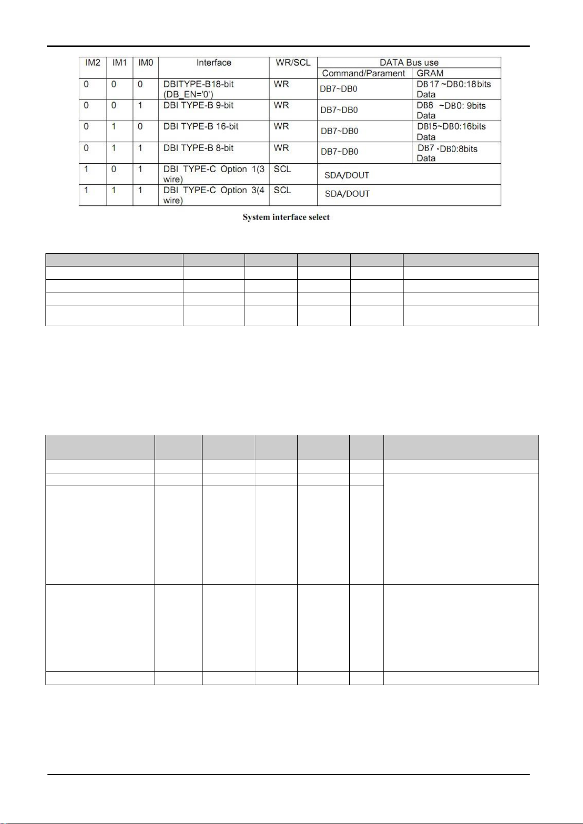
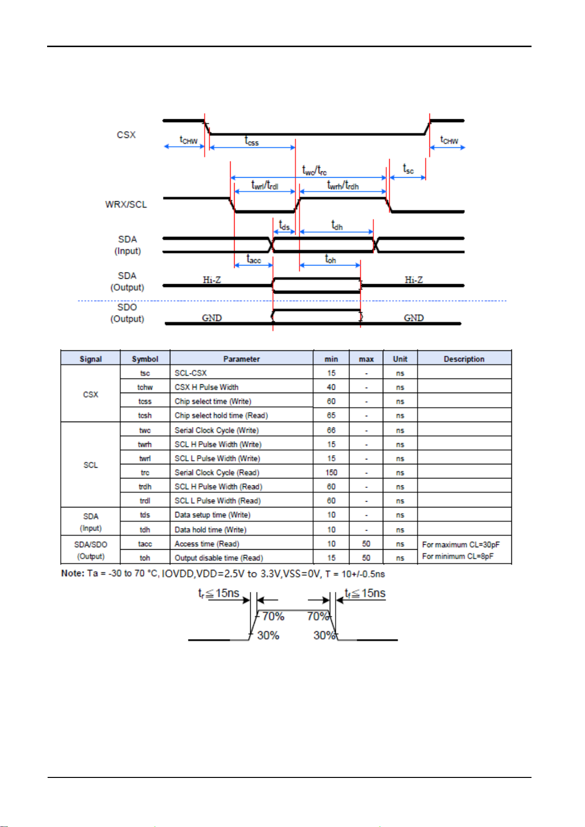
4. AC Characteristics
4.1 DBI Type B
4.1.1 DBI Type B Timing Characteristic
LEDK1
LEDA
LEDK6
:


TOPWAY
LCD Module User Manual
LMT035DNJFWD-NNA-1
URL: www.topwaydisplay.com
Document Name: LMT035DNJFWD-NNA-1-Manual-Rev0.2.doc
Page: 11 of 24
Please refer to IC: ILI9488 data sheet for more details.
4.2 3-Line SPI Interface Timing Characteristic
Please refer to IC: ILI9488 data sheet for more details.

TOPWAY
LCD Module User Manual
LMT035DNJFWD-NNA-1
URL: www.topwaydisplay.com
Document Name: LMT035DNJFWD-NNA-1-Manual-Rev0.2.doc
Page: 12 of 24
4.3 4-Line SPI Interface Timing Characteristic
Note:Ta=-30 to 70℃,IOVDD,VDD=2.5V to 3.3V,VSS=0V,T=10+/-0.5ns.
Please refer to IC: ILI9488 data sheet for more details.


TOPWAY
LCD Module User Manual
LMT035DNJFWD-NNA-1
URL: www.topwaydisplay.com
Document Name: LMT035DNJFWD-NNA-1-Manual-Rev0.2.doc
Page: 14 of 24
4.4.2 DPI Interface pixel format
The Pixel clock (DCLK) runs all the time without stop. It is used to enter VS, HS, DE and D[17: 0] states
when there is a rising edge of the DCLK. The DCLK cannot be used as the internal clock for other functions of
the display module.
Vertical synchronization (VS) is used to indicate when a new frame of the display is received. This is low
enable and its state is read to the display module by a rising edge of the DCLK signal.
Horizontal synchronization (HS) IS used to indicate when a new line of the frame is received. This is low
enable and its state is read to the display module by a rising edge of the DCLK signal.
Data Enable (DE) is used to indicate when the RGB information that should be transferred in the display is
received. This is a high enable, and its state is read to the display module by a rising edge of the DCLK signal.
D[17:0] is used to indicate what is the information of the image that is transferred on the display (when DE = 0
(low) and there is a rising edge of DCLK). D[17:0] can be 0(low) or 1(high). These lines are read by a rising
edge of the DCLK signal. In RGB interface modes, the input display data is written to GRAM first then outputs
the corresponding source voltage according to the gray data from GRAM.
Note:Please refer to IC: ILI9488 data sheet for more details.


TOPWAY
LCD Module User Manual
LMT035DNJFWD-NNA-1
URL: www.topwaydisplay.com
Document Name: LMT035DNJFWD-NNA-1-Manual-Rev0.2.doc
Page: 17 of 24
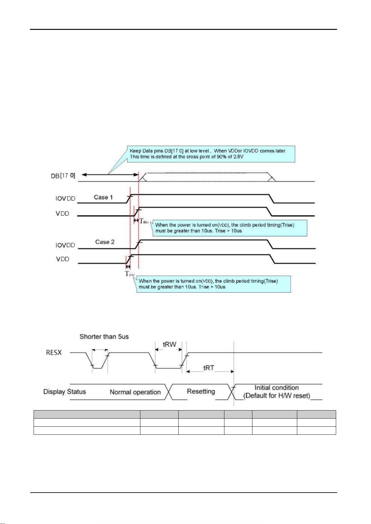
IOVDD and VDD can be applied or powered down in any order. During the Power Off sequence ,if the LCD is
in the Sleep In mode, VDD and IOVDD must be powered down with a minimum of 120 msec.If the LCD is in
the Sleep In mode, VDD and IOVDD can be powered down with a minimum of 0msec after the /RST has
been released. /CS can be applied at any time or can be permanently grounded. /RST has priority over /CS.
Notes:
1. There will be no damage to the ILI9488 if the power sequences are not met.
2. There will be no abnormal visible effects on the display panel during the Power On/Off Sequence.
3. There will be no abnormal visible effects on the display between the end of the Power On Sequence and before receiving the Sleep
Out command, and also between receiving the Sleep In command and the Power Off Sequence.
4. If the /RST line is not steadily held by the host during the Power On Sequence as defined in Sections 11.1 and 11.2 ( ILI9488
datasheet ), then it will be necessary to apply the Hardware /RST after the completion of the Host Power On Sequence to ensure
correct operations. Otherwise, all the functions are not guaranteed.
5. When the power is turned on, the climb period timing (Trise) must be greater than 10us.
6. Keep data pins D[17:0] at low level, or IOVDD comes later
Note:Please refer to IC: ILI9488 data sheet for more details.
4.6 Reset timing
Item
Symbol
MIN.
TYP.
MAX.
Unit
Reset LOW pulse width
tRW
1.0
-
-
us
Reset time
TRT
-
-
120
ms
Please refer to IC: ILI9488 data sheet for more details.


Table of contents
Other Topway Monitor manuals


