TQ MBa57 Series User manual

MBa57xx
User's Manual
MBa57xx UM 0100
15.04.2020

User's Manual l MBa57xx UM 0100 l © 2020, TQ-Systems GmbH Page i
TABLE OF CONTENTS
1. ABOUT THIS MANUAL................................................................................................................................................................................1
1.1 Copyright and licence expenses.............................................................................................................................................................1
1.2 Registered trademarks...............................................................................................................................................................................1
1.3 Disclaimer ......................................................................................................................................................................................................1
1.4 Imprint............................................................................................................................................................................................................1
1.5 Tips on safety................................................................................................................................................................................................2
1.6 Symbols and typographic conventions ...............................................................................................................................................2
1.7 Handling and ESD tips...............................................................................................................................................................................2
1.8 Naming of signals........................................................................................................................................................................................3
1.9 Further applicable documents / presumed knowledge .................................................................................................................3
2. BRIEF DESCRIPTION ....................................................................................................................................................................................4
3. TECHNICAL DATA........................................................................................................................................................................................4
3.1 System architecture and functionality..................................................................................................................................................4
3.1.1 MBa57xx Block diagram............................................................................................................................................................................4
3.1.2 Functionality.................................................................................................................................................................................................5
4. ELECTRONICS................................................................................................................................................................................................7
4.1 System components...................................................................................................................................................................................7
4.1.1 TQMa57xx......................................................................................................................................................................................................7
4.1.1.1 Overview TQMa57xx ..................................................................................................................................................................................7
4.1.1.2 TQMa57xx connectors...............................................................................................................................................................................7
4.1.1.3 Pinout TQMa57xx........................................................................................................................................................................................8
4.1.2 I2C address mapping ............................................................................................................................................................................... 12
4.1.3 Temperature sensor ................................................................................................................................................................................ 13
4.1.4 RTC backup................................................................................................................................................................................................. 13
4.1.5 Port Expander............................................................................................................................................................................................ 14
4.1.6 Power Management and Reset............................................................................................................................................................ 15
4.1.7 Power supply............................................................................................................................................................................................. 17
4.1.7.1 Protective circuitry................................................................................................................................................................................... 18
4.1.7.2 Power consumption................................................................................................................................................................................ 18
4.1.7.3 Power supply connectors ...................................................................................................................................................................... 18
4.2 Communication interfaces.................................................................................................................................................................... 19
4.2.1 USB 3.0 Super-Speed Host..................................................................................................................................................................... 19
4.2.2 USB 2.0 Hi-Speed Host............................................................................................................................................................................ 21
4.2.3 USB 2.0 Hi-Speed OTG ............................................................................................................................................................................ 22
4.2.4 Ethernet 10/100/1000BASE-T............................................................................................................................................................... 23
4.2.5 CAN............................................................................................................................................................................................................... 24
4.2.6 RS-485.......................................................................................................................................................................................................... 25
4.2.7 Debug interfaces...................................................................................................................................................................................... 26
4.2.8 LVDS ............................................................................................................................................................................................................. 27
4.2.9 Audio............................................................................................................................................................................................................ 30
4.2.10 SD card......................................................................................................................................................................................................... 31
4.2.11 PCIe............................................................................................................................................................................................................... 32
4.2.12 Mini PCIe ..................................................................................................................................................................................................... 34
4.2.13 SIM card....................................................................................................................................................................................................... 36
4.2.14 SATA............................................................................................................................................................................................................. 36
4.2.15 HDMI ............................................................................................................................................................................................................ 38
4.2.16 100 mil headers......................................................................................................................................................................................... 39
4.3 Diagnostic- and user interfaces ........................................................................................................................................................... 46
4.3.1 Diagnostic LEDs........................................................................................................................................................................................ 46
4.3.2 Push buttons.............................................................................................................................................................................................. 47
4.3.3 Buzzer........................................................................................................................................................................................................... 47
4.3.4 Power-On and Reset push button....................................................................................................................................................... 47
4.3.5 CAN and RS-485 termination................................................................................................................................................................ 47
4.3.6 Boot-Mode configuration...................................................................................................................................................................... 48
4.3.7 JTAG.............................................................................................................................................................................................................. 49

User's Manual l MBa57xx UM 0100 l © 2020, TQ-Systems GmbH Page ii
TABLE OF CONTENTS (continued)
5. SOFTWARE.................................................................................................................................................................................................. 50
6. MECHANICS................................................................................................................................................................................................ 50
6.1 Dimensions................................................................................................................................................................................................. 50
6.2 Thermal management ............................................................................................................................................................................ 50
6.3 Assembly..................................................................................................................................................................................................... 51
7. SAFETY REQUIREMENTS AND PROTECTIVE REGULATIONS......................................................................................................... 52
7.1 EMC............................................................................................................................................................................................................... 52
7.2 ESD................................................................................................................................................................................................................ 52
7.3 Operational safety and personal security......................................................................................................................................... 52
8. CLIMATIC AND OPERATIONAL CONDITIONS................................................................................................................................... 52
8.1 Protection against external effects..................................................................................................................................................... 52
8.2 Reliability and service life....................................................................................................................................................................... 52
9. ENVIRONMENT PROTECTION................................................................................................................................................................ 53
9.1 RoHS............................................................................................................................................................................................................. 53
9.2 WEEE®.......................................................................................................................................................................................................... 53
9.3 REACH®........................................................................................................................................................................................................ 53
9.4 EuP................................................................................................................................................................................................................ 53
9.5 Packaging ................................................................................................................................................................................................... 53
9.6 Batteries ...................................................................................................................................................................................................... 53
9.6.1 General notes ............................................................................................................................................................................................ 53
9.6.2 Lithium batteries ...................................................................................................................................................................................... 53
9.7 Other entries.............................................................................................................................................................................................. 53
10. APPENDIX ................................................................................................................................................................................................... 54
10.1 Acronyms and definitions...................................................................................................................................................................... 54
10.2 References.................................................................................................................................................................................................. 56

User's Manual l MBa57xx UM 0100 l © 2020, TQ-Systems GmbH Page iii
TABLE DIRECTORY
Table 1: Terms and Conventions..............................................................................................................................................................2
Table 2: Overview interfaces.....................................................................................................................................................................5
Table 3: Overview diagnostic and user’s interfaces...........................................................................................................................6
Table 4: Pinout connector X1, (TQMa57xx: X1) ...................................................................................................................................8
Table 5: Pinout connector X2, (TQMa57xx: X2) ...................................................................................................................................9
Table 6: Pinout connector X3, (TQMa57xx: X3) ................................................................................................................................ 10
Table 7: Pinout connector X4, (TQMa57xx: X4) ................................................................................................................................ 11
Table 8: I2C signals..................................................................................................................................................................................... 12
Table 9: I2C4 address assignment ........................................................................................................................................................ 12
Table 10: RTC backup supply.................................................................................................................................................................... 13
Table 11: Functions of port expanders.................................................................................................................................................. 14
Table 12: Functions of power signals..................................................................................................................................................... 15
Table 13: Functions of Reset signals....................................................................................................................................................... 16
Table 14: Voltages at MBa57xx headers................................................................................................................................................ 17
Table 15: Characteristics of protective circuit ..................................................................................................................................... 18
Table 16: Power supply connectors........................................................................................................................................................ 18
Table 17: Pinout X31, USB 3.0 Host1&2, Type A.................................................................................................................................. 20
Table 18: Pinout X32, USB 3.0 Host3, Micro B...................................................................................................................................... 20
Table 19: Pinout X55, USB 2.0 Host1 ...................................................................................................................................................... 21
Table 20: Pinout X56, USB 2.0 Host2 ...................................................................................................................................................... 21
Table 21: Pinout X26, USB 2.0 Host3 ...................................................................................................................................................... 21
Table 22: Pinout X29, USB 2.0 Host4 ...................................................................................................................................................... 21
Table 23: Pinout USB OTG, USB Micro AB, X9...................................................................................................................................... 22
Table 24: Pinout CAN1, CAN2................................................................................................................................................................... 24
Table 25: CAN termination, DIP switches S3, S7................................................................................................................................. 24
Table 26: Pinout RS-485, X7 ...................................................................................................................................................................... 25
Table 27: RS-485 termination, DIP switch S5....................................................................................................................................... 25
Table 28 Pinout Debug RS-232, X8........................................................................................................................................................ 26
Table 29 Pinout Debug USB, X10........................................................................................................................................................... 26
Table 30: Debug interface, DIP switch S6 ............................................................................................................................................. 26
Table 31: Type of LVDS connectors ........................................................................................................................................................ 27
Table 32: Pinout LVDS, X54....................................................................................................................................................................... 28
Table 33: Pinout LVDS CMD, X55............................................................................................................................................................. 29
Table 34: Configuration Line-Out / headphone ................................................................................................................................. 30
Table 35: Pinout Line-Out, X16 ................................................................................................................................................................ 30
Table 36: Pinout Line-In, X17.................................................................................................................................................................... 30
Table 37: Pinout Microphone, X18.......................................................................................................................................................... 30
Table 38: Pinout SD card, X14................................................................................................................................................................... 31
Table 39: Maximum currents, PCIe ......................................................................................................................................................... 32
Table 40: Pinout PCIe, X41......................................................................................................................................................................... 33
Table 41: Maximum currents, Mini PCIe................................................................................................................................................ 34
Table 42: Pinout Mini PCIe, X29............................................................................................................................................................... 35
Table 43: Pinout SIM card, X25................................................................................................................................................................. 36
Table 44: Pinout SATA, X26....................................................................................................................................................................... 37
Table 45: Pinout HDMI, X27 ...................................................................................................................................................................... 38
Table 46: Pinout 10/100 Mbit Ethernet ports, header X13, X12..................................................................................................... 39
Table 47: Pinout header X37, X36 ........................................................................................................................................................... 40
Table 48: Pinout header X45, X44 ........................................................................................................................................................... 41
Table 49: Pinout header X47, X46 ........................................................................................................................................................... 42
Table 50: Pinout header X49, X48 ........................................................................................................................................................... 43
Table 51: Pinout GPMC bus, header X51, X50..................................................................................................................................... 44
Table 52: Pinout header X56..................................................................................................................................................................... 45
Table 53: Diagnostic LEDs ......................................................................................................................................................................... 46
Table 54: Boot-Mode configuration, DIP switches S1, S2................................................................................................................ 48
Table 55: JTAG, DIP switch S13 ................................................................................................................................................................ 49
Table 56: Pinout JTAG, X11........................................................................................................................................................................ 49
Table 57: Labels on MBa57xx ................................................................................................................................................................... 51
Table 58: Climatic and operational conditions MBa57xx (without TQMa57xx)........................................................................ 52
Table 59: Acronyms ..................................................................................................................................................................................... 54
Table 60: Further applicable documents.............................................................................................................................................. 56

User's Manual l MBa57xx UM 0100 l © 2020, TQ-Systems GmbH Page iv
ILLUSTRATION DIRECTORY
Illustration 1: Block diagram MBa57xx with TQMa57xx..............................................................................................................................4
Illustration 2: Block diagram TQMa57xx ..........................................................................................................................................................7
Illustration 3: Block diagram I2C buses on TQMa57xx and MBa57xx ................................................................................................... 12
Illustration 4: Block diagram port expander D22 and D23...................................................................................................................... 14
Illustration 5: Block diagram Power................................................................................................................................................................ 15
Illustration 6: Block diagram Reset ................................................................................................................................................................. 16
Illustration 7: Block diagram power supply ................................................................................................................................................. 17
Illustration 8: Protective circuit for VIN ........................................................................................................................................................... 18
Illustration 9: Block diagram USB 3.0 Hosts ................................................................................................................................................. 19
Illustration 10: Block diagram USB 2.0 Hosts ................................................................................................................................................. 21
Illustration 11: Block diagram USB 2.0 Hi-Speed OTG................................................................................................................................. 22
Illustration 12: Block diagram Ethernet 10/100/1000BASE-T.................................................................................................................... 23
Illustration 13: Block diagram CAN ................................................................................................................................................................... 24
Illustration 14: Block diagram RS-485............................................................................................................................................................... 25
Illustration 15: Block diagram RS-232 / Debug.............................................................................................................................................. 26
Illustration 16: Block diagram LVDS.................................................................................................................................................................. 27
Illustration 17: Block diagram Audio ................................................................................................................................................................ 30
Illustration 18: Block diagram SD card............................................................................................................................................................. 31
Illustration 19: Block diagram PCIe ................................................................................................................................................................... 32
Illustration 20: Block diagram Mini PCIe.......................................................................................................................................................... 34
Illustration 21: Block diagram SATA.................................................................................................................................................................. 36
Illustration 22: Block diagram HDMI................................................................................................................................................................. 38
Illustration 23: Block diagram headers X12, X13, X36, X37, X44 ~ X51, X56 ........................................................................................ 39
Illustration 24: Block diagram push buttons.................................................................................................................................................. 47
Illustration 25: Block diagram buzzer............................................................................................................................................................... 47
Illustration 26: Block diagram Boot Mode DIP switches S1, S2 ................................................................................................................ 48
Illustration 27: Block diagram JTAG.................................................................................................................................................................. 49
Illustration 28: Component placement top.................................................................................................................................................... 51
Illustration 29: Component placement bottom............................................................................................................................................ 51
REVISION HISTORY
Revision Date Name Pos. Modification
0100 15.04.2020 Petz First edition

User's Manual l MBa57xx UM 0100 l © 2020, TQ-Systems GmbH Page 1
1. ABOUT THIS MANUAL
1.1 Copyright and licence expenses
Copyright protected © 2020 by TQ-Systems GmbH.
This User's Manual may not be copied, reproduced, translated, changed or distributed, completely or partially in electronic,
machine readable, or in any other form without the written consent of TQ-Systems GmbH.
The drivers and utilities for the components used as well as the BIOS are subject to the copyrights of the respective
manufacturers. The licence conditions of the respective manufacturer are to be adhered to.
Bootloader-licence expenses are paid by TQ-Systems GmbH and are included in the price.
Licence expenses for the operating system and applications are not taken into consideration and must be calculated / declared
separately.
1.2 Registered trademarks
TQ-Systems GmbH aims to adhere to copyrights of all graphics and texts used in all publications, and strives to use original
or license-free graphics and texts.
All brand names and trademarks mentioned in this User's Manual, including those protected by a third party, unless specified
otherwise in writing, are subjected to the specifications of the current copyright laws and the proprietary laws of the present
registered proprietor without any limitation. One should conclude that brand and trademarks are rightly protected by a third
party.
1.3 Disclaimer
TQ-Systems GmbH does not guarantee that the information in this User's Manual is up-to-date, correct, complete or of good
quality. Nor does TQ-Systems GmbH assume guarantee for further usage of the information. Liability claims against TQ-Systems
GmbH, referring to material or non-material related damages caused, due to usage or non-usage of the information given in this
User's Manual, or due to usage of erroneous or incomplete information, are exempted, as long as there is no proven intentional
or negligent fault of TQ-Systems GmbH.
TQ-Systems GmbH explicitly reserves the rights to change or add to the contents of this User's Manual or parts of it without
special notification.
Important Notice:
Before using the Starterkit MBa57xx or parts of the schematics of the MBa57xx, you must evaluate it and determine if it is suitable
for your intended application. You assume all risks and liability associated with such use. TQ-Systems GmbH makes no other
warranties including, but not limited to, any implied warranty of merchantability or fitness for a particular purpose. Except where
prohibited by law, TQ-Systems GmbH will not be liable for any indirect, special, incidental or consequential loss or damage
arising from the usage of the Starterkit MBa57xx or schematics used, regardless of the legal theory asserted.
1.4 Imprint
TQ-Systems GmbH
Gut Delling, Mühlstraße 2
D-82229 Seefeld
Tel: +49 8153 9308–0
Fax: +49 8153 9308–4223
E-Mail: Info@TQ-Group
Web: TQ-Group

User's Manual l MBa57xx UM 0100 l © 2020, TQ-Systems GmbH Page 2
1.5 Tips on safety
Improper or incorrect handling of the product can substantially reduce its life span.
1.6 Symbols and typographic conventions
Table 1: Terms and Conventions
Symbol Meaning
This symbol represents the handling of electrostatic-sensitive modules and / or components. These
components are often damaged / destroyed by the transmission of a voltage higher than about 50 V.
A human body usually only experiences electrostatic discharges above approximately 3,000 V.
This symbol indicates the possible use of voltages higher than 24 V.
Please note the relevant statutory regulations in this regard.
Non-compliance with these regulations can lead to serious damage to your health and also cause
damage / destruction of the component.
This symbol indicates a possible source of danger. Acting against the procedure described can lead to
possible damage to your health and / or cause damage / destruction of the material used.
This symbol represents important details or aspects for working with TQ-products.
Command
A font with fixed-width is used to denote commands, file names, or menu items.
1.7 Handling and ESD tips
General handling of your TQ-products
The TQ-product may only be used and serviced by certified personnel who have taken note of the
information, the safety regulations in this document and all related rules and regulations.
A general rule is: do not touch the TQ-product during operation. This is especially important when
switching on, changing jumper settings or connecting other devices without ensuring beforehand
that the power supply of the system has been switched off.
Violation of this guideline may result in damage / destruction of the MBa57xx and be dangerous
to your health.
Improper handling of your TQ-product would render the guarantee invalid.
Proper ESD handling
The electronic components of your TQ-product are sensitive to electrostatic discharge (ESD).
Always wear antistatic clothing, use ESD-safe tools, packing materials etc., and operate your TQ-
product in an ESD-safe environment. Especially when you switch modules on, change jumper settings,
or connect other devices.

User's Manual l MBa57xx UM 0100 l © 2020, TQ-Systems GmbH Page 3
1.8 Naming of signals
A hash mark (#) at the end of the signal name indicates a low-active signal.
Example: RESET#
If a signal can switch between two functions and if this is noted in the name of the signal, the low-active function is marked with
a hash mark and shown at the end.
Example: C / D#
If a signal has multiple functions, the individual functions are separated by slashes when they are important for the wiring.
The identification of the individual functions follows the above conventions.
Example: WE2# / OE#
1.9 Further applicable documents / presumed knowledge
•Specifications and manual of the modules used:
These documents describe the service, functionality and special characteristics of the module used (incl. BIOS).
•Specifications of the components used:
The manufacturer's specifications of the components used, for example CompactFlash cards, are to be taken note of.
They contain, if applicable, additional information that must be taken note of for safe and reliable operation.
These documents are stored at TQ-Systems GmbH.
•Chip errata:
It is the user’s responsibility to make sure all errata published by the manufacturer of each component are taken note of.
The manufacturer’s advice should be followed.
•Software behaviour:
No warranty can be given, nor responsibility taken for any unexpected software behaviour due to deficient components.
•General expertise:
Expertise in electrical engineering / computer engineering is required for the installation and the use of the device.
The following documents are required to fully comprehend the following contents:
•MBa57xx circuit diagram
•TQMa57xx User’s Manual
•AM57xx Reference Manuals
•U-Boot documentation: www.denx.de/wiki/U-Boot/Documentation
•Yocto documentation: www.yoctoproject.org/docs/
•TQ-Support Wiki: Support-Wiki TQMa57xx

User's Manual l MBa57xx UM 0100 l © 2020, TQ-Systems GmbH Page 4
2. BRIEF DESCRIPTION
This User's Manual describes the hardware of the MBa57xx Revision 02xx. The MBa57xx is designed as a carrier board for the
TQMa57xx. The illustrations in this User's Manual refer to the TQMa57xx. All interfaces provided by the TQMa57xx are available
on the MBa57xx. The function of the AM57xx can be evaluated, and therefore the software development for a TQMa57xx project
can start immediately. The MBa57xx supports all TQMa57xx modules with AM5718, AM5728, and AM5748 Single or Dual
Cortex®-A15 CPUs. More details may be taken from the AM57xx documentation, see Table 60.
3. TECHNICAL DATA
3.1 System architecture and functionality
3.1.1 MBa57xx Block diagram
Illustration 1: Block diagram MBa57xx with TQMa57xx

User's Manual l MBa57xx UM 0100 l © 2020, TQ-Systems GmbH Page 5
3.1.2 Functionality
Core of the system is the TQMa57xx with a TI AM57xx CPU. In addition to the standard communication interfaces like USB,
Ethernet, RS-232, RS-485, etc. all other available signals of the TQMa57xx are routed to 100 mil standard headers.
The MBa57xx provides the following interfaces and functions:
Table 2: Overview interfaces
Interface Qty. Connector Type Remark
USB 3.0 Super-Speed Host1&2 2 X31 USB, Type A Stacked
USB 3.0 Super-Speed Host3 1 X32 USB, Micro B –
USB 2.0 Hi-Speed Host1 1 X55 DF19, 20-pin LCD, LVDS
USB 2.0 Hi-Speed Host2 1 X56 100 mil header LCD, parallel, RGB
USB 2.0 Hi-Speed Host3 1 X26 M.2 Key-B SATA
USB 2.0 Hi-Speed Host4 1 X29 Mini PCIe –
USB 2.0 Hi-Speed OTG 1 X9 USB, Micro AB –
USB Debug 1 X10 USB, Micro AB –
Ethernet, Gbit 2 X52, X53 RJ45 2 × with integrated magnetics
Ethernet, 10/100 Base-T 2 X21 RJ45 Double, with integrated magnetics
CAN 2 X5, X6 Phoenix, 3-pin Galvanically separated
RS-485 1 X7 Phoenix, 5-pin Galvanically separated
RS-232 1 X8 D-Sub9 Debug UART
LVDS 1 X54 DF19, 30-pin LVDS data
LCD 1 X56 100 mil header LCD control signals, USB2.0,
resistive touch controller signals
HDMI 1.4 1 X27 HDMI –
Audio
1 X16
3.5 mm jacks
1 × Line-Out (stereo)
1 X17 1 × Line-In (stereo)
1 X18 1 × Mic (mono)
SD card 1 X14 Push-Pull –
SATA 1 X26 M.2 Key-B –
PCIe
1 X41 PCIe –
1 X29 Mini PCIe –
1 X25 SIM Card holder –
Headers 6 ×2
+ 1
X12/X13
X36/X37
X44/X45
X46/X47
X48/X49
X50/X51
X56
100 mil headers
Power-Out (12 V, 5 V, 3.3 V)
LCD interface (parallel)
Resistive Touch Controller
2× 10/100 Mbit Eth MII/MDIO
I2C, SPI, QSPI, GPIO, SDIO, GPMC bus
Power In 1 X23 DC jack (2.5 mm / 5.5 mm) VIN = 24 V DC ±5 %
1 X24 2-pin screw terminal block
Coin cell 1 X20 CR2032 holder Backup battery for RTC on TQMa57xx

User's Manual l MBa57xx UM 0100 l © 2020, TQ-Systems GmbH Page 6
3.1.2 Functionality (continued)
Table 3: Overview diagnostic and user’s interfaces
Interface Qty. Component Remark
Status-LEDs
8 Green LED
3 × VBUS USB3.0
1 × VBUS USB OTG
1 × VBUS (LVDS)
1 × VBUS (RGB)
1 × VBUS (SATA)
1 × VBUS (Mini PCIe)
3 Green LED Mini PCIe WWAN, WLAN, WPAN
2 Green LED GPIO LEDs at Port Expander II
1 Green LED SATA status
8 Green LED Power LEDs (24V, 12V, 5V, 3.3V, 3.3V-mPCIe, 1.8V, 1.5V, 1.1V)
1 Green LED Debug LEDs for USB debug interface
1 Green / red LED Reset LED
8 Green / yellow LED Ethernet-LEDs (Activity / Speed)
Power / Reset buttons 2 Push button CPU / PMIC reset, CPU-ONOFF
Push buttons 3 Push button Push buttons at I2C Port Expander I
Boot Mode configuration 2 DIP switch 2 × 8-fold Boot Device configuration
CAN and RS-485 termination 3 DIP switch 3 × 2-fold
Debug USB / RS-232 1 DIP switch 1 × single
Signal generator 1 Buzzer Connected to I2C Port Expander II
JTAG 1 20-pin header 100 mil

User's Manual l MBa57xx UM 0100 l © 2020, TQ-Systems GmbH Page 7
4. ELECTRONICS
4.1 System components
4.1.1 TQMa57xx
4.1.1.1 Overview TQMa57xx
Illustration 2: Block diagram TQMa57xx
Depending on the variant, the TQMa57xx features a Single or Dual Core Cortex®-A15 CPU with two Cortex®-M4 Image Processing
Units (IPU) and one or two C66x Digital Signal Processor (DSP) subsystems. It can be used for all three variants AM5718, AM5728
and AM5748. The maximum clock rate of the CPUs is 1.5 GHz, the DSPs can be clocked with up to 750 MHz. The AM574x supports
ECC and Secure Boot. More detailed information can be found in the TQMa57xx User's Manual (12).
4.1.1.2 TQMa57xx connectors
The available signals are routed to four connectors on the MBa57xx.
Note: TQMa57xx interfaces
Depending on the selected TQMa57xx, not all interfaces are available.
Available interfaces are to be taken from the TQMa57xx User’s Manual
or the pinout tables in chapter 4.1.1.3.
The pin assignments listed in Table 4 to Table 7 refer to the BSP provided by TQ-Systems GmbH.
User's Manual l MBa57xx UM 0100 l © 2020, TQ-Systems GmbH Page 8
4.1.1.3 Pinout TQMa57xx
Table 4: Pinout connector X1, (TQMa57xx: X1)
Ball Type Level Group Signal Pin Signal Group Level Type Ball
– P 0 V GND DGND 1 2 DGND GND 0 V P –
C9
O
1.8 V
LCD
VOUT1_D[20]
3
4
UART10_RTS#
UART
3.3 V
O
F4
A7
O
1.8 V
LCD
VOUT1_D[18]
5
6
UART10_RXD
UART
3.3 V
I
D1
B7
O
1.8 V
LCD
VOUT1_D[16]
7
8
UART10_TXD
UART
3.3 V
O
E2
C8
O
1.8 V
LCD
VOUT1_D[14]
9
10
DGND
GND
0 V
P
–
A5
O
1.8 V
LCD
VOUT1_D[12]
11
12
VOUT1_D[23]
LCD
1.8 V
O
A10
D7
O
1.8 V
LCD
VOUT1_D[10]
13
14
VOUT1_D[22]
LCD
1.8 V
O
B9
E8
O
1.8 V
LCD
VOUT1_D[8]
15
16
VOUT1_D[21]
LCD
1.8 V
O
A9
–
P
0 V
GND
DGND
17
18
VOUT1_D[19]
LCD
1.8 V
O
A8
F8
O
1.8 V
LCD
VOUT1_D[6]
19
20
VOUT1_D[17]
LCD
1.8 V
O
B8
G11
O
1.8 V
LCD
VOUT1_D[3]
21
22
VOUT1_D[15]
LCD
1.8 V
O
C7
F10
O
1.8 V
LCD
VOUT1_D[2]
23
24
VOUT1_D[13]
LCD
1.8 V
O
C6
G10
O
1.8 V
LCD
VOUT1_D[1]
25
26
DGND
GND
0 V
P
–
F11 O 1.8 V LCD VOUT1_D[0] 27 28 VOUT1_D[11] LCD 1.8 V O D8
B11
I/O
1.8 V
GPIO
VOUT1_FLD (GPIO4_21)
29
30
VOUT1_D[9]
LCD
1.8 V
O
D9
B10
O
1.8 V
LCD
VOUT1_DE
31
32
VOUT1_D[7]
LCD
1.8 V
O
E7
–
P
0 V
GND
DGND
33
34
VOUT1_D[5]
LCD
1.8 V
O
F9
D11
O
1.8 V
LCD
VOUT1_CLK
35
36
VOUT1_D[4]
LCD
1.8 V
O
E9
–
I
3.3 V
Config
RST_FROM_MB#
37
38
VOUT1_VSYNC
LCD
1.8 V
O
E11
–
O
3.3 V
Config
RST_TO_MB#
39
40
VOUT1_HSYNC
LCD
1.8 V
O
C11
D20
I
3.3 V
JTAG
JTAG_TRSTN
41
42
DGND
GND
0 V
P
–
F18
I
3.3 V
JTAG
JTAG_TMS
43
44
GPIO4_0_G6
GPIO
3.3 V
I/O
G6
F19
O
3.3 V
JTAG
JTAG_TDO
45
46
GPIO4_1_F2 (PMIC_INT)
Config
3.3 V
I
F2
D23 I 3.3 V JTAG JTAG_TDI 47 48 GPIO4_2_F3 (TEMP_INT#) Config 3.3 V I F3
–
P
0 V
GND
DGND
49
50
GPIO4_5_D2
GPIO
3.3 V
I/O
D2
E20
I
3.3 V
JTAG
JTAG_TCLK
51
52
GPIO5_1_J14
GPIO
3.3 V
I/O
J14
E18
O
3.3 V
JTAG
JTAG_RTCK
53
54
USB2.0_OTG_OC#
USB
3.3 V
I
G13
D24
I/O
3.3 V
JTAG
JTAG_EMU1
55
56
GPIO5_5_J11
GPIO
3.3 V
I/O
J11
G21
I/O
3.3 V
JTAG
JTAG_EMU0
57
58
DGND
GND
0 V
P
–
–
P
0 V
GND
DGND
59
60
MCASP8_ACLKX
AUDIO
3.3 V
I/O
B17
E12
I/O
3.3 V
GPIO
GPIO5_6_E12
61
62
MCASP8_FSX
AUDIO
3.3 V
I/O
A17
F13
I/O
3.3 V
GPIO
GPIO5_7_F13
63
64
MCASP8_AXR[0]
AUDIO
3.3 V
I/O
D15
C12
I/O
3.3 V
GPIO
GPIO5_8_C12
65
66
MCASP8_AXR[1]
AUDIO
3.3 V
I/O
B16
D12
I/O
3.3 V
GPIO
GPIO5_9_D12
67
68
MCASP8_AXR[2]
AUDIO
3.3 V
I/O
E15
–
P
0 V
GND
DGND
69
70
MCASP8_AXR[3]
AUDIO
3.3 V
I/O
A20
C18
I/O
3.3 V
AUDIO
MCASP4_C18
71
72
MCASP8_AHCLKX
AUDIO
3.3 V
O
C23
A15 I/O 3.3 V AUDIO MCASP2_A15 73 74 DGND GND 0 V P –
F22
I
3.3 V
Config
AM57XX_PORZ#
75
76
DCAN1_RX
CAN
3.3 V
I
G19
F23
O
3.3 V
Config
RSTOUT#
77
78
DCAN1_TX
CAN
3.3 V
O
G20
E23
I
3.3 V
Config
RESET#
79
80
DGND
GND
0 V
P
–
–
P
0 V
GND
DGND
81
82
DCAN2_RX
CAN
3.3 V
I
F20
A22
O
3.3 V
SATA
SATA1_LED
83
84
DCAN2_TX
CAN
3.3 V
O
E21
B15
I/O
3.3 V
AUDIO
MCASP2_B15
85
86
DGND
GND
0 V
P
–
–
O
5 V
Config
PMIC_REGEN1
87
88
I2C4_SDA
I2C
3.3 V
I/O
B14
B20
I/O
3.3 V
HDMI
HDMI1_CEC
89
90
I2C4_SCL
I2C
3.3 V
O
A21
B21
I
3.3 V
HDMI
HDMI1_HPD
91
92
DGND
GND
0 V
P
–
F17
I/O
3.3 V
HDMI
HDMI1_DDC_SDA
93
94
I2C5_SDA
I2C
3.3 V
I/O
AA3
C25
O
3.3 V
HDMI
HDMI1_DDC_SCL
95
96
I2C5_SCL
I2C
3.3 V
O
AB9
–
P
0 V
GND
DGND
97
98
DGND
GND
0 V
P
–
G17
I/O
3.3 V
GPIO
GPIO7_16_G17
99
100
UART3_RXD
UART
3.3 V
I
A26
B24
I/O
3.3 V
GPIO
GPIO7_17_B24
101
102
UART3_TXD
UART
3.3 V
O
B22
D28
I/O
3.3 V
SDIO
MMC4_DAT[0]
103
104
DGND
GND
0 V
P
–
D26
I/O
3.3 V
SDIO
MMC4_DAT[1]
105
106
UART4_RXD
UART
3.3 V
I
G16
D27
I/O
3.3 V
SDIO
MMC4_DAT[2]
107
108
UART4_TXD
UART
3.3 V
O
D17
C28
I/O
3.3 V
SDIO
MMC4_DAT[3]
109
110
DGND
GND
0 V
P
–
C26
I
3.3 V
SDIO
MMC4_SDWP
111
112
UART8_RTS#
UART
3.3 V
O
AH6
–
P
0 V
GND
DGND
113
114
UART8_RXD
UART
3.3 V
I
AE8
E25
O
3.3 V
SDIO
MMC4_CLK
115
116
UART8_TXD
UART
3.3 V
O
AD8
C27
I/O
3.3 V
SDIO
MMC4_CMD
117
118
GPIO3_28_E1
GPIO
3.3 V
I/O
E1
B27
I
3.3 V
SDIO
MMC4_SDCD
119
120
DGND
GND
0 V
P
–
User's Manual l MBa57xx UM 0100 l © 2020, TQ-Systems GmbH Page 9
4.1.1.3 Pinout TQMa57xx (continued)
Table 5: Pinout connector X2, (TQMa57xx: X2)
Ball Type Level Group Signal Pin Signal Group Level Type Ball
– P 5 V Power VDD5V 1 2 VDD5V Power 5 V P –
–
P
5 V
Power
VDD5V
3
4
VDD5V
Power
5 V
P
–
– P 5 V Power VDD5V 5 6 VDD5V Power 5 V P –
– P 5 V Power VDD5V 7 8 VDD5V Power 5 V P –
– P 0 V GND DGND 9 10 VDD5V Power 5 V P –
– P 0 V GND DGND 11 12 DGND GND 0 V P –
– P 3.3 V BAT V_BAT 13 14 DGND GND 0 V P –
– P 0 V GND DGND 15 16 DGND GND 0 V P –
F6 I/O 3.3 V ENET PR1_MDIO_DATA /
GMAC_MDIO_DATA 17 18 WAKEUP0 Config 3.3 V I AD17
D3 O 3.3 V ENET PR1_MDIO_MDCLK /
GMAC_MDIO_MCLK 19 20 GPIO3_29_G2 GPIO 3.3 V I/O G2
– P 0 V GND DGND 21 22 PR1_MII1_TXEN ENET 3.3 V O E4
A4 I 3.3 V ENET PR1_MII1_CRS /
RGMII1_RXD0 23 24 PR1_MII1_MT_CLK ENET 3.3 V I C1
B5 I 3.3 V ENET PR1_MII1_COL /
RGMII1_RXD1 25 26 DGND GND 0 V P –
B4 I 3.3 V ENET PR1_MII1_RXLINK /
RGMII1_RXD2
27 28 PR1_MII1_TXD1 /
RGMII1_TXC
ENET 3.3 V O D5
B3 I 3.3 V ENET PR1_MII1_RXER /
RGMII1_RXD3 29 30 PR1_MII1_TXD0 /
RGMII1_TXCTL ENET 3.3 V O C2
– P 0 V GND DGND 31 32 PR1_MII1_TXD2 ENET 3.3 V O E6
D6 I/O 3.3 V ENET PR1_MII1_RXD2 /
RGMII1_TXD0 33 34 PR1_MII1_TXD3 ENET 3.3 V O F5
B2 I/O 3.3 V ENET PR1_MII1_RXD3 /
RGMII1_TXD1 35 36 PR1_MII1_RXD0 /
RGMII1_RXCTL ENET 3.3 V I A3
C4 I/O 3.3 V ENET PR1_MII1_RXDV /
RGMII1_TXD2 37 38 PR1_MII1_RXD1 /
RGMII1_RXC ENET 3.3 V I C5
C3 I/O 3.3 V ENET PR1_MII1_MR_CLK /
RGMII1_TXD3 39 40 DGND GND 0 V P –
– I 5 V USB VUSB_VBUS2 41 42 GPIO3_30_H7 GPIO 3.3 V I/O H7
– I 5 V Config PMIC_PWRON# 43 44 PR2_MDIO_DATA ENET 3.3 V I/O D14
K14 I 1.8 V Config E–FUSE_1V8 45 46 PR2_MDIO_MDCLK ENET 3.3 V O C14
– P 0 V GND DGND 47 48 DGND GND 0 V P –
A13 I 3.3 V ENET PR2_MII0_MR_CLK 49 50 PR2_MII0_MT_CLK ENET 3.3 V I F12
G12 I 3.3 V ENET PR2_MII0_RXER 51 52 PR2_MII0_TXEN ENET 3.3 V O B12
C15 I 3.3 V ENET PR2_MII0_RXD[0] 53 54 PR2_MII0_TXD[0] ENET 3.3 V O E14
A18 I 3.3 V ENET PR2_MII0_RXD[1] 55 56 DGND GND 0 V P –
A19 I 3.3 V ENET PR2_MII0_RXD[2] 57 58 PR2_MII0_TXD[1] ENET 3.3 V O A12
F14 I 3.3 V ENET PR2_MII0_RXD[3] 59 60 PR2_MII0_TXD[2] ENET 3.3 V O B13
– P 0 V GND DGND 61 62 PR2_MII0_TXD[3] ENET 3.3 V O A11
G14 I 3.3 V ENET PR2_MII0_RXDV 63 64 PR2_MII0_COL ENET 3.3 V I F15
A16 I 3.3 V ENET PR2_MII0_RXLINK 65 66 PR2_MII0_CRS ENET 3.3 V I B18
F21 I/O 3.3 V GPIO GPIO6_16_F21 67 68 DGND GND 0 V P –
B26 I/O 3.3 V GPIO GPIO6_19_B26 69 70 PR2_MII1_RXLINK ENET 3.3 V I C17
B25 I/O 3.3 V SPI SPI1_D0 71 72 PR2_MII1_CRS ENET 3.3 V I E17
F16
I/O
3.3 V
SPI
SPI1_D1
73
74
PR2_MII1_COL
ENET
3.3 V
I
D18
– P 0 V GND DGND 75 76 GPIO3_1_AF9 GPIO 3.3 V I/O AF9
A25 O 3.3 V SPI SPI1_SCLK 77 78 NMIN_DSP Config 3.3 V I D21
A24 O 3.3 V SPI SPI1_CS0 79 80 DGND GND 0 V P –
User's Manual l MBa57xx UM 0100 l © 2020, TQ-Systems GmbH Page 10
4.1.1.3 Pinout TQMa57xx (continued)
Table 6: Pinout connector X3, (TQMa57xx: X3)
Ball Type Level Group Signal Pin Signal Group Level Type Ball
N6 O 1.8 V GPMC GPMC_BE#[0] (GPIO2_26) 1 2 DGND GND 0 V P –
M4
O
1.8 V
GPMC
GPMC_BE#[1] (GPIO2_27)
3
4
GPMC_CLK (GPIO2_22)
GPMC
1.8 V
O
P7
M6 I/O 1.8 V Boot/GPMC GPMC_AD[0] (GPIO1_6) 5 6 GPMC_CS0 (GPIO2_19) GPMC 1.8 V O T1
M2 I/O 1.8 V Boot/GPMC GPMC_AD[1] (GPIO1_7) 7 8 GPMC_OE#_RE# (GPIO2_24) GPMC 1.8 V O M5
– P 0 V GND DGND 9 10 GPMC_WE# (GPIO2_25) GPMC 1.8 V O M3
L5 I/O 1.8 V Boot/GPMC GPMC_AD[2] (GPIO1_8) 11 12 GPMC_ADV#_ALE
(GPIO2_23)
GPMC 1.8 V O N1
M1 I/O 1.8 V Boot/GPMC GPMC_AD[3] (GPIO1_9) 13 14 GPMC_A[1] (GPIO7_4) GPMC 1.8 V O T9
L6 I/O 1.8 V Boot/GPMC GPMC_AD[4] (GPIO1_10) 15 16 GPMC_A[2] (GPIO7_5) GPMC 1.8 V O T6
L4 I/O 1.8 V Boot/GPMC GPMC_AD[5] (GPIO1_11) 17 18 DGND GND 0 V P –
L3 I/O 1.8 V Boot/GPMC GPMC_AD[6] (GPIO1_12) 19 20 GPMC_A[3] (GPIO7_6) GPMC 1.8 V O T7
L2 I/O 1.8 V Boot/GPMC GPMC_AD[7] (GPIO1_13) 21 22 GPMC_A[4] (GPIO1_26) GPMC 1.8 V O P6
L1 I/O 1.8 V Boot/GPMC GPMC_AD[8] (GPIO7_18) 23 24 GPMC_A[5] (GPIO1_27) GPMC 1.8 V O R9
– P 0 V GND DGND 25 26 GPMC_A[6] (GPIO1_28) GPMC 1.8 V O R5
K2 I/O 1.8 V Boot/GPMC GPMC_AD[9] (GPIO7_19) 27 28 GPMC_A[7] (GPIO1_29) GPMC 1.8 V O P5
J1 I/O 1.8 V Boot/GPMC GPMC_AD[10] (GPIO7_28) 29 30 GPMC_A[8] (GPIO1_30) GPMC 1.8 V O N7
J2 I/O 1.8 V Boot/GPMC GPMC_AD[11] (GPIO7_29) 31 32 GPMC_A[9] (GPIO1_31) GPMC 1.8 V O R4
H1
I/O
1.8 V
Boot/GPMC
GPMC_AD[12] (GPIO1_18)
33
34
DGND
GND
0 V
P
–
J3 I/O 1.8 V Boot/GPMC GPMC_AD[13] (GPIO1_19) 35 36 GPMC_A[10] (GPIO2_0) GPMC 1.8 V O N9
H2 I/O 1.8 V Boot/GPMC GPMC_AD[14] (GPIO1_20) 37 38 GPMC_A27_AF4 (GPIO3_19) GPMC 3.3 V O AF4
H3 I/O 1.8 V Boot/GPMC GPMC_AD[15] (GPIO1_21) 39 40 GPMC_A27_G1 (GPIO3_31) GPMC 3.3 V O G1
AD9 I/O 3.3 V GPIO GPIO3_0_AD9 41 42 DGND GND 0 V P –
B19 I 3.3 V ENET PR2_MII1_RXER 43 44 PR1_MII0_MT_CLK /
RGMII0_RXC ENET 3.3 V I U5
–
P
0 V
GND
DGND
45
46
PR1_MII0_COL (GPIO5_15)
ENET
3.3 V
I
V1
Y1 I 3.3 V ENET PR1_MII0_MR_CLK
(GPIO5_19) 47 48 PR1_MII0_TXD3 /
RGMII0_RXCTL ENET 3.3 V I/O V5
V2 I 3.3 V ENET PR1_MII0_RXDV (GPIO5_18) 49 50 DGND GND 0 V P –
U7 I/O 3.3 V ENET PR1_MII0_RXER /
RGMII0_TXD2 51 52 PR1_MII0_TXD0 /
RGMII0_RXD0 ENET 3.3 V I/O W2
V7 I/O 3.3 V ENET PR1_MII0_CRS /
RGMII0_TXD3 53 54 PR1_MII0_TXD1 /
RGMII0_RXD1 ENET 3.3 V I/O Y2
U6 I/O 3.3 V ENET PR1_MII0_RXD0 /
RGMII0_TXD0 55 56 PR1_MII0_TXD2 /
RGMII0_RXD3 ENET 3.3 V I/O V4
V6 I/O 3.3 V ENET PR1_MII0_RXD1 /
RGMII0_TXD1 57 58 PR1_MII0_TXEN /
RGMII0_RXD2 ENET 3.3 V I/O V3
– P 0 V GND DGND 59 60 DGND GND 0 V P –
W9 I/O 3.3 V ENET PR1_MII0_RXD3 /
RGMII0_TXC 61 62 PR2_MII1_RXD[0] ENET 3.3 V I AB5
V9 I/O 3.3 V ENET PR1_MII0_RXD2 /
RGMII0_TXCTL 63 64 PR2_MII1_RXD[1] ENET 3.3 V I AB8
U4 I 3.3 V ENET PR1_MII0_RXLINK
(GPIO5_16) 65 66 PR2_MII1_RXD[2] ENET 3.3 V I AD6
– P 0 V GND DGND 67 68 PR2_MII1_RXD[3] ENET 3.3 V I AC8
U3 I/O 3.3 V ENET RMII_MHZ_50_CLK 69 70 PR2_MII1_TXEN ENET 3.3 V O AB4
– P 0 V GND DGND 71 72 PR2_MII1_TXD[0] ENET 3.3 V O AC6
AC9
I
3.3 V
ENET
PR2_MII1_MR_CLK
73
74
PR2_MII1_TXD[1]
ENET
3.3 V
O
AC7
AC3 I 3.3 V ENET PR2_MII1_RXDV 75 76 PR2_MII1_TXD[2] ENET 3.3 V O AC4
AC5 I 3.3 V ENET PR2_MII1_MT_CLK 77 78 PR2_MII1_TXD[3] ENET 3.3 V O AD4
– P 0 V GND DGND 79 80 DGND GND 0 V P –

User's Manual l MBa57xx UM 0100 l © 2020, TQ-Systems GmbH Page 11
4.1.1.3 Pinout TQMa57xx (continued)
Table 7: Pinout connector X4, (TQMa57xx: X4)
Ball Type Level Group Signal Pin Signal Group Level Type Ball
– P 0 V GND DGND 1 2 USB3.0_DRVVBUS USB 3.3 V O AB10
AC12
I/O
3.3 V
USB
USB3.0_DM
3
4
DGND
GND
0 V
P
–
AD12
I/O
3.3 V
USB
USB3.0_DP
5
6
DGND
GND
0 V
P
–
–
P
0 V
GND
DGND
7
8
DGND
GND
0 V
P
–
AC11
O
1.8 V
USB
USB3.0_TXN0
9
10
USB3.0_RXP0
USB
1.8 V
I
AE12
AD11
O
1.8 V
USB
USB3.0_TXP0
11
12
USB3.0_RXN0
USB
1.8 V
I
AF12
–
P
0 V
GND
DGND
13
14
DGND
GND
0 V
P
–
AE11
I/O
3.3 V
USB
USB2.0_DP
15
16
USB2.0_DM
USB
3.3 V
I/O
AF11
AC16
I
3.3 V
USB
USB2.0_OTG_ID
17
18
USB2.0_DRVVBUS
USB
3.3 V
O
AC10
–
P
0 V
GND
DGND
19
20
DGND
GND
0 V
P
–
AH9
I
1.8 V
SATA
SATA1_RXN0
21
22
SATA1_TXN0
SATA
1.8 V
O
AG10
AG9
I
1.8 V
SATA
SATA1_RXP0
23
24
SATA1_TXP0
SATA
1.8 V
O
AH10
–
P
0 V
GND
DGND
25
26
DGND
GND
0 V
P
–
– P 0 V GND DGND 27 28 PCIE_RXN1 PCIE 1.8 V I AG11
–
P
0 V
GND
DGND
29
30
PCIE_RXP1
PCIE
1.8 V
I
AH11
AG13
I
1.8 V
PCIE
PCIE_RXN0
31
32
DGND
GND
0 V
P
–
AH13
I
1.8 V
PCIE
PCIE_RXP0
33
34
DGND
GND
0 V
P
–
–
P
0 V
GND
DGND
35
36
PCIE_TXN1
PCIE
1.8 V
O
AG12
–
P
0 V
GND
DGND
37
38
PCIE_TXP1
PCIE
1.8 V
O
AH12
AG15
I
1.8 V
PCIE
PCIE_CLKP
39
40
DGND
GND
0 V
P
–
AH15
I
1.8 V
PCIE
PCIE_CLKN
41
42
DGND
GND
0 V
P
–
–
P
0 V
GND
DGND
43
44
PCIE_TXN0
PCIE
1.8 V
O
AG14
–
P
0 V
GND
DGND
45
46
PCIE_TXP0
PCIE
1.8 V
O
AH14
AG16 O 1.8 V HDMI HDMI1_CLOCKX 47 48 DGND GND 0 V P –
AH16
O
1.8 V
HDMI
HDMI1_CLOCKY
49
50
DGND
GND
0 V
P
–
–
P
0 V
GND
DGND
51
52
DGND
GND
0 V
P
–
AG18
O
1.8 V
HDMI
HDMI1_DATA1X
53
54
HDMI1_DATA0X
HDMI
1.8 V
O
AG17
AH18
O
1.8 V
HDMI
HDMI1_DATA1Y
55
56
HDMI1_DATA0Y
HDMI
1.8 V
O
AH17
–
P
0 V
GND
DGND
57
58
DGND
GND
0 V
P
–
AH19
O
1.8 V
HDMI
HDMI1_DATA2Y
59
60
HDMI1_DATA2X
HDMI
1.8 V
O
AG19
–
P
0 V
GND
DGND
61
62
DGND
GND
0 V
P
–
R6
I/O
1.8 V
GPIO
GPIO7_3_R6
63
64
QSPI_SCK
QSPI
1.8 V
O
R2
Y9
I
3.3 V
SD
MMC1_SDWP
65
66
QSPI_RTCLK
QSPI
1.8 V
I
R3
–
P
0 V
GND
DGND
67
68
QSPI_SS1#
QSPI
1.8 V
O
P1
W6
O
3.3 V
SD
MMC1_CLK
69
70
DGND
GND
0 V
P
–
Y6
I/O
3.3 V
SD
MMC1_CMD
71
72
QSPI_DATA0
QSPI
1.8 V
I/O
U1
AA6 I/O 3.3 V SD MMC1_DAT[0] 73 74 QSPI_DATA1 QSPI 1.8 V I/O P3
Y4
I/O
3.3 V
SD
MMC1_DAT[1]
75
76
QSPI_DATA2
QSPI
1.8 V
I/O
U2
AA5
I/O
3.3 V
SD
MMC1_DAT[2]
77
78
QSPI_DATA3
QSPI
1.8 V
I/O
T2
Y3
I/O
3.3 V
SD
MMC1_DAT[3]
79
80
DGND
GND
0 V
P
–
W7
I
3.3 V
SD
MMC1_SDCD
81
82
QSPI_SS0#
QSPI
1.8 V
O
P2
–
P
0 V
GND
DGND
83
84
GPIO3_22_AE5
GPIO
3.3 V
I/O
AE5
AE9
I/O
3.3 V
GPIO
GPIO3_2_AE9
85
86
GPIO3_23_AE1
GPIO
3.3 V
I/O
AE1
AF8
I/O
3.3 V
GPIO
GPIO3_3_AF8
87
88
GPIO3_24_AE2
GPIO
3.3 V
I/O
AE2
–
P
0 V
GND
DGND
89
90
GPIO3_25_AE6
GPIO
3.3 V
I/O
AE6
AF6
I/O
3.3 V
GPIO
GPIO3_17_AF6
91
92
GPIO3_26_AD2
GPIO
3.3 V
I/O
AD2
AF3
I/O
3.3 V
GPIO
GPIO3_18_AF3
93
94
GPIO3_27_AD3
GPIO
3.3 V
I/O
AD3
AF1
I/O
3.3 V
GPIO
GPIO3_20_AF1
95
96
PR1_PRU0_GPO5_AG4
ENET
3.3 V
O
AG4
AE3
I/O
3.3 V
GPIO
GPIO3_21_AE3
97
98
DGND
GND
0 V
P
–
AG7
I/O
3.3 V
GPIO
GPIO3_6_AG7
99
100
PR1_PRU0_GPO6_AG2
ENET
3.3 V
O
AG2
AH3
I
3.3 V
ENET
PR1_PRU0_GPI1_AH3
101
102
PR1_PRU0_GPO7_AG3
ENET
3.3 V
O
AG3
AH5
I
3.3 V
ENET
PR1_PRU0_GPI2_AH5
103
104
PR1_PRU0_GPO8_AG5
ENET
3.3 V
O
AG5
–
P
0 V
GND
DGND
105
106
PR1_PRU0_GPO9_AF2
ENET
3.3 V
O
AF2
AG6
I
3.3 V
ENET
PR1_PRU0_GPI3_AG6
107
108
GPIO2_28_N2
GPIO
1.8 V
I/O
N2
AH4
I
3.3 V
ENET
PR1_PRU0_GPI4_AH4
109
110
GPIO2_30_AG8
GPIO
3.3 V
I/O
AG8
AC17
I/O
3.3 V
GPIO
GPIO1_1_AC17
111
112
GPIO2_31_AH7
GPIO
3.3 V
I/O
AH7
AB16
I/O
3.3 V
GPIO
GPIO1_2_AB16
113
114
DGND
GND
0 V
P
–
P9 I/O 1.8 V GPIO GPIO2_1_P9 115 116 MCASP5_AA4
(PR2_PRU1_GPO4)
AUDIO 3.3 V I/O AA4
P4 I/O 1.8 V GPIO GPIO2_2_P4 117 118 MCASP5_AB3
(PR2_PRU1_GPO3)
AUDIO 3.3 V I/O AB3
–
P
0 V
GND
DGND
119
120
DGND
GND
0 V
P
–

User's Manual l MBa57xx UM 0100 l © 2020, TQ-Systems GmbH Page 12
4.1.2 I2C address mapping
Illustration 3: Block diagram I2C buses on TQMa57xx and MBa57xx
The TQMa57xx offers two I2C interfaces, which are available on the TQMa57xx connectors as primary function.
I2C1 is a TQMa57xx internal I2C bus, which is exclusively used for the I2C devices on the TQMa57xx. This bus is not available.
The corresponding addresses can be taken from the User's Manual of the TQMa57xx (12).
I2C5 is routed to header X48 on the MBa57xx, no I2C devices are connected.
Further I2C interfaces can be provided by an adapted pin multiplexing.
The following table shows the signals used on the two I2C interfaces:
Table 8: I2C signals
Signal Direction MBa57xx Remark
I2C4_SDA I/O X1-88 2.7 kΩ PU to 3.3 V on MBa57xx
I2C4_SCL O X1-90 2.7 kΩ PU to 3.3 V on MBa57xx
I2C5_SDA I/O X1-94 2.7 kΩ PU to 3.3 V on MBa57xx
I2C5_SCL O X1-96 2.7 kΩ PU to 3.3 V on MBa57xx
The following table shows the I2C4 addresses used on the MBa57xx.
Table 9: I2C4 address assignment
Reference Device Usage 7-bit address
D22 PCA9555PW GPIO expander
0x20 / 010 0000b
D23 PCA9555PW GPIO expander
0x21 / 010 0001b
D18 USB4604 USB Hub
0x2D / 010 1101b
D9 STMPE811Q Touch Controller
0x41 / 100 0001b
N9 TLV320AIC3204 Audio Codec
0x18 / 001 1000b
D35 9FGV0441AKILFT PCIe Clock
0x34 / 011 0100b
D21 TUSB8041 USB3.0 Hub
0x44 / 100 0100b
X41 PCIe Lane 0 –
X29 mPCIe Lane 1 –
X56 Header RGB –

User's Manual l MBa57xx UM 0100 l © 2020, TQ-Systems GmbH Page 13
4.1.3 Temperature sensor
The MBa57xx does not provide a temperature sensor. However, on the top side of the TQMa57xx is a temperature sensor
SE97BTP with integrated EEPROM.
4.1.4 RTC backup
The TQMa57xx provides a DS1339U-33 RTC, which is connected to the I2C1 bus.
To supply the RTC on the TQMa57xx, a 3V lithium battery type CR2032 with very low self-discharge is mounted on the MBa57xx.
The following tables show details of the RTC backup supply.
Table 10: RTC backup supply
Parameter Value Remark
Coin cell voltage 2.1 V to 3.7 V 3.0 V typical
Current consumption discrete RTC DS1339U-33 440 nA typical 0.7 µA maximal @ Tamb = +25 °C

User's Manual l MBa57xx UM 0100 l © 2020, TQ-Systems GmbH Page 14
4.1.5 Port Expander
Two PCA9555PW port expanders with 16 ports each are used to control several components on the MBa57xx. These include the
buzzer, user LEDs, user GPIOs, configuration signals for mPCIe and push buttons.
The port expanders are configured via I2C4. The expander addresses can be changed by rearranging resistors. When changing
the address, care must be taken to avoid address conflicts with existing I2C devices. The assembly options are documented in the
MBa57xx circuit diagram. In the initial state after power-on all ports are set as input.
Illustration 4: Block diagram port expander D22 and D23
The following tables show details of port expanders.
Table 11: Functions of port expanders
Port Expander Port Signal Dir. Remark
Port Expander I, D22
0x20 / 010 0000b
IO0_0
BOOT_CFG_EN#
O
Enable Boot Config on carrier board
IO0_1
BUTTON_1#
I
Push button
IO0_2
BUTTON_2#
I
Push button
IO0_3
BUTTON_3#
I
Push button
IO0_4
LCD_EN
O
Enable LCD (X56)
IO0_5
USB3.0_H3_OTG_ID
I
USB-ID for OTG
IO0_6
PR2_MII0_RST
O
10/100 Base Ethernet reset
IO0_7 PR2_MII1_RST O 10/100 Base Ethernet reset
IO1_0
RGMII0_INT#
I
Gbit Ethernet INT/PWDN
IO1_1
RGMII1_INT#
I
Gbit Ethernet INT/PWDN
IO1_2
PCIE_WAKE#
O
Wake signal for PCIe and mPCIe
IO1_3
PCIE_DIS#
O
Disable signal for PCIe and mPCIe
IO1_4
LCD_PWR_EN
O
LCD Power Enable
IO1_5
LCD_BLT_EN
O
LCD Backlight Enable
IO1_6
PWR_EN_3V3_DISPLAY
O
Enable 3.3 V display supply
IO1_7
LVDS_EN
O
Enable LCD (X54)
Port Expander II, D23
0x21 / 010 0001b
IO0_0
BUZZER_PWM
O
Unused – GPIO6_19_B26 of TQMa57xx is used
IO0_1 PWR_EN_1V5 O –
IO0_2
PWR_EN_1V1
O
–
IO0_3
LED0
O
–
IO0_4
LED1
O
–
IO0_5
GPIO_EXP_IO5
O
Optional: audio reset
IO0_6
GPIO_EXP_IO6
O
Optional: mPCIe reset
IO0_7
GPIO_EXP_IO7
O
Optional: LCD reset
IO1_0
PR2_MII0_INT#
I
10/100 Base Ethernet Interrupt
IO1_1
PR2_MII1_INT#
I
10/100 Base Ethernet Interrupt
IO1_2
RGMII0_RST#
O
Gbit Ethernet reset
IO1_3
RGMII1_RST#
O
Gbit Ethernet reset
IO1_4
USB2.0_HUB_RST#
O
–
IO1_5
USB3.0_HUB_RST#
O
–
IO1_6
PCIE_RST#
O
PCIe reset
IO1_7
SATA_M2_RST#
O
SATA reset
User's Manual l MBa57xx UM 0100 l © 2020, TQ-Systems GmbH Page 15
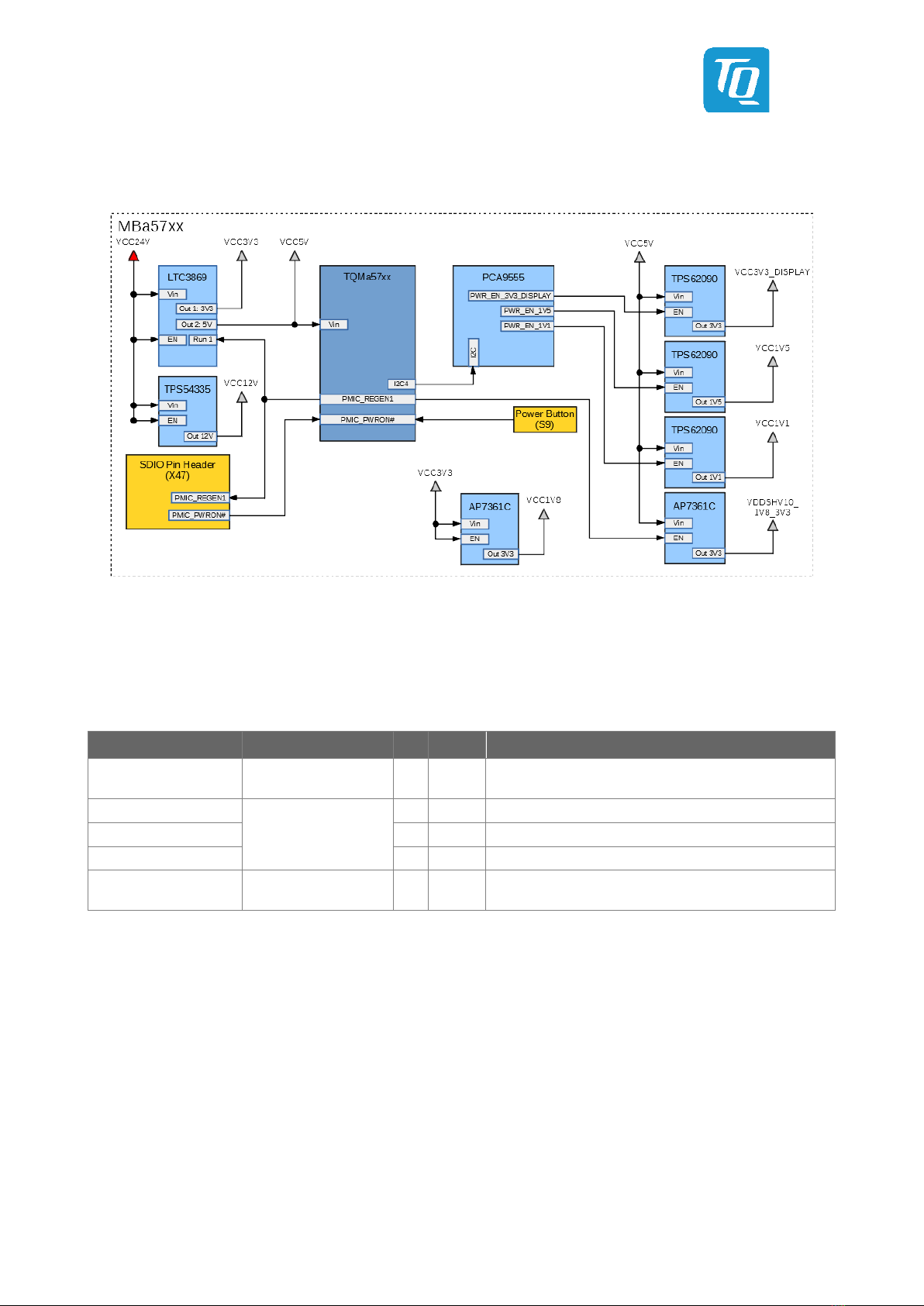
4.1.6 Power Management and Reset
Illustration 5: Block diagram Power
The following table shows the signals used for power management.
Table 12: Functions of power signals
Signal Source Dir. Default Remark
PMIC_REGEN1 TQMa57xx PMIC O Low Is activated by the TQMa57xx during power sequencing
and switches on the carrier board controller for 3.3 V.
PWR_EN_3V3_DISPLAY
Port-Expanders
PCA9555PW
O Low Enable for display power supply (X54)
PWR_EN_1V5 O Low Enable for 1.5 V supply
PWR_EN_1V1 O Low Enable for 1.1 V supply
PMIC_PWRON# Power Button /
SDIO extension header I High See TQMa57xx User's Manual. Can be used
with push button S9 and SDIO extension header.
Table of contents
Other TQ Motherboard manuals


