TQ TQMLS10 A Series User manual

TQMLS10xxA
User's Manual
TQMLS10xxA UM 0102
29.11.2019

User's Manual l TQMLS10xxA UM 0102 l © 2019, TQ-Systems GmbH Page i
TABLE OF CONTENTS
1. ABOUT THIS MANUAL................................................................................................................................................................................1
1.1 Copyright and license expenses.............................................................................................................................................................1
1.2 Registered trademarks...............................................................................................................................................................................1
1.3 Disclaimer......................................................................................................................................................................................................1
1.4 Imprint............................................................................................................................................................................................................1
1.5 Tips on safety................................................................................................................................................................................................2
1.6 Symbols and typographic conventions ...............................................................................................................................................2
1.7 Handling and ESD tips ...............................................................................................................................................................................2
1.8 Naming of signals........................................................................................................................................................................................3
1.9 Further applicable documents / presumed knowledge .................................................................................................................3
2. BRIEF DESCRIPTION ....................................................................................................................................................................................3
3. OVERVIEW......................................................................................................................................................................................................4
3.1 Block diagram...............................................................................................................................................................................................4
3.2 System components...................................................................................................................................................................................4
4. ELECTRONICS................................................................................................................................................................................................5
4.1 LS10xxA..........................................................................................................................................................................................................5
4.1.1 LS10xxA variants, block diagrams..........................................................................................................................................................5
4.1.2 LS10xxA variants, details...........................................................................................................................................................................6
4.2 Reset Configuration Word RCW..............................................................................................................................................................7
4.3 RCW source selection.................................................................................................................................................................................7
4.4 Clock supply..................................................................................................................................................................................................7
4.5 Power Modes................................................................................................................................................................................................7
4.6 JTAG.................................................................................................................................................................................................................8
4.7 Power supply................................................................................................................................................................................................9
4.7.1 Input voltage ................................................................................................................................................................................................9
4.7.2 Feedback voltages......................................................................................................................................................................................9
4.7.3 Power-up sequencing................................................................................................................................................................................9
4.7.4 Voltage monitoring....................................................................................................................................................................................9
4.7.5 Power consumption................................................................................................................................................................................ 10
4.8 Reset structure .......................................................................................................................................................................................... 11
4.9 Memory ....................................................................................................................................................................................................... 12
4.9.1 DDR4 SDRAM............................................................................................................................................................................................. 12
4.9.2 SPI NOR flash.............................................................................................................................................................................................. 12
4.9.3 EEPROM, 24LC256.................................................................................................................................................................................... 12
4.9.4 eMMC........................................................................................................................................................................................................... 12
4.10 Temperature sensor with EEPROM, SE97B....................................................................................................................................... 13
4.10.1 Temperature sensor, SE97B .................................................................................................................................................................. 13
4.10.2 EEPROM, SE97B......................................................................................................................................................................................... 13
4.11 RTC................................................................................................................................................................................................................ 14
4.12 UART............................................................................................................................................................................................................. 14
4.13 I2C bus.......................................................................................................................................................................................................... 15
4.14 TQMLS10xxA interfaces.......................................................................................................................................................................... 15
4.14.1 Pin multiplexing........................................................................................................................................................................................ 15
4.14.2 Pinout connectors X1, X2, X3, X4......................................................................................................................................................... 16
4.14.3 Assembly..................................................................................................................................................................................................... 20

User's Manual l TQMLS10xxA UM 0102 l © 2019, TQ-Systems GmbH Page ii
TABLE OF CONTENTS (continued)
5. MECHANICS................................................................................................................................................................................................ 21
5.1 Dimensions TQMLS1043A ..................................................................................................................................................................... 21
5.2 Dimensions TQMLS1046A / TQMLS1088A ....................................................................................................................................... 22
5.3 TQMLS10xxA connectors....................................................................................................................................................................... 23
5.4 Adaptation to the environment .......................................................................................................................................................... 24
5.5 Protection against external effects..................................................................................................................................................... 24
5.6 Thermal management............................................................................................................................................................................ 24
5.7 Structural requirements......................................................................................................................................................................... 24
5.8 Notes of treatment................................................................................................................................................................................... 24
6. SOFTWARE.................................................................................................................................................................................................. 24
7. SAFETY REQUIREMENTS AND PROTECTIVE REGULATIONS ......................................................................................................... 25
7.1 EMC............................................................................................................................................................................................................... 25
7.2 ESD................................................................................................................................................................................................................ 25
7.3 Operational safety and personal security......................................................................................................................................... 25
7.4 Climatic and operational conditions.................................................................................................................................................. 25
7.5 Reliability and service life....................................................................................................................................................................... 25
8. ENVIRONMENT PROTECTION................................................................................................................................................................ 26
8.1 RoHS............................................................................................................................................................................................................. 26
8.2 WEEE®.......................................................................................................................................................................................................... 26
8.3 REACH®........................................................................................................................................................................................................ 26
8.4 EuP................................................................................................................................................................................................................ 26
8.5 Battery.......................................................................................................................................................................................................... 26
8.6 Packaging ................................................................................................................................................................................................... 26
8.7 Other entries.............................................................................................................................................................................................. 26
9. APPENDIX ................................................................................................................................................................................................... 27
9.1 Acronyms and definitions...................................................................................................................................................................... 27
9.2 References.................................................................................................................................................................................................. 29

User's Manual l TQMLS10xxA UM 0102 l © 2019, TQ-Systems GmbH Page iii
TABLE DIRECTORY
Table 1: Terms and Conventions..............................................................................................................................................................2
Table 2: LS10xxA variants...........................................................................................................................................................................6
Table 3: RCW source selection..................................................................................................................................................................7
Table 4: TQMLS10xxA power consumption @ 5 V........................................................................................................................... 10
Table 5: RESET options............................................................................................................................................................................. 11
Table 6: SDHC_EXT_SEL options........................................................................................................................................................... 12
Table 7: I2C addresses............................................................................................................................................................................... 15
Table 8: Pinout connector X1................................................................................................................................................................. 16
Table 9: Pinout connector X2................................................................................................................................................................. 17
Table 10: Pinout connector X3................................................................................................................................................................. 18
Table 11: Pinout connector X4................................................................................................................................................................. 19
Table 12: Labels on TQMLS10xxA ........................................................................................................................................................... 20
Table 13: Connector assembled on TQMLS10xxA............................................................................................................................. 23
Table 14: Carrier board mating connectors ......................................................................................................................................... 23
Table 15: Climate and operational conditions.................................................................................................................................... 25
Table 16: Acronyms ..................................................................................................................................................................................... 27
Table 17: Further applicable documents.............................................................................................................................................. 29
ILLUSTRATION DIRECTORY
Illustration 1: Block diagram TQMLS10xxA (simplified) ..............................................................................................................................4
Illustration 2: Block diagram LS1043A..............................................................................................................................................................5
Illustration 3: Block diagram LS1046A..............................................................................................................................................................5
Illustration 4: Block diagram LS1088A..............................................................................................................................................................5
Illustration 5: Block diagram RCW source selection.....................................................................................................................................7
Illustration 6:Block diagram JTAG interface...................................................................................................................................................8
Illustration 7: Wiring of JTAG_TRST# and PORESET#....................................................................................................................................8
Illustration 8: Wiring of JTAG chain with CPU and CPLD ............................................................................................................................8
Illustration 9: Block diagram feedback voltages ...........................................................................................................................................9
Illustration 10: Block diagram Reset structure............................................................................................................................................... 11
Illustration 11: Block diagram 24LC256 EEPROM interface ....................................................................................................................... 12
Illustration 12: Block diagram SE97B temperature sensor......................................................................................................................... 13
Illustration 13: Memory Map SE97B EEPROM................................................................................................................................................ 13
Illustration 14: Block diagram RTC interface.................................................................................................................................................. 14
Illustration 15: Block diagram RTC buffering interface............................................................................................................................... 14
Illustration 16: Block diagram I2C bus 1 structure on TQMLS10xxA........................................................................................................ 15
Illustration 17: TQMLS10xxA assembly, top................................................................................................................................................... 20
Illustration 18: TQMLS10xxA assembly, bottom........................................................................................................................................... 20
Illustration 19: TQMLS1043A dimensions, side view................................................................................................................................... 21
Illustration 20: TQMLS1043A dimensions, top view.................................................................................................................................... 21
Illustration 21: TQMLS1043A dimensions, top view through TQMLS1043A....................................................................................... 21
Illustration 22: TQMLS1046A / TQMLS1088A dimensions, side view..................................................................................................... 22
Illustration 23: TQMLS1046A / TQMLS1088A dimensions, top view...................................................................................................... 22
Illustration 24: TQMLS1046A / TQMLS1088A dimensions, top view through TQMLS1046A / TQMLS1088A........................... 22

User's Manual l TQMLS10xxA UM 0102 l © 2019, TQ-Systems GmbH Page iv
REVISION HISTORY
Rev. Date Name Pos. Modification
0100 12.08.2019 Petz First issue
0101 07.10.2019 Petz
All
1.9
Table 2
Table 4
4.7.2
4.9.1
4.12
10, 21
7.5
(5)
Hyperlinks updated, Links to TQMLS10xxA-specific BSPs added
Link to PTXdist documentation removed, Link to Yocto documentation added
Clarified and corrected
Values added
Reworked, Illustration 9 added
Information added
Chapter added
Footnotes added
Updated
Link to LS1043A Errata added
0102 29.11.2019 Petz
All
Table 5
4.14.2
Links updated
Clarified
Chapters 4.14.2 to 4.14.5 merged

User's Manual l TQMLS10xxA UM 0102 l © 2019, TQ-Systems GmbH Page 1
1. ABOUT THIS MANUAL
1.1 Copyright and license expenses
Copyright protected © 2019 by TQ-Systems GmbH.
This User's Manual may not be copied, reproduced, translated, changed or distributed, completely or partially in electronic,
machine readable, or in any other form without the written consent of TQ-Systems GmbH.
The drivers and utilities for the components used as well as the BIOS are subject to the copyrights of the respective
manufacturers. The licence conditions of the respective manufacturer are to be adhered to.
Bootloader-licence expenses are paid by TQ-Systems GmbH and are included in the price.
Licence expenses for the operating system and applications are not taken into consideration and must be calculated / declared
separately.
1.2 Registered trademarks
TQ-Systems GmbH aims to adhere to copyrights of all graphics and texts used in all publications, and strives to use original
or license-free graphics and texts.
All brand names and trademarks mentioned in this User's Manual, including those protected by a third party, unless specified
otherwise in writing, are subjected to the specifications of the current copyright laws and the proprietary laws of the present
registered proprietor without any limitation. One should conclude that brand and trademarks are rightly protected by a third
party.
1.3 Disclaimer
TQ-Systems GmbH does not guarantee that the information in this User's Manual is up-to-date, correct, complete or of good
quality. Nor does TQ-Systems GmbH assume guarantee for further usage of the information. Liability claims against TQ-Systems
GmbH, referring to material or non-material related damages caused, due to usage or non-usage of the information given in this
User's Manual, or due to usage of erroneous or incomplete information, are exempted, as long as there is no proven intentional
or negligent fault of TQ-Systems GmbH.
TQ-Systems GmbH explicitly reserves the rights to change or add to the contents of this User's Manual or parts of it without
special notification.
Important Notice:
Before using the Starterkit MBLS10xxA or parts of the schematics of the MBLS10xxA, you must evaluate it and determine if it is
suitable for your intended application. You assume all risks and liability associated with such use. TQ-Systems GmbH makes no
other warranties including, but not limited to, any implied warranty of merchantability or fitness for a particular purpose. Except
where prohibited by law, TQ-Systems GmbH will not be liable for any indirect, special, incidental or consequential loss or damage
arising from the usage of the Starterkit MBLS10xxA or schematics used, regardless of the legal theory asserted.
1.4 Imprint
TQ-Systems GmbH
Gut Delling, Mühlstraße 2
D-82229 Seefeld
Tel: +49 8153 9308–0
Fax: +49 8153 9308–4223
E-Mail: Info@TQ-Group
Web: TQ-Group

User's Manual l TQMLS10xxA UM 0102 l © 2019, TQ-Systems GmbH Page 2
1.5 Tips on safety
Improper or incorrect handling of the product can substantially reduce its life span.
1.6 Symbols and typographic conventions
Table 1: Terms and Conventions
Symbol Meaning
This symbol represents the handling of electrostatic-sensitive modules and / or components. These
components are often damaged / destroyed by the transmission of a voltage higher than about 50 V.
A human body usually only experiences electrostatic discharges above approximately 3,000 V.
This symbol indicates the possible use of voltages higher than 24 V.
Please note the relevant statutory regulations in this regard.
Non-compliance with these regulations can lead to serious damage to your health and also cause
damage / destruction of the component.
This symbol indicates a possible source of danger. Acting against the procedure described can lead to
possible damage to your health and / or cause damage / destruction of the material used.
This symbol represents important details or aspects for working with TQ-products.
Command
A font with fixed-width is used to denote commands, contents, file names, or menu items.
1.7 Handling and ESD tips
General handling of your TQ-products
The TQ-product may only be used and serviced by certified personnel who have taken note of the
information, the safety regulations in this document and all related rules and regulations.
A general rule is: do not touch the TQ-product during operation. This is especially important when
switching on, changing jumper settings or connecting other devices without ensuring beforehand
that the power supply of the system has been switched off.
Violation of this guideline may result in damage / destruction of the TQMLS10xxA and be dangerous
to your health.
Improper handling of your TQ-product would render the guarantee invalid.
Proper ESD handling
The electronic components of your TQ-product are sensitive to electrostatic discharge (ESD).
Always wear antistatic clothing, use ESD-safe tools, packing materials etc., and operate your TQ-
product in an ESD-safe environment. Especially when you switch modules on, change jumper settings,
or connect other devices.

User's Manual l TQMLS10xxA UM 0102 l © 2019, TQ-Systems GmbH Page 3
1.8 Naming of signals
A hash mark (#) at the end of the signal name indicates a low-active signal.
Example: RESET#
If a signal can switch between two functions and if this is noted in the name of the signal, the low-active function is marked with
a hash mark and shown at the end.
Example: C / D#
If a signal has multiple functions, the individual functions are separated by slashes when they are important for the wiring.
The identification of the individual functions follows the above conventions.
Example: WE2# / OE#
1.9 Further applicable documents / presumed knowledge
•Specifications and manual of the modules used:
These documents describe the service, functionality and special characteristics of the module used (incl. BIOS).
•Specifications of the components used:
The manufacturer's specifications of the components used, for example CompactFlash cards, are to be taken note of.
They contain, if applicable, additional information that must be taken note of for safe and reliable operation.
These documents are stored at TQ-Systems GmbH.
•Chip errata:
It is the user's responsibility to make sure all errata published by the manufacturer of each component are taken note of.
The manufacturer’s advice should be followed.
•Software behaviour:
No warranty can be given, nor responsibility taken for any unexpected software behaviour due to deficient components.
•General expertise:
Expertise in electrical engineering / computer engineering is required for the installation and the use of the device.
The following documents are required to fully comprehend the following contents:
•MBLS10xxA circuit diagram
•MBLS10xxA User's Manual
•LS10xxA Data Sheets
•LS10xxA Reference Manuals
•U-Boot documentation: www.denx.de/wiki/U-Boot/Documentation
•Yocto documentation: www.yoctoproject.org/docs/
•TQ-Support Wiki TQMLS1043A / TQMLS1023A: TQ-Wiki TQMLS1043A
•TQ-Support Wiki TQMLS1046A / TQMLS1026A: TQ-Wiki TQMLS1046A
•TQ-Support Wiki TQMLS1088A: TQ-Wiki TQMLS1088A
2. BRIEF DESCRIPTION
This User's Manual describes the hardware of the TQMLS10xxA, Rev. 02xx and refers to some software settings. A certain
TQMLS10xxA derivative does not necessarily provide all features described in this User's Manual. This User's Manual does also
not replace the NXP CPU Reference Manuals. The information provided in this User's Manual is only valid in connection with the
tailored boot loader, which is preinstalled on the TQMLS10xxA, and the BSP provided by TQ-Systems GmbH. See also chapter 6.
The TQMLS10xxA is a universal Minimodule based on the NXP Layerscape CPUs LS1043A / LS1046A / LS1088A. The Layerscape
CPU is a Dual Cortex®A7 with QorIQ technology. The TQMLS10xxA extends the TQ-Systems GmbH product range and offers an
outstanding computing performance. A suitable CPU derivative (LS1043A / LS1046A / LS1088A) can be selected for each
requirement. All essential CPU pins are routed to the TQMLS10xxA connectors. There are therefore no restrictions for customers
using the TQMLS10xxA with respect to an integrated customised design. Furthermore all components required for the CPU to
function like DDR4 SDRAM, eMMC, power supply and power management are integrated on the TQMLS10xxA.
The main TQMLS10xxA characteristics are:
•CPU derivatives LS1043A (LS1023A), LS1046A (LS1026A), LS1088A
•DDR4 SDRAM with ECC
•eMMC and QSPI NOR flash
•Single supply voltage 5 V
•On-board RTC / EEPROM / temperature sensor
The MBLS10xxA also serves as carrier board and reference platform for the TQMLS10xxA.

User's Manual l TQMLS10xxA UM 0102 l © 2019, TQ-Systems GmbH Page 4
3. OVERVIEW
3.1 Block diagram
TQMLS10xxA connector
IO
Muxing
IO
Muxing
QSPI NOR Flash
QSPI NOR Flash
eMMC Flash
Layerscape CPU
LS1043A (LS1023A)
LS1046A (LS1026A)
LS1088A
DDR4
DDR4
DDR4
DDR4
DDR4 (ECC)
Voltage
Monitoring
Temp. Sensor
RTC
EEPROM
Power
Supply
Board Controller
(Housekeeping)
CPLD
TQMLS10xxA connector
TQMLS10xxA connector
TQMLS10xxA connector
Illustration 1: Block diagram TQMLS10xxA (simplified)
3.2 System components
The TQMLS10xxA provides the following key functions and characteristics:
•Layerscape CPUs LS1043A (LS1023A), LS1046A (LS1026A), LS1088A
•Oscillators
•Reset structure
•Power supply and power-sequencing
•Voltage supervision
•Housekeeping µController
•Temperature sensor
•RTC
•EEPROM
•DDR4 SDRAM with ECC
•QSPI NOR flash
•eMMC
•Four connectors (420 pins)
All essential CPU pins are routed to the TQMLS10xxA connectors. There are therefore no restrictions for customers using the
TQMLS10xxA with respect to an integrated customised design.
All TQMLS10xxA versions are fully pin-compatible and therefore interchangeable. The functionality of the different TQMLS10xxA
is mainly determined by the features provided by the respective CPU.


User's Manual l TQMLS10xxA UM 0102 l © 2019, TQ-Systems GmbH Page 6
4.1.2 LS10xxA variants, details
The following table shows the features provided by the different variants.
Fields with a red background indicate differences; fields with a green background indicate compatibility.
Table 2: LS10xxA variants
Feature LS1043A LS1046A LS1088A
Cores
Number of cores 4 × A53 Cortex®v8 4 × A72 Cortex®v8 8 × A53 Cortex®v8
Bus width 64-bit 64-bit 64-bit
Max. frequency (MHz) 1600 1600 1600
Memory Size
L1 cache 32 kB I/D 32 kB D cache/ 48 kB I Cache 32 kB I/D
L2 cache Shared 1 MB Shared 2 MB Shared 2 × 1 MB
Main memory type 1 × DDR3L/4, 1600 MT/s 1 × DDR4, 2100 MT/s 1 × DDR4, 2100 MT/s
Max. memory size 1 TB (40-bit address) 1 TB (40-bit address) 1 TB (40-bit address)
Interconnect
CCI 400 400 MHz 600 MHz 700 MHz
I/O
Ethernet controllers
1 × 10 Gbit/s XFI;
1 × QSGMII;
4 × 1 Gbit/s SGMII;
2 × 2.5 Gbit/s SGMII
2 × RGMII
2 × 10 Gbit/s XFI;
1 × QSGMII;
5 × 1 Gbit/s SGMII;
3 × 2.5 Gbit/s SGMII
2 × RGMII
2 × 10 Gbit/s XFI;
2 × QSGMII;
4 × 1 Gbit/s SGMII;
2 × 2.5 Gbit/s SGMII
2 × RGMII
SerDes lanes 4 lanes at up to 10 GHz 8 lanes at up to 10 GHz 8 lanes at up to 10 GHz
PCI Express controllers
3 × Gen 2.0 controllers; 5 Gbit/s
Root complex supported,
×4, ×2, and ×1 link widths
3 × Gen 3.0 controllers; 8 Gbit/s
Root complex or end point supported,
×4, ×2, and ×1 link widths
3 × Gen 3.0 controllers; 8 Gbit/s
Root complex or end point supported,
×4, ×2, and ×1 link widths
SATA 1 × SATA controller
up to 6.0 Gbit/s
1 × SATA controller
up to 6.0 Gbit/s
1 × SATA controller
up to 6.0 Gbit/s
USB 3 × USB 3.0 controllers; 5 Gbit/s 3 × USB 3.0 controllers; 5 Gbit/s 2 × USB 3.0 controllers; 5 Gbit/s
QE HDLC, Transparent UART, TDM/SI Not supported HDLC, Transparent UART, TDM/SI
Integrated Flash Controller
(IFC)
8-/16-bit data width,
28-bit address width
8-/16-bit data width,
28-bit address width
8-/16-bit data width,
28-bit address width
Other peripherals
1 × eSDHC; 1 × QSPI; 1 × SPI;
4 × I2C; 2 × DUART; 6 × LPUART;
8 × FlexTimer
1 × eSDHC; 1 × QSPI; 1 × SPI;
4 × I2C; 2 × DUART; 6 × LPUART;
8 × FlexTimer
1 × eSDHC; 1 × QSPI; 1 × SPI;
4 × I2C; 2 × DUART;
4 × FlexTimer
Clocking
Single source clocking DIFF_SYSCLK/
DIFF_SYSCLK_B with LVDS receiver
DIFF_SYSCLK/
DIFF_SYSCLK_B with LVDS receiver
DIFF_SYSCLK/
DIFF_SYSCLK_B with HCSL receiver
Package
Package 23 mm × 23 mm, 0.8 mm pitch,
780-pin FC-PBGA Unlidded
23 mm × 23 mm, 0.8 mm pitch,
780-pin FC-PBGA Unlidded
23 mm × 23 mm, 0.8 mm pitch,
780-pin FC-PBGA Lidded

User's Manual l TQMLS10xxA UM 0102 l © 2019, TQ-Systems GmbH Page 7
4.2 Reset Configuration Word RCW
The Reset Configuration Word RCW can be taken from the LS1043A / LS1046A / LS1088A Reference Manuals (1).
4.3 RCW source selection
On the TQMLS10xxA the RCW source selection is controlled by a CPLD. An external pin strapping is not required.
BOOT_
SRC[0:1]
Pin-Strapping
- Active driver during RESET#
- High-Z during normal operation
IFC
BUS
PORESET#
Board
Controller
RESIN#
LS CPU
CPLD
TQMLS10xxA
connectors
Illustration 5: Block diagram RCW source selection
The boot source is selected with signals BOOT_CFG[1:0].
Table 3: RCW source selection
BOOT_CFG1 BOOT_CFG0 RCW Source
Low Low QSPI NOR Flash
Low High I2C (LS1088 only)
High Low SDHC
High High eMMC (LS1088 only)
BOOT_CFG[1:0] is initialized with a Pull-Up to 3.3V on the TQMLS10xxA.
After the TQMLS10xxA is powered-up, the CPLD applies the pin strapping.
4.4 Clock supply
The clock supply on the TQMLS10xxA corresponds to the structure „Multiple Reference clocking“, described in (1).
•SYSCLK = 100 MHz
•DDRCLK = 100 MHz (LS1043A, LS1046A), 133.33 MHz (LS1088A)
•ECx_GTX_CLK125 is not generated on the TQMLS10xxA, has to be generated externally.
•Differential SERDES clocks are not generated on the TQMLS10xxA, have to be generated externally.
4.5 Power Modes
Currently no power modes are implemented.

User's Manual l TQMLS10xxA UM 0102 l © 2019, TQ-Systems GmbH Page 8
4.6 JTAG
The JTAG interface is routed to the connectors. Signals TMS, and TRST# have 10 kΩ Pull-Ups to 1.8 V on the TQMLS10xxA.
Illustration 6: Block diagram JTAG interface
Signal TRST_CPU# is connected with PORESET# by resistors. TRST# is pulled at the same time as PORESET#, but can also be pulled
Low using an external debugger, while PORESET# remains unchanged.
Illustration 7: Wiring of JTAG_TRST# and PORESET#
The CPLD is also in the JTAG chain of the CPU.
CPLD CPU
Board
Controller
TRST#
TDI
TDO
TDI TDO TDI TDO
TMS
TCK
TQMLS10xxA
connectors
Illustration 8: Wiring of JTAG chain with CPU and CPLD
The JTAG access to the CPU is activated by default.
The Board Controller can be used to switch to the JTAG port of the CPLD.
User's Manual l TQMLS10xxA UM 0102 l © 2019, TQ-Systems GmbH Page 9
4.7 Power supply
4.7.1 Input voltage
The TQMLS10xxA requires a 5 V supply with a maximum tolerance of ±5 %.
4.7.2 Feedback voltages
The voltages DVDD, LVDD, TVDD, and VCCGPIIN can be fed back according to customer requirements:
Power
V
IN
1.2 V
TQMLS10xxA connectors
Power 3.3 V
Power 2.5 V
Power 1.8 V
TVDD
1.2V / 1.8V / 2.5V
DVDD
1.8V / 3.3V
LVDD
1.8V / 2.5V
VCCGPIIN
1.8V / 2.5V / 3.3V
Carrier BoardTQMLS10xxA
Illustration 9: Block diagram feedback voltages
The TQMLS10xxA provides the respective voltages in order to enable a simple connection according to customer requirements
on the carrier board. The voltages generated on the TQMLS10xxA may only be used for the TQMLS10xxA itself. Further loads by
external circuitry on a carrier board are not permitted and may lead to supply and monitoring errors.
Voltage EVDD is switched on the TQMLS10xxA:
•EVDD = 3.3V if SDHC_EXT_SEL = 1 (SD card)
•EVDD = 1.8V if SDHC_EXT_SEL = 0 (eMMC)
4.7.3 Power-up sequencing
The power-up sequencing is executed and monitored by the TQMLS10xxA.PORESET# is kept Low during power-up.
4.7.4 Voltage monitoring
All voltages generated on the TQMLS10xxA are monitored.

User's Manual l TQMLS10xxA UM 0102 l © 2019, TQ-Systems GmbH Page 10
4.7.5 Power consumption
The given power consumptions have to be seen as typical values. The power consumption of the TQMLS10xxA strongly depends
on the application, the mode of operation, the environmental temperature, and the operating system.
The power supply of the carrier board should be designed for an output power of 18 to 20 watts.
The following table shows typical power consumption of the TQMLS10xxA under various operating conditions.
Table 4: TQMLS10xxA power consumption @ 5 V
Mode of operation TQMLS1043A TQMLS1046A TQMLS1088A T environment
U-Boot, idle 4.08 W 7 W 8.64 W
+25 °C
U-Boot, memory test 4.24 W 8.4 W 9.44 W
Linux, idle 3.92 W 7.1 W 8 W
Linux, 100 % CPU load 6 W (1) 11.9 W (2) 12.32 W (3)
U-Boot, idle 5.76 W 11.6 W 12.76 W
+85 °C
U-Boot, memory test 6.72 W 14.2 W 15.72 W
Linux, 100 % CPU load 8.05 W (1) 15.6 W (2) 18.9 W (3)
Attention: Destruction or malfunction, TQMLS10xxA heat dissipation
The TQMLS10xxA belongs to a performance category in which a cooling system is essential.
It is the user’s sole responsibility to define a suitable heat sink (weight and mounting position)
depending on the specific mode of operation (e.g., dependence on clock frequency, stack height,
airflow, and software). Particularly the tolerance chain (PCB thickness, board warpage, BGA balls, BGA
package, thermal pad, heatsink) as well as the maximum pressure on the LS10xxA must be taken into
consideration when connecting the heat sink, see (2).
The LS10xxA is not necessarily the highest component. Inadequate cooling connections can lead to
overheating of the TQMLS10xxA and thus malfunction, deterioration or destruction.
1: stressapptest -s 3600 -M 700 -m 4 -C 4 -i 4
2: stressapptest -s 3600 -M 1024 -m 4 -C 4 -i 4
3: stressapptest -s 3600 -M 512 -m 4 -C 4 -i 4

User's Manual l TQMLS10xxA UM 0102 l © 2019, TQ-Systems GmbH Page 11
4.8 Reset structure
If RESIN# is disabled, the Board Controller starts the initialization of the TQMLS10xxA.
If no errors occur during initialization and when power supplies are OK, the CPU is started via PORESET#.
RESET# is provided at the TQMLS10xxA connector via signal RESET_OUT#.
PORESET# should not be connected at the TQMLS10xxA connector.
A red LED (V26) signals the RESET# state.
HRESET# of the CPU is directly available at the TQMLS10xxA connector (4.7 kΩ Pull-Up to 1.8 V).
CPU signal RESET_REQ# is processed by the Board Controller and routed to the TQMLS10xxA connectors.
CPLD
Reset
Monitor
RESIN#
LS10xxA
PORESET#
PORESET#
Board
Controller
RESET_OUT#
V26
CPLD
Voltage Monitoring
PGOOD
SYSC_POR#
RESET_REQ#
Open
Drain
RESET_REQ_OUT#
JTAG_TRST#
DDR4
DDR4_RST_EN
TQMLS10xxA
connectors
Illustration 10: Block diagram Reset structure
•RESIN# keeps the TQMLS10xxA in RESET#
•Further RESET# sources are:
oBy software via Board Controller
oBy software via CPU RESET_REQ
oVIN Power Fail
Table 5: RESET options
Wiring at RESIN# Reset function
Open Drain Self-reset possible
Logic Low at RESIN# triggers RESET
Open, or Pull-Up ≥47 kΩto VCC3V3 Self-reset possible
RESET_REQ_OUT# can trigger RESIN# on TQMLS10xxA
Pull-Up <10 kΩto VCC3V3
No
self-reset possible
RESET_REQ_OUT# cannot trigger RESIN# on TQMLS10xxA
Push/Pull driver
No
self-reset, but external RESET possible
Logic High at RESIN# overrides RESET_REQ_OUT# on TQMLS10xxA

User's Manual l TQMLS10xxA UM 0102 l © 2019, TQ-Systems GmbH Page 12
4.9 Memory
4.9.1 DDR4 SDRAM
Depending on the CPU derivative, the TQMLS10xxA supports up to 8 Gbyte DDR4 SDRAM.
ECC is optionally available and is assembled as an additional DDR4 SDRAM component.
4.9.2 SPI NOR flash
Up to two QSPI NOR flash devices can be assembled on the TQMLS10xxA.
4.9.3 EEPROM, 24LC256
A 24LC256 series EEPROM with 256 Kbit (32 kB × 8 bit) is assembled on the TQMLS10xxA.
Write Protection can be controlled by
•CPLD
•Board Controller
•USRGPIO pin
A 4.7 kΩ Pull-Down is assembled on the TQMLS10xxA, thus write access is permitted.
Write protection is controlled by the CPLD. Write_Protect# of the EEPROM is not connected directly to the TQMLS10xxA
connectors, but can be controlled indirectly via USR_GPIO_1.
EEPROM
Write_Protect#
I²C bus
LS10xxA
Board
Controller
CPLD
USRGPIO_1
TQMLS10xxA
connector
Illustration 11: Block diagram 24LC256 EEPROM interface
4.9.4 eMMC
The LS10xxA derivatives provide only one SDHC controller. Therefore the SD card interface cannot be used when an eMMC is
assembled on the TQMLS10xxA. Hence the SDHC interface is routed to the TQMLS10xxA connectors and can be enabled with
the SDHC_EXT_SEL control signal. A Pull-Down on the TQMLS10xxA activates the eMMC on the TQMLS10xxA by default.
Table 6: SDHC_EXT_SEL options
SDHC_EXT_SEL Configuration
High External SDHC
Low On-board eMMC

User's Manual l TQMLS10xxA UM 0102 l © 2019, TQ-Systems GmbH Page 13
4.10 Temperature sensor with EEPROM, SE97B
4.10.1 Temperature sensor, SE97B
A temperature sensor SE97B is assembled on the TQMLS10xxA, which measures the environmental temperature.
Illustration 12: Block diagram SE97B temperature sensor
The temperature sensor has I2C address 0x18 / 001 1000b
The accuracy of the temperature sensor is as follows:
•Max. ±1 °C between +75 °C and +95 °C
•Max. ±2 °C between +40 °C and +125 °C
•Max. ±3 °C between –40 °C and +125 °C
Signal TEMP_CRIT_MOD# of the temperatures sensor is routed to the TQMLS10xxA connector. It provides a warning at a
programmed trigger level. During power-up the sensor is configured to T_CRIT_LOKAL = +95 °C by the Board Controller.
This value can be overwritten by the boot loader, the operating system, or the application.
The signal has an Open Drain output, a Pull-Up to 3.3 V is provided on the TQMLS10xxA.
4.10.2 EEPROM, SE97B
The SE97B also contains a 2 Kbit (256 × 8 Bit) EEPROM. The EEPROM is divided into two parts.
The lower 128 bytes (00h to 7Fh) can be Permanent Write Protected (PWP) or Reversible Write Protected (RWP) by software.
The upper 128 bytes (80h to FFh) are not write protected and can be used for general purpose data storage.
Illustration 13: Memory Map SE97B EEPROM
The EEPROM can be accessed with the following two I2C addresses.
•EEPROM (Normal Mode): 0x50 / 101 0000b
•EEPROM (Protected Mode): 0x30 / 011 0000b

User's Manual l TQMLS10xxA UM 0102 l © 2019, TQ-Systems GmbH Page 14
4.11 RTC
An RTC type PCF85063A is assembled. RTC signal CLKOUT (32 kHz) is routed to the TQMLS10xxA connector (X2-118).
RTC signal INT# can be used in several ways:
•External use: Signal is accessible at the TQMLS10xxA connector, Pull-Up to 3.3 V on the TQMLS10xxA.
•The signal is also available on the Board Controller for wake-up.
TQMLS10xxA connector
3.3 V
LDO
5.0 V
VBAT
CLKOUT
Board
Controller
LS CPU
RTC
I²C Bus
32 kHz
Level
Shifter
3.3 V → 1.8 V
RTC_INT
_OUT#
CPU_RTC
CLKOUT
INT#
Illustration 14: Block diagram RTC interface
The RTC has I2C address 0x51 / 101 0001b
The RTC is clocked with a 32.768 kHz crystal with an accuracy of ±20 ppm at +25 °C. This equals to a maximum deviation
of 1.7 seconds per day. The accuracy at +85 °C is ±30 ppm. This equals to a maximum deviation of 2.6 seconds per day.
The RTC is supplied by VBAT. A GoldCap®or a battery is required.
Illustration 15: Block diagram RTC buffering interface
4.12 UART
It is recommended to assemble 4.7 kΩ Pull-Ups at the UART_SOUT signals on the carrier board.
For details contact TQ-Support.

User's Manual l TQMLS10xxA UM 0102 l © 2019, TQ-Systems GmbH Page 15
4.13 I2C bus
The I2C devices on the TQMLS10xxA are connected to the I2C1 bus.
LS10xxA
RTC
CPLD
EEPROM
Board
Controller
Temp. Sensor
+
EEPROM
IIC1
Optional
external
Pull-Ups
required
External
Devices
DVDD ↔ 3.3 V (LDO)
Level Shifter
3.3 V (LDO) ↔ VCC3V3
IIC1_MOD
I2C_BRD
L-ASC10
Level Shifter
24LC256T PCF95063 SE97BTP
Temp. Sensor
+
EEPROM
SE97BTP
I2C3_MCU
IIC1
Illustration 16: Block diagram I2C bus 1 structure on TQMLS10xxA
4.7 kΩPull-Ups at the I2C bus are assembled on the TQMLS10xxA. More devices can be connected to the bus but then additional
external Pull-Ups may be required on account of the higher capacitive load.
Table 7: I2C addresses
Device Function 7-bit address Remark
Connected to Board Controller, not accessible
L-ASC10 Voltage Monitoring
0x60 / 110 0000b
–
MachX03 CPLD (n.a.) –
SE97B
Temperature sensor
0x1B / 001 1011b
Access to temperature registers
EEPROM
0x53 / 101 0011b
R/W access in Normal Mode
EEPROM
0x33 / 011 0011b
R/W access in Protected Mode
Connected to LS10xxA, accessible
24LC256 EEPROM
0x57 / 101 0111b
–
STM32 Board Controller
0x11 / 001 0001b
Should not be altered
PCF85063A RTC
0x51 / 101 0001b
–
SE97B
Temperature sensor
0x18 / 001 1000b
Access to temperature registers
EEPROM
0x50 / 101 0000b
R/W access in Normal Mode
EEPROM
0x30 / 011 0000b
R/W access in Protected Mode
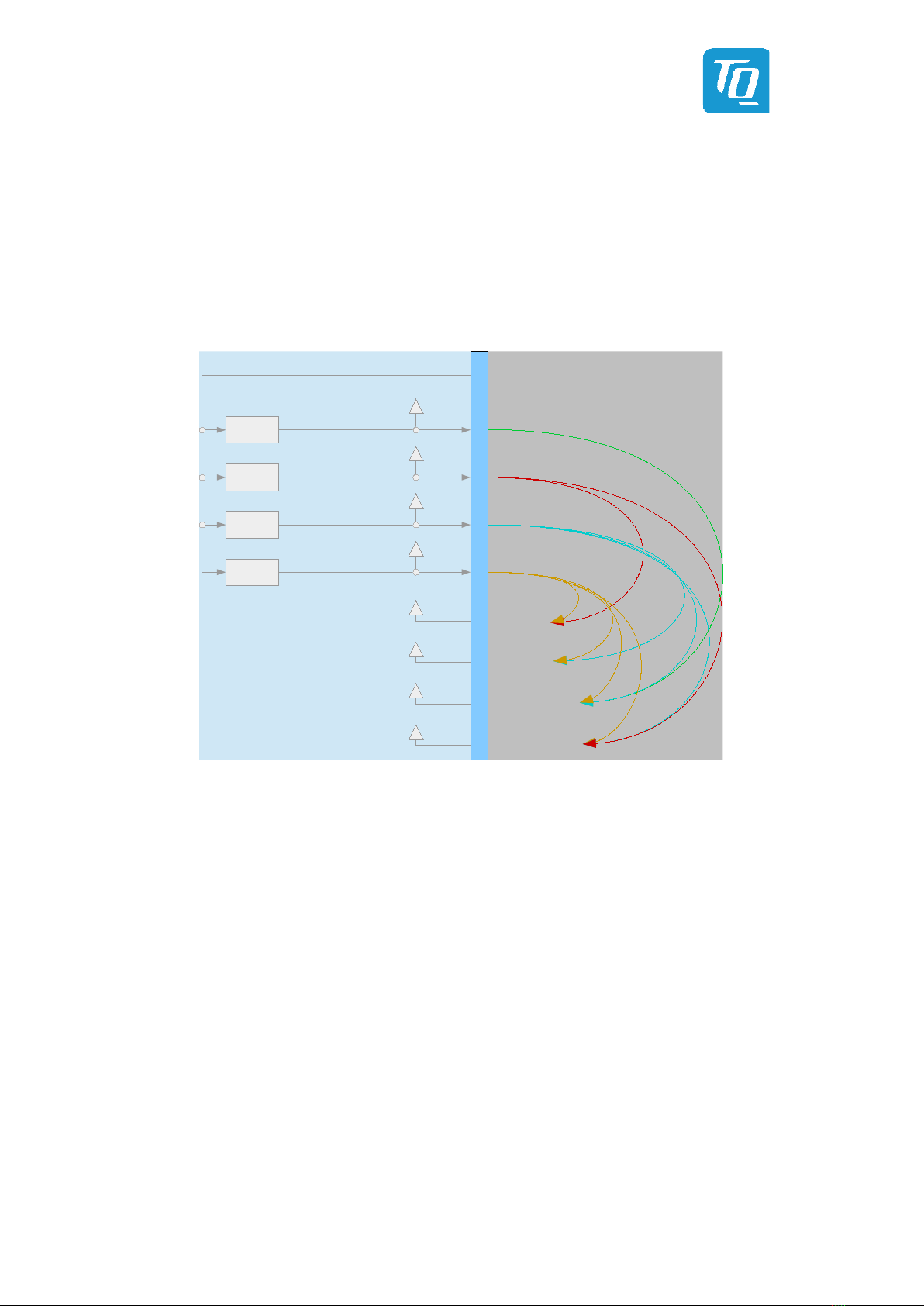
4.14 TQMLS10xxA interfaces
4.14.1 Pin multiplexing
When using the processor signals the multiple pin configurations by different processor-internal function units must be taken
note of. The pin assignment listed in Table 8 to Table 11 refer to the corresponding standard BSPs of TQ-Systems GmbH
in combination with the Starterkit MBLS10xxA. For standard BSPs, see 1.9.
Attention: Destruction or malfunction
Depending on the configuration many CPU pins can provide several different functions.
Please take note of the information concerning the configuration of these pins in (1), before
integration or start-up of your carrier board / Starterkit.
This manual suits for next models
3
Table of contents
Other TQ Motherboard manuals


 manual ")


