unicore UT986eb User manual

UT986eb User Manual
i
Revision History
Version
Revision History
Date
R1.0
First release
Nov., 2023

ii
Legal right notice
This manual provides information and details on the products of Unicore Communication, Inc.
(“Unicore”) referred to herein.
All rights, title and interest to this document and the information such as data, designs, layouts
contained in this manual are fully reserved, including but not limited to the copyrights, patents,
trademarks and other proprietary rights as relevant governing laws may grant, and such rights
may evolve and be approved, registered or granted from the whole information aforesaid or any
part(s) of it or any combination of those parts.
Unicore holds the trademarks of “和芯星通”, “UNICORECOMM” and other trade name, trademark,
icon, logo, brand name and/or service mark of Unicore products or their product serial referred
to in this manual (collectively “Unicore Trademarks”).
This manual or any part of it, shall not be deemed as, either expressly, implied, by estoppel or
any other form, the granting or transferring of Unicore rights and/or interests (including but not
limited to the aforementioned trademark rights), in whole or in part.
Disclaimer
The information contained in this manual is provided “as is” and is believed to be true and
correct at the time of its publication or revision. This manual does not represent, and in any
case, shall not be construed as a commitments or warranty on the part of Unicore with respect
to the fitness for a particular purpose/use, the accuracy, reliability and correctness of the
information contained herein.
Information, such as product specifications, descriptions, features and user guide in this
manual, are subject to change by Unicore at any time without prior notice, which may not be
completely consistent with such information of the specific product you purchase.
Should you purchase our product and encounter any inconsistency, please contact us or our
local authorized distributor for the most up-to-date version of this manual along with any
addenda or corrigenda.

UT986eb User Manual
iii
Foreword
This manual provides information on the hardware composition and design of the UT986
evaluation board (UT986eb).
Target Readers
This document is written for technicians who are familiar with GNSS receivers.

I
Contents
1Product Overview ...................................................................................1
2Interfaces ...............................................................................................4
3Power Supply .........................................................................................6
3.1 3.3 V LDO Power Supply..................................................................................................7
3.2 5 V DC/DC Power Supply ................................................................................................8
3.3 Backup Power Supply......................................................................................................9
4Antenna Circuit.....................................................................................11
4.1 Antenna Short Protection Circuit................................................................................. 11
4.2 Antenna Feed Circuit .................................................................................................... 12
5LED Indicators ......................................................................................13
6UT986 Series Peripheral Design............................................................14
7Debug Support .....................................................................................17
Appendix ....................................................................................................18

UT986eb User Manual
UC-08-M37 EN R1.0 Product Overview 1
1Product Overview
UT986eb is the evaluation board (EB) of UT986. It consists of the module UT986, a 3.3V
low dropout regulator (LDO), a 5V DC/DC boost circuit, an antenna short protection
circuit and peripheral interfaces.
The schematics of the evaluation board can be used as the reference design for the
module UT986.
UT986eb
UT986
ANT_IN
VBCKP
PPS
COM1
COM2
RSTN
BAT
Dual-row pins
Dual-row pins
VCC 5V DC/DC
Antenna
protection
circuit
5V
LDO 3V3
Figure 1-1 UT986eb Block Diagram

2 Product Overview UC-08-M37 EN R1.0
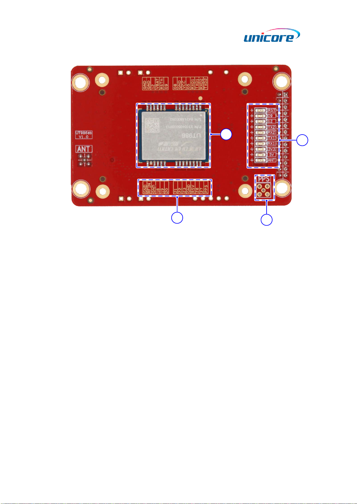
The appearance of UT986eb is as follows:
2
3
4
1
Figure 1-2 Top View of UT986eb
(1) Silkscreen: It marks the signals of the pins. The smaller holes around are used
to mount the UT986 socket. The printing adopts exposed copper to ensure the
flatness of the surface.
(2) UT986 module: The pin pads are designed long, which is convenient for
soldering, testing and debugging. For detailed packaging information, refer to
the PCB document.
(3) PPS connector: To measure the PPS signal, solder an MMCX connector here.
(4) LED indicators: Indicating the status of the power supply, reset, antenna short
circuit, and UART.

UT986eb User Manual
UC-08-M37 EN R1.0 Product Overview 3
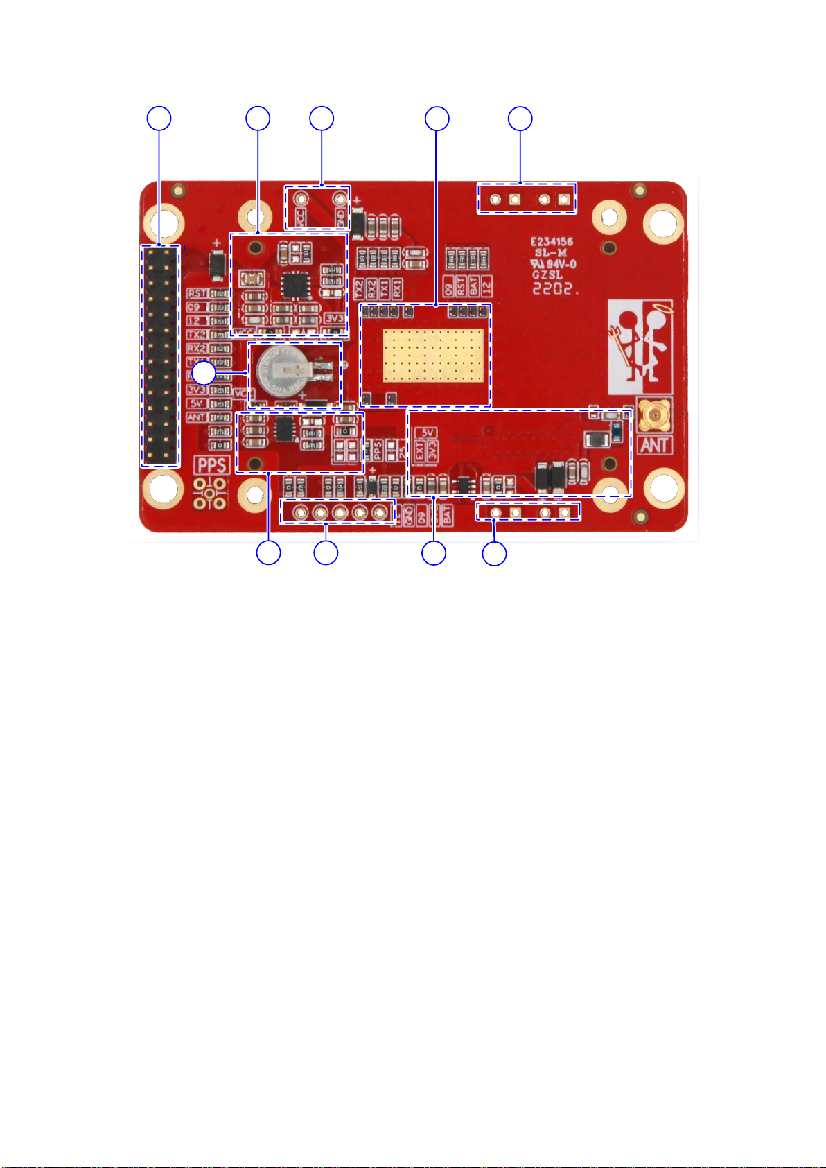
12
4
5
6
7 3 8 1
3
Figure 1-3 Bottom View of UT986eb
(1) Ports used to connect jumpers
(2) Anti-static design and heat dissipation with
exposed copper
(3) Debug ports
(4) VCC power supply and LDO circuit
(5) Dual-row pins as external interfaces
(6) Backup battery
(7) 5 V DC/DC boost circuit for antenna feeding
(8) Antenna feed circuit

4 Interfaces UC-08-M37 EN R1.0
2Interfaces
The dual-row 28 pins serve as the external interfaces of the evaluation board and the
pin pitch is 2 mm. The interfaces can be directly connected to the J18 on Unicore HPL
EVK-V5.0 board.
J4
CH71283V100
Figure 2-1 UT986 Interface
Table 2-1 UT986 Pin Description
No.
Pin Name
I/O
Description
1
NC
-
No connection inside
2
NC
-
No connection inside
3
NC
-
No connection inside
4
NC
-
No connection inside
5
LNA_PWR
I
Antenna feed voltage for LNA
6
VIN
I
Main power supply
7
NC
-
No connection inside
8
RSV
-
Reserved
9
RESET_N
I
System reset; active low
10
NC
-
No connection inside
11
NC
-
No connection inside
12
NC
-
No connection inside
13
RSV
-
Reserved
14
GND
-
Ground
15
TXD1
O
COM1 output, LVTTL
16
RXD1
I
COM1 input, LVTTL
17
GND
-
Ground
18
TXD2
O
COM2 output, LVTTL

UT986eb User Manual
UC-08-M37 EN R1.0 Interfaces 5
No.
Pin Name
I/O
Description
19
RXD2
I
COM2 input, LVTTL
20
GND
-
Ground
21
NC
-
No connection inside
22
GND
-
Ground
23
PPS
O
PPS output
24
NC
-
No connection inside
25
NC
-
No connection inside
26
NC
-
No connection inside
27
NC
-
No connection inside
28
NC
-
No connection inside
The availability of the ports depends on the firmware version of the module UT986.

6 Power Supply UC-08-M37 EN R1.0
3Power Supply
The power supply of the evaluation board is input from the VIN pin, passing through a
circuit with surge protection and filter capacitors, to provide power for the 3.3 V LDO
circuit and 5 V DC/DC boost circuit.
The input range of VIN is 3.2V to 5V.
FC1
NFM21PC104R1E3D
Figure 3-1 Power Filter Circuit
Figure 3-2 3.3 V LDO and 5 V DC/DC on the Bottom of EB
3.3V LDO 稳压
5V DCDC 升压

UT986eb User Manual
UC-08-M37 EN R1.0 Power Supply 7
3.1 3.3 V LDO Power Supply
VCC outputs 3.3 V voltage after passing through the LDO circuit to provide power to the
evaluation board.
Vout=0.8*(1+16/5.1)=3.31V
Dopout Voltage: 170mV@1A
0805
0805
U2
TPS7A8101DRB
Figure 3-3 LDO Circuit
Notes:
The rated output current of LDO should be more than twice the current of the
module.
R16 is a series resistor placed at the input of the LDO, which is used for
debugging. When selecting the resistor, choose one with high rated power to
ensure the current capability. Here, a 0805 0-ohm resistor is selected.
R17 is a resistor connected in parallel with LDO. After removing R16 and
soldering R17, you can use an external power to supply the module.
When using the LDO to power the module, you should consider the power
dissipation of the LDO.

8 Power Supply UC-08-M37 EN R1.0
3.2 5 V DC/DC Power Supply
VCC outputs 5 V voltage after passing through the DC/DC boost circuit to feed the
antenna.
Vout=1.225*(1+16/5.1)=5.07V
U3
LT3467AIDDB
Figure 3-4 5 V DC/DC Boost Circuit
Notes:
You can choose whether to use the 5 V power on the board to feed the antenna
according to the antenna type.
R25 and R28 are series resistors connected to the DC/DC circuit at the input and
output, which are used for debugging. When selecting the resistors, choose those
with suitable rated power according to the power consumption of the antenna load.
Here, a 0603 0-ohm resistor is selected.
R32: After removing R25/R28 and soldering R32, you can use the external LNA_PWR
to feed the antenna. VCC does not supply power to DC/DC after removing R25.
R33: After removing R25/R28 and soldering R33, you can use the 3.3 V power
supply output by the LDO to feed the antenna.

UT986eb User Manual
UC-08-M37 EN R1.0 Power Supply 9
3.3 Backup Power Supply
When using the hot start function of the module UT986, you need to provide backup power
for the module.
The input range of V_BCKP is 2.0 V to 3.6 V.
V_BCKP
BT1
MS621T-FL11E
MS621T-FL11E
Nominal Voltage:3V
Nominal Capacity:3.0mAh
Figure 3-5 Backup Power Circuit
Figure 3-6 Backup Power Circuit on the Bottom of EB
Note
When the backup battery supplies power to V_BCKP, the battery charging circuit
should be designed to prevent reverse current to ensure that the battery only
supplies power to V_BCKP and the current does not flow back into the 3.3 V power
domain, as the D29 shows in Figure 3-5.
According to the maximum charging current of the battery, a current-limiting
resistor should be added, as the R41 shows in Figure 3-5.
V_BCKP can also be powered through the test point TP7. Removing R42,
connecting a power supply wire at TP7 and a ground wire at TP4, you can use an
external power to supply V_BCKP. This method can be used to measure the supply

10 Power Supply UC-08-M37 EN R1.0
voltage and current of V_BCKP.
In the case of normal power supply to the evaluation board, the micro battery
charging circuit on the
board
will automatically charge the micro battery.
If the
board
has been placed for a long time, the power of the battery may be low
and the hot start test may fail. Therefore, it
is recommended to charge the
board
as
long as possible before testing the hot start function.
(1)
Use a multimeter to measure the voltage of the micro battery. If the voltage is
above 2.6 V and is stable, it indicates that the power of the micro battery is
sufficient.
(2)
Use a multimeter to measure the voltage of the micro battery. If the voltage
drops rapidly, it indicates that the power of the micro battery is insufficient.
(3)
When the micro battery runs out of power, it will take more than 96 hours to fully
charge the battery.
(4)
Under normal circumstances, after powering the board for one night, the hot
start test can be done normally
the next day.

UT986eb User Manual
UC-08-M37 EN R1.0 Antenna Circuit 11
4Antenna Circuit
4.1 Antenna Short Protection Circuit
The antenna short protection circuit consists of a load management chip and peripheral
circuits. 5 V DC/DC circuit output feeds the antenna via the chip. When the antenna
current is larger than 100 mA, the circuit triggers a short protection and FLAGB gives a
low level indication.
After removing R44 and R45, the antenna short protection circuit is bypassed. You can
use the 5 V DC/DC circuit output to feed the antenna by soldering R46.
Ant Bias
U4 FPF2004
Figure 4-1 Antenna Short Protection Circuit
Figure 4-2 Antenna Short Protection Circuit on the Bottom of EB

12 Antenna Circuit UC-08-M37 EN R1.0
4.2 Antenna Feed Circuit
The antenna feed circuit consists of the anti-reverse current design, anti-surge design,
filter inductors, and ESD protection.
Removing R45 and soldering R46, the antenna short protection circuit is bypassed. Then
you can use the 5 V DC/DC circuit output directly to feed the antenna.
The ESD protection diode should support high-frequency signal (above 2000 MHz).
Nexperia PESD5V0F1BL is recommended here.
Ant
J5
Ant Bias
U4 FPF2004
Figure 4-3 Antenna Feed Circuit
Figure 4-4 Antenna Feed Circuit on the Bottom of EB

UT986eb User Manual
UC-08-M37 EN R1.0 LED Indicators 13
5LED Indicators
There are LED indicators on the evaluation board to indicate the working status of each
functional unit.
Figure 5-1 LED Indicators
Table 5-1 Description of the LED Status
LED Indicator
Color
Description
Power (5V or 3.3V)
Green
Light on when the power is normal
Reset
Red
Light on when pressing the reset button
Antenna
Red
Light on when antenna is shorted
UART
Green
Blinking when UART is working
RSV(#09, #12)
Green
Not defined
The silkscreen markings on the right of the LED indicators identify the corresponding
functions, as shown in the figure below.

14 UT986 Series Peripheral Design UC-08-M37 EN R1.0
Figure 5-2 Markings on the Right of the LED Indicators
6UT986 Series Peripheral Design
TVS anti-surge protection is added at the input of the module. ESD protection
is added at all pins.
Use large and small VCC filter capacitors together, with a total capacitance
greater than 30 μF.
Add series resistors at the IO pins for the convenience of debugging.
VCCIN powers the module only. R18 is a large-size resistor (with high rated
power) to ensure the current capability. In the figure below, a 0805 resistor is
used.
Removing R18, connecting a power supply wire at TP1 and a ground wire at
TP2 (as shown in Figure 7-1), you can use an external power to supply the
module. This method can be used to measure the input voltage and current of
the module.

UT986eb User Manual
UC-08-M37 EN R1.0 UT986 Series Peripheral Design 15
080 5
U1A UT986
Figure 6-1 UT986 Peripheral Design
Table of contents
Other unicore Motherboard manuals