Assembly Instructions for SCA6x0 and SCA10x0 series
TN71
VTI Technologies Oy 6/12
www.vti.fi Rev.1.0
5.3 Stencil
The solder paste is applied onto the PCB using stencil printing. The stencil thickness and aperture
determines the precise volume of solder paste deposited onto the land pattern. Stencil alignment
accuracy and consistent solder volume transferring are important parameters for achieving uniform
reflow soldering results. Too much solder paste can cause bridging and too little solder paste can
cause insufficient wetting or open solder joint. Generally the stencil thickness needs to be matched
to the needs of all components on the PCB taking account the co-planarity spec of VTI's DIL
components.
The co-planarity of VTI's DIL components is specified max 0.1mm (100µm). For the DIL-8 and DIL-
12 packages, the recommended stencil thickness is 0,15mm (150µm). The minimum thickness is
0,125mm (125µm).
Stencil apertures in general can be 1:1 to PWB pad sizes, or stencil apertures can be reduced by
5-10% from all sides in regard to the PCB land pad size. This reduction of aperture size can reduce
bridging between solder joints. Generally, reduction is recommended if PCB lands are plated with
solder.
5.4 Paste printing
The paste printing speed should be adjusted according to the solder paste specifications. It is
recommended that proper care of printing speed is taken during the paste printing in order to
ensure correct paste amount, shape, position, and other printing characteristics. Neglecting any of
these can cause open solder joints, bridging, solder balling, or other unwanted soldering results.
5.5 Component picking and placement
The DIL package can be picked from the carrier tape using either vacuum assist or mechanical
type pick heads. Typically a vacuum nozzle is used. Pick up nozzles are available in various sizes
and shapes to suit a variety of different component geometries. VTI's DIL packages are relatively
large and heavy and on the other hand accelerometers require as accurate positioning as possible.
For this reason, it is recommended that different pick up nozzles are tested to find the best one.
The polarity of the part must be assured in taping process. The orientation of the part on tape is
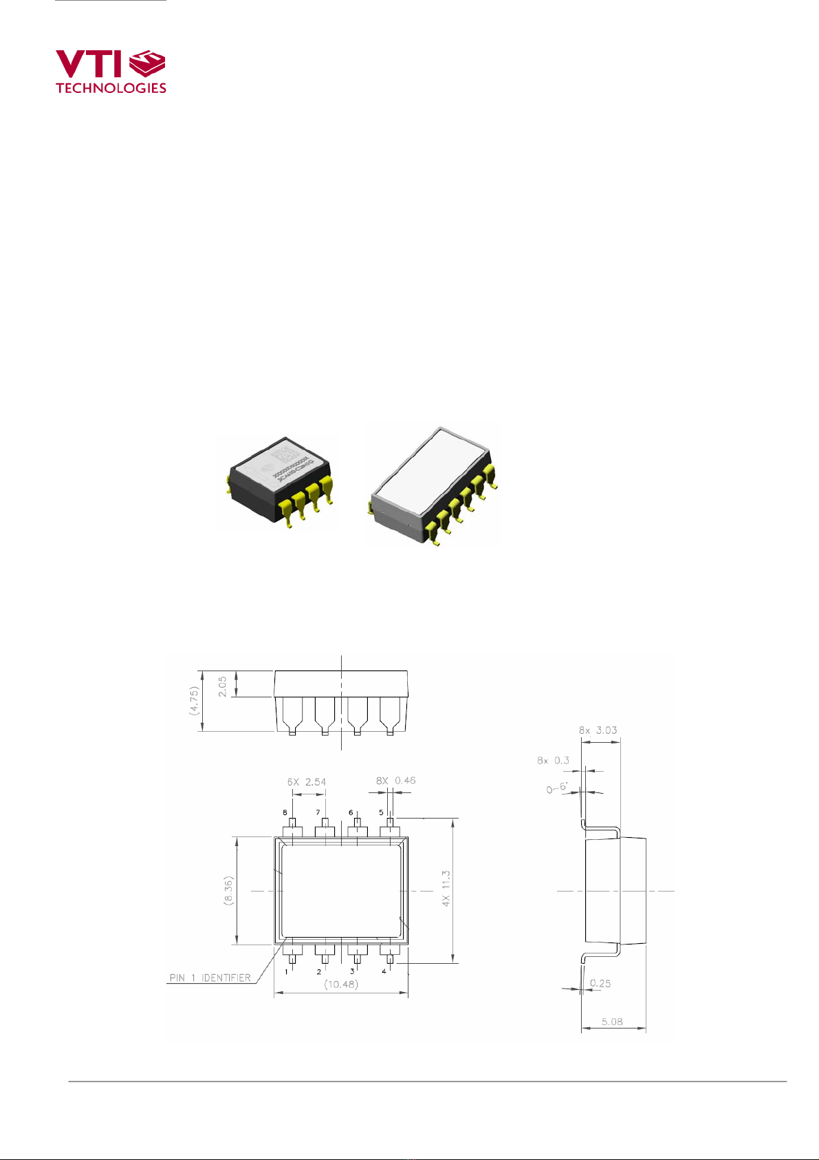
presented in Figure 5.
DIL packages must be placed onto the PCB accurately according to their geometry. The reference
planes are the bottom and the side walls of the component. Placement should be done with
modern automatic component pick & place machinery using vision systems. Recognition of the
packages automatically by a vision system enables correct centering and orientation of packages.
Pin #1 is indexed by a dot mark on the component lid as illustrated in figure 5.
In the case of double sided SMT assembly, it should be noted that VTI's components are relatively
heavy and they should be glued on the PCB if they are located on the bottom side of the PCB
during the second solder reflow process. VTI's does not recommend any specific glue for this
purpose. Some of VTI's customers have used standard epoxy based SMD adhesives.
5.6 Reflow soldering
A forced convection reflow oven is recommended to be used for soldering DIL components. IR-
based reflow ovens are not generally suitable for lead-free soldering. Figure 8 presents a general
forced convection reflow solder profile and it also shows the typical phases of a reflow process.
The reflow profile used for soldering the DIL package should always follow the solder paste
manufacturer's specifications and recommended profile. If washing process is done after the
soldering process, it must be noted that ultrasonic agitation wash after reflow is not allowed
for VTI's DIL packaged MEMS components. As mentioned before (section 5.2) a no-clean paste
is recommended.