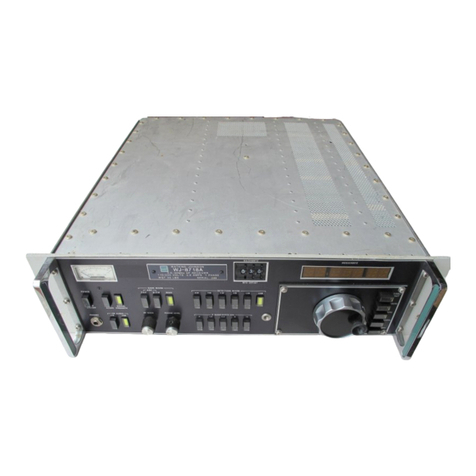
Watkins-Johnson Company WJ-8718-19/FE User manual

10/83
r
INSTRUCTION
MANUAL
FOR
WJ-8718-19/FE
HF
RECEIVER
This
document
and
subject
matter
disclosed
herein
are
proprietary
items
to
which
Watkins-
Johnson
Company
retains
the
exclusive
right
of
dissemination,
reproduction,
manufacture
and
sale.
This
document
is
provided
to
the
individual
or
using
organization
for
their
use
alone
in
the
direct
support
of
the
associated
equipment
unless
permission
for
further
disclosure
is
expressly
granted
in
writing.
WATKINS-JOHNSON
COMPANY
700
QUINCE
ORCHARD
ROAD
GAITHERSBURG,
MARYLAND
20878

WARNING
This
equipment
employs
dangerous
voltages
which
may
be
fatal
if
contacted.
Exercise
extreme
caution
in
working
with
this
equip
ment
with
any
of
the
protective
covers
removed.

]
CUSTOMER
SERVICE INFORMATION
EQUIPMENT
MALFUNCTIONS
This
unit
was
thoroughly
inspected
and
factory
adjusted
for
optimum
performance
prior
to
shipment.
If
an
apparent
malfunction
is
encountered
after
installation,
verify
that
the
correct
input
signals
are
present
at
the
proper
connectors.
Prior
to
taking
any
corrective
maintenance
action
or
breaking
any
seals,
contact
your
Watkins-Johnson
representative, or
the
Watkins-Johnson
Company
Service
Department
to
prevent
the
possibility
of
voiding
the terms of
the warranty. Contact the Watkins-Johnson
Company
via mail, telephone, wire, or cable at:
Watkins-Johnson Company
Company
Service
Department
700
Quince
Orchard
Road
Gaithersburg,
Maryland
20878-1794
Toll
Call:
(301)
948-7550
Ext.
7201
TELEX:
89-8402
TWX:
710-828-0546
TELEFAX:
(301)
921-9479
EASYLINK:
62928185
If
reshipment
is
necessary,
follow
the
instructions
in
the
following
paragraph
(Preparation for Reshipment or Storage). Do not return the equipment until a Return for
Maintenance Authorization
(RMA)
number has been obtained from
the
Watkins-Johnson
Company's
Customer
Service
Department.
See Item 10 in
the
General
Terms
and Conditions
of
Sale paper (WJ Form # WJ-151-X) for more information on equipment returns.
PREPARATION
FOR
RESHIPMENT
OR
STORAGE
If the unit must be prepared for reshipment,
the
packaging
method should follow
the
pattern
established in
the
original shipment. Use
the
best
packaging
materials
available
to
protect
the
unit during reshipment or
storage.
When
possible, use
the
original packing
container
and cushioning materials. If the original packing materials are not available, use the following
procedure:
1.
Wrap
the
unit
in
sturdy
paper
or
plastic.
2.
Place
the
wrapped
unit
in a
strong
shipping
container
and
place
a
layer
of shock-absorbing
material
(3/4-inch
minimum
thickness)
around
all
sides
of
the
unit
to
provide
a
firm
cushion
and
to
prevent
movement
inside
the
container.

3.
CUSTOMER
SERVICE
INFORMATION
vvnwnVnanJ0*
SemCe'
filJ
0ut
a11
inf
nation
on
the
5x6
I
a?
PnwK
DISCREPANCY
REPORT
card
(WJ
Form
#
WJC-
QA55-0)
that
was
provided
with
the
original
shipment.
Also
ensure
that
the
Return
for
Maintenance
Authorization
(RMA)
number
is
recorded
on
the
card.
If
this
card
is
not
available,
attach a tag to the
unit
containing
the
following
information:
a.
Return
for
Maintenance
Authorization
(RMA)
number.
b.
The
Watkins-Johnson
Type/Model
number
of
the
equipment.
c.
Serial
number.
d.
Date
received.
e.
Date
placed
in
service.
f.
Date
of
failure.
g.
Warranty
adjustment requested,
yes
or
no.
h.
A brief description of the discrepant conditions,
i.
Customer
name and return address,
j. Original Purchase Order/Contract number.
4.
Thoroughly
seal the
shipping
container
and
mark
it
FRAGILE.
5.
Ship
to:
Watkins-Johnson Company
700
Quince
Orchard
Road
Gaithersburg, Maryland 20878-1794
U.S.A
When
storing
the
equipment
for
extended
periods,
follow
the
above
Dackine
instructions
to
prevent
damage
to the
equipment.
The
safe
limits
for
storage
environment
are:
Temperature:
-40
to
+70°C
Humidity:
less
than
95%

WJ-8718-19/FE
HF
RECEIVER
CONTENTS
TABLE
OF
CONTENTS
SECTION
I
GENERAL
DESCRIPTION
Paragraph
Page
1.1
Electrical
Characteristics
1_!
1.2
Mechanical
Characteristics ,'..].
1-2
1.3
Equipment
Supplied
'/'[
1_2
1.4
Equipment
Required
But
Not
Supplied
]]]
1_3
1.5 Optional Equipment 1_3
1.6 WJ-8718-19/FE
HF
Receiver
Specifications
1-3
SECTION
II
INSTALLATION
AND
OPERATION
2.1 Unpacking
and
Inspection
2-1
2.2
Preparation
for
Reshipment
and
Storage
2-1
2.3
Installation
2-1
2.3.1
Input/Output
Connectors
2-1
2.3.1.1
Voltage
Selector/Fuse
Block
and
Line
Cord
Receptacle
(FL1J1)
2-2
2.3.1.2
RF
Input
(A2J1)
2-2
2.3.1.3
Line/Phone
Audio
Out
(J16)
2-2
2.3.1.4
Sync
Serial
I/O
(J14)
2-4
2.3.1.5
Clock
Switch
(S2)
2-4
2.3.1.6
1 MHz
REF
(Jll)
2-4
2.3.1.7
Remote
Input
(232J1)
2-4
2.3.1.8
Monitor
Output
(232J2)
2-4
2.3.1.9
IF
Output
(J12)
2-5
2.3.1.10
ISB/FM
Audio
(J15)
2-5
2.3.1.11
Line
Audio
Level
(Rl)
2-5
2.4
Operation
2-5
2.4.1
Introduction
2-5
2.4.2
Front
Panel
Controls
and
Indicators
2-6
!2.4.2.1 Push On/Off Power (SI) 2-5
2.4.2.2
Meter
(Ml)
2-6
2.4.2.3
Meter
Switch
2-6
2.4.2.4
Scanner
Mode
Switches
2-6
j2.4.2.5 Detection
Mode
Switches 2-6
2.4.2.6
Gain
Mode
Switches
2-6
2.4.2.7
BFO
OFS/THRS
LVL
Display
2-8
2.4.2.8
Fault
Indicators
2-8
2.4.2.9
Tuned
Frequency
Readout
2-8
2.4.2.10
Tune
Switches
2-8
^
2.4.2.11
Tuning
Knob
2-8
2.4.2.12
General
Purpose
Keypad 2-8
iii

C°NTENTS
WJ-8718-19/FE
HF
RECEIVER
IV
TABLE OF
CONTENTS
(Cont'd)
SECTION
II
INSTALLATION
AND
OPERATION
2.4.2.13
Memory
Operations Switches ? o
2.4.2.14
MEM
ADRS
Display
."!!.'.'!.'.'.'.'!.'!!!!.'.'.'!".'" °
2-8
2.4.2.15
Bandwidth
Select
Switches
...
-
2.4.2.16
REMOTE/LOCAL
Switches
] »
2.4.2.17
RF
Gain
Control
..'....'/.'.'..'...............'
2-9
2.4.2.18
Phone
Level
Control
2.4.2.19
PHONES
Jack
,,
[[['.'.'.'.'.'.'.'.'.'.'.'.'.'.'.'.'.'.
\
2-9
2.4.3
Local
Control
Mode
,,,
[[,.
[\['/...[[[[
2-9
2.4.3.1
Local/Remote
Switches
.••!•!!!!!."!
2-9
2.4.3.2
General
Purpose
Keypad
••!..!!!!!."."!
2-10
2.4.3.3 Receiver Operating Parameters
2-11
2.4.4
Memory
Storage and Recall Operations
2-16
2.4.4.1
General
......
1'°
°
°."
2-16
2.4.4.2
Quick
Access
Memory
Channel
!!!!!!.".'.'!!!!!!
2-16
2.4.4.3
Accessing
Numbered
Channels
.......!!!!....'.
2-16
2.4.4.4
Memory
Examination
'.'.'.'.'.'.'.'.'.'.'.'.[
2-18
2.4.5
Memory
Scan
Operations
...!.!.!!!!
2-20
2.4.5.1
General
!!!!!!!
°,
'.'.'.".'.
2-20
2.4.5.2
Special
Purpose
Memory
Channels
2-20
2.4.5.3 Threshold Level 2-21
2.4.5.4
Dwell
Time
."."!!.'!!!!!!!!.'!!!.'.".".'
.!.'!.".*!
2-22
2.4.5.5
Memory
Scan
Control
2-23
2.4.6
Sector
Scan Operation 2-26
2.4.6.1
Sector
Scan
Frequency
Data
2-26
2.4.6.2
Sector
Lockout
2-28
2.4.6.3
Sector
Scan Receiver
Register
Data
...
2-29
2.4.7 Special
Function
Termination
Switch (*) 2-33
2.4.7.1 General 2-33
2.4.7.2
Built
In
Test
Equipment
2-33
2.4.7.3
Special
Master
Mode 2-35
2.4.7.4
Special
Function
Display
2-38
2.4.7.5
Erase
Memory 2-38
2.4.8 Remote
Operation
Via RS-232
Serial
Interface
2-38
2.4.8.1
Preparation
For
Operation
2-38
2.4.8.2
Operation
Via RS-232
Interface
Bus 2-40
2.4.9
Remote
Operation
Via
Synchronous
Serial
I/O 2-52
2.4.9.1
Transfer
To
Receiver
(TTR)
and
Transfer
From
Receiver
(TFR) 2-52
2.4.9.2
Signal
Seek:
Slew
up
and
Signal
Seek:
Slew
Down 2-52
2.4.9.3
Count
Pulses:
Slew up and
Count
Pulses:
Slew Down 2-53

WJ-8718-19/FE
HF
RECEIVER
CONTENTS
TABLE OF CONTENTS
(Cont'd)
SECTION
III
CIRCUIT
DESCRIPTION
Paragraph Page
3.1
Introduction
3_1
3.2
General
Description
3_1
3.2.1
Input
RF
Switching
Section
[]]]
3_1
3.2.2
Frequency
Extender
Section
3_3
3.2.3
RF/IF
Conversion
Section
..*..
3.4
3.2.4
IF/Demodulator
Section
][ 3.5
3.2.5
Synthesizer
Section
3_6
3.2.6
Digital
Control
Section
3-7
3.2.7
Power
Supply
Section
3_8
3.3
Functional
Theory
of
Operation
3-9
3.3.1
Input
RF
Switching
Section
3-9
3.3.1.1
Input
Switch,
FE-A2
3-9
3.3.1.2
RF
Filter,
A2
."."."
3-9
3.3.2
Frequency
Extender,
FE-A1
3-11
3.3.2.1
VHF
Preselector/lst
LO,
FE-A1A1
3-12
3.3.2.2
Input
Converter/2nd
LO,
FE-A1A2
3-12
3.3.3
RF/IF
Conversion
."
3-12
3.3.3.1
Input
Converter
(A3)
3-13
3.3.3.1.1
1st
Mixer,
A3A1
3-13
3.3.3.1.2
2nd
Mixer,
A3A2
3-13
3.3.4
IF/Demodulator
Section
3-13
3.3.4.1
10.7
MHz
Filter
Switch
(A4A1)
3-13
3.3.4.2
10.7
MHz/455
kHz
Converter
(A4A2)
3-15
3.3.4.3
455
kHz
Filter
Switch
(A4A3)
3-16
3.3.4.4
AGC
Amplifier
(A4A6)
3-16
3.3.4.5
455
KHz
Ampl/AM
Detector
(A4A7)
3-16
3.3.4.6
FM/CW/SSB
Detector
(A4A9)
3-16
3.3.4.7
Audio
Amplifier
(A4A10)
3-17
3.3.5
Synthesizer
Section
3-17
3.3.5.1
1st
LO
Synthesizer
(A5A1)
3-18
3.3.5.2
2nd
LO
Synthesizer
(A5A2)
3-18
3.3.5.3
3rd
LO
Synthesizer
(A5A1)
3-18
3.3.5.4
BFO
Synthesizer
(A5A3)
3-18
3.3.5.5
Time
Base
(P/O
A5A1)
3-18
3.3.6
Digital
Control
Section
3-19
3.3.6.1
Synthesizer
Interface/Memory(A6Al)
3-19
3.3.6.2
IF
Interface(A6A2)
3-19
3.3.6.3
Asynchronous
I/O
(A6A3)
3-19
3.3.6.4
Serial
I/O
Buffer
(A6A4)
3-19
3.3.6.5
Sync
Serial
I/O
(A6A5)
3-21
3.3.6.6
Front
Panel
Switch/Encoder
(MFP-Al)
3-21
3.3.6.6.1
Front
Panel
Switchboard
(MFP-AlAl)
3-21
3.3.6.6.2
Front
Panel
Encoder
(MFP-A1A2)
3-21

C0NTENTS
WJ-8718-19/FE
HF
RECEIVER
Paragraph
TABLE OF CONTENTS
(Cont'd)
SECTION
III
CIRCUIT
DESCRIPTION
Page
3.3.7
Power
Supply
Section 3 „.
3.4
Circuit
Descriptions
* ,
21
3.4.1
RF
Input
Filter
(A2)
••••-. -
3.4.2
1st
LO
Synthesizer
(FE-A1
AlAl)
" "
3-23
3.4.3
VCO
(FE-A1A1A2)
!!!!!!!!
3-25
3.4.4 Preselector
(FE-A1A1A3)
•
3-26
3.4.5
2nd
LO
Synthesizer
(FE-A1A2A1)
....WWW
3-27
3.4.6 2nd Converter (FE-A1A2A2) 3-28
3.4.7
1st Converter
(FE-A1A2A3)
•-••••
3.4.8
RF
Input
Switch
(FE-A2)
3-30
3.4.8.1
RF
Input
Switch
(FE-A2A1)
3_30
3.4.9
1
MHz
Filter
(FE-A3)
3.4.10
Input
Converter
(A3)
WWW!!
3-30
3.4.10.1
First
Mixer
(A3A1)
V...........]...].........
3-30
r
3.4.10.2
Second
Mixer
(A3A2)
3-32
3.4.11
10.7
MHz
Filter
Switch
(A4A1)
.'
3-32
3.4.12
10.7
MHz/455
kHz
Converter
(A4A2)
3-34
3.4.13
455
MHz
Filter
Switch
(A4A3)
W.i
3-36
3.4.14
AGC
Amplifier (A4A6) 3-36
3.4.15 455
kHz
Amplifier/AM
Detector
(A4A7) 3-40
3.4.16 FM/CW/SSB
Detector
(A4A9) 3-40
3.4.17 Audio Amplifier (A4A10) 3-43
3.4.18 1st and 3rd
LO
Synthesizer/Time
Base (A5A1) 3-46
3.4.18.1
VCO
(A5A1A1)
3_46
3.4.18.2
1st
and
3rd
LO/Time
Base
(A5A1A2)
."..'.WW'!!!!!
3-46
3.4.19 2nd
LO
Synthesizer
(A5A2) ,3-52
3.4.20 BFO
Synthesizer
(A5A3) 3-55
3.4.21
Synthesizer
Interface/Memory(A6Al)
3-57
3.4.22 IF
Interface
(A6A2) 3-6O
3.4.23
Asynchronous
I/O (A6A3) 3-62
3.4.24
Serial
I/O
Buffer
(A6A4)
!!!!
3-65
3.4.25
Sync
Serial Input/Output
(A6A5)
!!!!!!!!!
3-67
3.4.26
Front
Panel
Switch
Encoder
(MFP-Al)
3-69
3.4.26.1
Front
Panel
Encoder
Board
(MFP-Al
Al)
W.
3-69
3.4.26.2 Front Panel Switch
Board
(MFP-AlA2)
WW!!
3-71
VI

WJ-8718-19/FE
HF
RECEIVER
CONTENTS
TABLE OF CONTENTS
(Cont'd)
SECTION
IV
MAINTENANCE
Paragraph
Page
4.1 General 4-1
4.2 Preventive Maintenance
4_1
4.2.1
Visual
Inspection
!!'.!
4-2
4.2.2
Cleaning
WW
4-2
4.2.3 Lubrication
4_2
4.3
Receiver
Checkout
Procedure
W
4-3
4.3.1
General
WW!!!.!.!.....!
4-3
4.3.2 Test Equipment Required 4_4
4.3.3 Receiver Checkout Procedure Guideliness 4-4
4.3.4 Module
Troubleshooting
Procedures
4_16
4.3.4.1 Procedure Guidelines 4_lg
4.3.4.2
RF
Filter
Testing
and
Troubleshooting
WWW!!!!!!!!
4-17
4.3.4.4
1st
LO
Synthesizer,
FE-A1A1A1,Testing
and
Troubleshooting...!!'.!
4-18
4.3.4.5
VCO,
FE-A1A1A2,
Testing
and
Troubleshooting
4-19
4.3.4.6
Preselector,
FE-A1A1A2,
Testing
and
Troubleshooting ..."..*
4-21
4.3.4.7
2nd
LO
Synthesizer,
FE-A1A2A1,
Testing
and
Troubleshooting
!!
4-22
4.3.4.8 2nd Converter, FE-A1A2A2, Testing and
Troubleshooting
4-23
4.3.4.9
1st
Converter,
FE-A1A2A3,
Testing
and
Troubleshooting
.!!
4-24
4.3.4.10
RF
Switch,
FE-A2,
Testing
and Troubleshooting 4-26
4.3.4.11 1
MHz
Filter,
FE-A3,
Testing
and Troubleshooting 4-27
4.3.4.12
Input
Converter
Testing
and
Troubleshooting
4-27
4.3.4.13
10.7
MHz
Filter
Switch
Testing
and
Troubleshooting
.WW
4-29
4.3.4.14 10.7
MHz/455
kHz
Converter Testing and
Troubleshooting
4-30
4.3.4.15
455
kHz
Filter
Switch Testing and Troubleshooting 4-31
4.3.4.16
AGC
Testing
and
Troubleshooting ..."
4-33
4.3.4.17
455
kHz
Amplifier/AM
Detector
Testing and
Troubleshooting
4-34
4.3.4.18
FM/CW/SSB
Detector
Testing
and
Troubleshooting
4-36
4.3.4.18.1
CW/SSB
Detector
Checkout
Procedure
4-36
4.3.4.18.2
FM
Detector
Checkout
Procedure
4-36
4.3.4.19
Audio
Amplifier
Testing
and
Troubleshooting
4-38
4.3.4.20
1st
LO
Synthesizer
Testing
and
Troubleshooting
4-39
4.3.4.21
2nd
LO
Synthesizer
Testing
and
Troubleshooting
4-41
4.3.4.22 3rd
LO
Synthesizer
Testing
and
Troubleshooting
4-43
4.3.4.23
BFO
Synthesizer testing and Troubleshooting
4-44
4.3.4.24 Time Base
Testing
and
Troubleshooting
4-45
4.3.4.25
Synthesizer/Interface
Testing
and
Troubleshooting
4-47
4.3.4.26 IF
Interface
Testing
and
Troubleshooting
4-50
4.3.4.27 Asynchronous I/O Testing and Troubleshooting 4-52
4.3.4.28 Serial I/O
Buffer,
A6A4,
Testing
and
Troubleshooting
4-53
4.3.4.29 Sync
Serial
I/O,
A6A5,
Testing
and
Troubleshooting
4-54
4.3.4.30
Front Panel Encoder Bd., MFP-Al,Testing and Troubleshooting 4-55
4.3.4.31 Front Panel Audio
Circuits,
Testing and
Troubleshooting
4-56
Vll

r
CONTENTS
WJ-8718-19/FE
HF
RECEIVER
TABLE OF CONTENTS
(Cont'd)
SECTION
IV
MAINTENANCE
Paragraph
page
4.3.5 Parts Replacement Guidelines
4_57
4.3.5.1
Soldering
Techniques
WWW'!!!!
WW
4-57
4.3.5.2
Component
Replacement
!!!
WW'!.'!
W
4-58
4.3.5.3 Realignment
4_5g
4.3.6
Adjustment/Alignment
Procedures
.'!
"
4-59
4.3.6.1
General
WWW!!!!!.!!!
4-59
4.3.6.2
Synthesizer
Alignment
WW
4-59
4.3.6.2.1
1st
LO
Synthesizer
Alignment
!!!!!!!
4-59
4.3.6.2.2
2nd
LO
Synthesizer
Alignment
(A5A2)
4-60
4.3.6.2.3
2nd
LO
Filter
Adjustment
WWW!!
4-63
4.3.6.2.4
3rd
LO
Synthesizer
Alignment
WW!!!!!!!!!.""
4-63
4.3.6.2.5
2
MHz
Time
Base
Adjustment
WWW!!!!!
4-63
4.3.6.2.6
BFO
Synthesizer
Alignment
....WWW.
4-64
4.3.6.3
Receiver
Alignment
...WWW
4-64
4.3.6.3.1
Input
Converter
Alignment
WW
4-64
4.3.6.3.2
10.7
MHz
Filter
Switch
Adjustment
WW
WW.
WW
4-66
4.3.6.3.3
455
MHz
Amplifier/AM Detector Response Alignment 4-67
4.3.6.3.4
455
kHz
Amplifier/AM
Detector
Gain
Adjustment
4-69
4.3.6.3.5
FM
Discriminator
Alignment
'
4.70
4.3.6.3.6
LED
Intensity
Adjustment
....WW
4-73
4.3.6.4
Frequency
Extender
Alignment
4-73
4.3.6.4.1
1st
LO
Synthesizer,
FE-A1A1A1, Alignment 4-73
4.3.6.4.2
Preselector,
FE-Al
Al
A3,
Alignment
4-74
4.3.6.4.3
2nd
LO
Synthesizer,
FE-A1A2A1, Alignment 4-75
SECTION
V
REPLACEMENT
PARTS
LIST
5.1 Unit Numbering
Method
5_1
5.2
Reference
Designation
Prefi
5-1
5.3 List of
Manufacturers
5_1
5.4
Parts
List
.......WWW
5-5
5.5
Revision
Level
5.5
5.6
Type
WJ-8718-19/FE
HF
Receiver
WW!!!!!!!!!!!!!!!!
5-6
5.6.1
Type
72640
Power
Distribution
5-15
5.6.2 Type 791616-1 RF
Filter
, 5-17
—
5.6.2.1
Part
280093 30
MHz
Low
Pass
Filter
5-19
i.6.3
Type
791592-8
Input
Converter
!W
5-21
5.6.3.1
Part
370611-7
1st
Mixer,
1st
IF , 5-23
5.6.3.2 Part 370646-7 2nd Mixer, 2nd IF 5-25
5.6.4 Type 794278-1
Frequency
Extender
5-28
viii

WJ-8718-19/FE
HF
RECEIVER
CONTENTS
TABLE OF CONTENTS
(Cont'd)
SECTION
V
REPLACEMENT
PARTS
LIST
Paragraph page
5.6.4.1 Type 794315-1
VHF
Preselector/lst
LO
Assembly 5-30
5.6.4.1.1 Type 370689-1
1st
LO
Synthesizer
5_32
5.6.4.1.2
Type
370690-1
VCO
WW!
5-35
5.6.4.1.3
Type
794274-1
Preselector
WWW!!!!!!!
5-38
5.6.4.2
Type
794316-1
Input
Converter/2nd
LO
Assembly
...WW
5-41
5.6.4.2.1
Type
794270-1 2nd
Local
Oscillator
5-43
5.6.4.2.2
Type
270907-1 2nd LO
Converter
5_46
5.6.4.2.3
Type
270901-1
1st
Converter
5-48
5.6.4.3
Type
794276-1
RF
Input
Switch
W
5-50
5.6.4.3.1
Type
270935-1 RF
Input
Switch
PW
Assembly
5-52
5.6.4.4
Type
794327-1 1
MHz
Filter
5-54
5.6.5
Type
791569-1
IF
Motherboard
!!
5-56
5.6.5.1
Type
791594-6
10.7
MHz
Filter
Switch
!!!!!
5-58
5.6.5.2
Type
794254-1
10.7
MHz/455
kHz
Converter
!!
5-62
5.6.5.3
Type
791595-9 455 kHz
Filter
Switch
5-66
5.6.5.6
Type
796175-1
AGC
Amplifier
5-69
5.6.5.7
Type
726002-2 455 kHz Amplifier/AM
Detector
5-73
5.6.5.8
Type
791599-4
FM, CW,
<5c
SSB
Detector/Audio
5-77
5.6.5.9
Type
7459
Audio
Amplifier
5-80
5.6.6
Type
791570-1
Synthesizer
Motherboard
5-83
5.6.6.1
Type
791630-1
1st
and
3rd
LO
Synthesizer
5-85
5.6.6.1.1
Type
791629
1st
LO VCO
Assembly
5-88
5.6.6.1.2
Part
34750
1st
LO
Voltage
Controlled
Oscillator
5-90
5.6.6.1.3
Type
791600-1
1st
&
3rd
LO
Synthesizer
5-94
5.6.6.2
Type
791601
2nd
LO
Synthesizer
5-100
5.6.6.3
Type
791576-1
BFO
Synthesizer
5-106
5.6.7
Type
791580-1
I/O
Motherboard
5-109
5.6.7.1
Type
794275-X
Synthesizer
Interface/Memory
5-111
5.6.7.2
Type
796032-1
IF
Interface
5-114
5.6.7.3
Type
796037
Asynchronous
I/O
5-117
5.6.7.4
Type
794300-1
Serial
I/O
Buffer
5-120
5.6.7.5
Type
794255-1
Sync
Serial
I/O
5-122
5.6.8
Type
796013-5
Front
Panel
Motherboard
5-124
5.6.8.1
Type
796056-1
Front
Panel
Encode
5-126
5.6.8.2
Type
796057-5
Front
Panel
Switch
Board
5-129
5.6.9
Type
791202-5
Encoder
Assembly
5-133
IX

CONTENTS
WJ-8718-19/FE
HF
RECEIVER
TABLE
OF
CONTENTS
(Cont'd)
LIST
OF
ILLUSTRATIONS
SECTION
I
Figure Page
1-1 WJ-8718-19/FE
HF
Receiver
1_0
SECTION
II
2-1 Receiver Rear Panel Input/Output
Connectors
2-3
2-2 Receiver
Front
Panel
Controls
and
Indicators
2-7
2-3
Master/Slave
Setup
[
2-36
2-4
Daisy
Chain
Configuration
WW!
2-41
2-5
Byte
Structure
.WW
2-44
2-6
DTR
and
DFR
Format
WWW!!!!!!!!!!
2-54
2-7
TTR
Timing
W W W W
2-55
2-8
TRF
Timing
WWW!!!!!!!
2-56
2-9
Signal
Seek:
SLEW
Up
Timing
WW!!!!!!!!!!!!!!!!!!!!
2-57
2-10
Count
Pulses:
SLEW
Down
Timing
W!
2-58
SECTION
III
3-1 Receiver Overall Block Diagram 3_2
3-2 Input Switching Block Diagram
3_10
3-3
Frequency
Extender
Block
Diagram
WW
3-11
3-4 RF/IF Conversion Block Diagram
3_12
3-5 IF/Demodulator Section Block Diagram 3-14
3-6
Synthesizer Section
Block
Diagram
!!!
3-17
3-7
Digital
Control
Section
Block
Diagram
WWW!
3-20
3-8
Power
Supply
Section
Functional
Block
Diagram
"
3-22
3-9
1st
LO
Synthesizer
Block
Diagram
""
3-24
3-10
VCO
Block
Diagram
!!!!!!!!
3-25
3-11
Preselector
Block
Diagram
!!!!!!!!!!
3-26
3-12
2nd
LO
Synthesizer
Block
Diagram
WW!
3-27
3-13
2nd
Converter
Block
Diagram
WW
3-28
3-14
1st Converter Block
Diagram
,...
3-29

WJ-8718-19/FE
HF
RECEIVER
CONTENTS
Figure
TABLE OF CONTENTS
(Cont'd)
LIST
OF
ILLUSTRATIONS
SECTION
III
Page
3-15
Input Converter Functional Block
Diagram
3_31
3-16
10.7
MHz
Filter
Switch
Functional
Block
Diagram
!.!!!!!!!!!!
3-33
3-17
10.7
MHz/455
kHz
Converter
Functional
Block
Diagram
WWW
3-35
3-18
455
kHz
Filter
Switch
Functional
Block
Diagram
WW
3-37
3-19
AGC
Amplifier
Functional
Block
Diagram
WWW!!!!
3-38
3-21
455
kHz
Amplifier/AM
Detector
Functional
Block
Diagram!!."!!!'."
3-41
3-22
FM/CW/SSB
Detector
Functional
Block
Diagram
WW
3-42
3-23
Audio
Amplifier
Functional
Block
Diagram
WWW!!!!!!
3-44
3-23
1st
LO
Functional
Block
Diagram
WWW"
3-47
3-24
2nd
LO
Functional
Block
Diagram
WWW!!!!!!
3-48
3-25
3rd
LO
Functional
Block
Diagram
WW!!!!!!!!!!!!!
!!
3-49
3-26
!-it-.^->
3-27
3-28
3-29
BFO
Functional
Block
Diagram
3_53
Time
Base
Circuits
Functional
Block
Diagram!!!!!!!!!!!!!!!!!!!!!
3_56
Synthesizer
Interface/Memory
Block
Diagram
..WWW!
3-58
IF
Interface
Block
Diagram
WWW
3-61
3-30
Asynchronous
I/O
Block
Diagram
WWW
3-63
3-31
Serial
I/O
Buffer
Block
Diagram
•••...
3-32
Sync
Serial
I/O
Block
Diagram
WW
.WW
3-68
3-33
Front
Panel
Encoder
Block
Diagram
...WWW!
3-70
SECTION
IV
4-1 Receiver Checkout Procedure, Test Setup
4_6
4-2 Input Converter Alignment Test Setup 4.55
4-3
10.7
MHz
Filter
Switch
Adjustment,
Test
Setup
WW!!
4-66
4-4
455
kHz
Amplifier/AM
Detector
Response
Alignment,
Test
Setup!.'!!
4-68
4-5
455
kHz
Amplifier/AM
Detector Response Alignment, Typical
Response
4-69
4-6
4^5
kHz
Amplifier/AM Detector
Gain
Adjustment, Test Setup 4-70
4-7
FM
Discriminator Alignment, Test Setup 4-72
4-8
FM
Discriminator
Alignment,
Typical
Response
.WW!
4-72
4-9
Preselector
Alignment,
Test
Setup
W!
4-74
xi

CONTENTS
WJ-8718-19/FE
HF
RECEIVER
Figure
TABLE
OF CONTENTS
(Cont'd)
LIST
OF
ILLUSTRATIONS
SECTION
V
Page
5-1 WJ-8718-19/FE
HF
Receiver,
Front
Panel,
Location
of
Components....
5_7
5-2 WJ-8718-19/FE
HF
Receiver,
Rear
Panel,
Location
of Components 5_7
5-3
WJ-8718-19/FE
HF
Receiver,
Top
View,
•••••••••••••
........
Location
of Components 5_o
5-4 WJ-8718-19/FE
HF
Receiver, Bottom View,
Location
of Components 5-12
5-5
Type
76240
Power
Distribution,
Location
of
Components
5-16
5-6
Type
791616-1
Input
Filter
(A2),
Location
of Components 5-18
5-7 Part 280093 30
MHz
Low
Pass
Filter
(A2A1),
Location
of
Components 5-20
5-8
Type
791592-8
Input
Converter
(A3),
Location
of Components 5-22
5-9
Part
370611-7
1st
Mixer,
1st
IF (A3A1),
Location
of Components 5-24
5-10
Part
370646-7 2nd Mixer, 2nd IF (A3A2),
Location
of
Components
5_26
5-11 Type 794278-1
Frequency
Extender
(FE-A1),
Location
of
Components
5-29
5-12 Type 794315-1
VHF
Preselector/lst
LO
Assembly (FE-A1A1),
Location
of
Components
5-31
5-13
Type
370689-1
1st
LO
Synthesizer
(FE-A1A1A1),
Location
of
Components
5-34
5-14
Type
370690-1
VCO
(FE-A1A1A2),
Location
of
Components
5-37
5-15
Type
794274-1
Preselector
(FE-A1A1A3),
Location
of
Components
5-40
5-16 Type 794316-1
Input
Converter/2nd
LO
Assembly
(FE-A1A2),
Location
of
Components
5-42
5-17
Type
794270-1 2nd
Local
Oscillator
(FR-A1A2A1),
Location
of
Components
5-45
5-18
Type
270907-1 2nd LO
Converter
(FE-A1A2A2),
Location
of
Components
5-47
5-19
Type
270901-1
1st
Converter
(FE-A1A2A3),
Location
of
Components
5-49
5-20
Type
794276-1
RF
Input
Switch
(FE-A2),
Location
of
Components
5-51
5-21 Type 270935-1 RF
Input
Switch
PW
Assembly
(FE-A2A1),
Location
of
Components
5-53
-22
Type
794327-1 1
MHz
Filter
(FE-A3),
Location
of
Components
5-55
5-23
Type
791569-1 IF
Motherboard
(A4),
Location
of
Components
5-57
xn

WJ-8718-19/FE
HF
RECEIVER
CONTENTS
TABLE
OF
CONTENTS
(Cont'd)
LIST
OF
ILLUSTRATIONS
SECTION
V
Figure
Page
5-24
Type
791594-6
10.7
MHz
Filter
Switch
(A4A1),
Location
of
Components
5-59
5-25
Type
794254-1
10.7
MHz/455 kHz
Converter(A4A2),
Location
of
Components
5_65
5-26
Type
791595-9
455 kHz
Filter
Switch
(A4A3),
Location
of
Components
5-68
5-26
Type
796175-1
AGC
Amplifier
(A4A6),
Location
of
Components
5_70
5-27 Type 726002-2 455
kHz
Amplifier/AM
Detector
(A4A7),
Location
of Components 5-76
5-28
Type
791599-4 FM,
CW,
and SSB
Detector
(A4A9),
Location
of
Components
5_7g
5-29
Type
7459
Audio
Amplifier
(A4A10),
Location of Components 5-82
5-30 Type 791570-1
Synthesizer
Motherboard
(A5),
Location of Components
5_84
5-31 Type 791630-1 1st and 3rd
LO
Synthesizer/Timebase (A5A1),
Location of Components
5_86
5-32 Type 791629
1st
LO
VCO Assembly (A5A1A1),
Location of Components
5_89
5-33
Part
34750
1st
LO
Voltage
Controlled
Oscillator
(A5A1A1A1)",
'
Location of Components 5-93
5-34 Type 791600-1 1st and 3rd
LO
Synthesizer (A5A1A2),
Location of Components 5-95
5-35 Type
791601
2nd
LO
Synthesizer
(A5A2),
Location of Components
5-101
5-36 Type 791576-1 BFO
Synthesizer
(A5A3),
Location
of
Components 5-107
5-37. Type 791580 I/O
Motherboard
(A6),
Location of Components 5-110
5-38 Type 794275-X Synthesizer Interface/Memory (A6A1),
Location of Components 5-113
5-39 Type 796032-2 IF
Interface
(A6A2),
Location of Components 5-116
5-40 Type 796037
Asynchronous
I/O (A6A3),
Location of Components 5-119
5-41 Type 794300-1
Serial
I/O
Buffer
(A6A4),
Location of Components 5-121
5-42 Type 794255-1 Sync
Serial
I/O (A6A5),
Location
of
Components
5-123
5-43
Type 796013-5 Front Panel Motherboard (MFP-Al),
Location of Components 5-125
5-44
Type
796056-1
Front Panel Encode (MFP-AlAl),
Location of Components 5-127
XJ11

C0NTENTS
WJ-8718-19/FE
HF
RECEIVER
Figure
5-45
TABLE
OF
CONTENTS
(Cont'd)
LIST
OF
ILLUSTRATIONS
SECTION
V
Page
Type
796057-5
Front
Panel
Switch
Board
(MFP-A1A2)
Location
of
Components
,
5-46
Type
791202-5
Encoder
Assembly
(MFp"a2)','
°°
Location
of
Components
5-133
SECTION
VI
l'l
TYPe
lllllt'1
inpUt
Filter
(A2),
Schematic
Diagram
380082
6-3
6-2
Type
794278-1
Frequency
Extender
(FE-A1),
Schematic
Diagram 370820
6-3
Type
794315-1
VHF
Preselector/lst'
LO*
AssemblV
'(FE-A1A1)'
Schematic
Diagram 470632
C6-4
Type
370689-1
1st
LO
Synthesizer
(FE-AIAIAI)'
Schematic
Diagram 470466
6-5 Type
370690-1
VCO
(FE-A1A1A2)
Schematic Diagram
470470
6-6
Type
794274-1
Preselector
(FE-A1A1A3)"
Schematic
Diagram
470468
6-7
Type
794316-1
Input
Converter/2nd
LO
Assembly
(FE-A1A2)
Schematic Diagram
370706
6-8
Type
794270-1
2nd
Local
Oscillator'
(FE-A1A2
Al)
'
Schematic
Diagram 470633
6-9
Type
270907-1
2nd
LO
Converter
(FE-A1A2A2)
Schematic Diagram
370819
6-10
Type
270901-1
1st
Converter
(FE-A1A2A3)'
Schematic Diagram
370818
6-11
Type
794276-1
RF
Input Switch (FE-A2)
Schematic
Diagram 370701
6-12
Type
794327-1
1
MHz
Filter (FE-A3)'
""""
° c "
Schematic
Diagram
271039
fi
9C-
6-13
Type
791592-1
Input
Converter
(A3),
••••••••
Schematic
Diagram
570202
.
fi
97
6-14
Type
791569-1
IF
Motherboard
(A4)
° ^"
©-•"
Schematic
Diagram
570202
fi
9q
6-15
Type
791594-6
10.7
MHz
Filter
Switch
(A4A1)!
" " "
Schematic
Diagram
480103
fi
?1
6-16
Type
794254-1
10.7
MHz/455
kHz
Converter''(A4A2)
r
Schematic
Diagram
380215
'
fi
^
-17
Type
791595-9
455
kHz
Filter
Switch
(A4A3),"
Schematic
Diagram
43561
'
6_35
xiv
6-11
6-13
6-15
6-17
6-19
6-21
6-23

WJ-8718-19/FE
HF
RECEIVER
CONTENTS
TABLE
OF
CONTENTS
(Cont'd)
LIST
OF
ILLUSTRATIONS
SECTION
VI
Figure
Page
6-18
Type
796175-1
AGC
Amplifier
(A4A6),
Schematic
Diagram
43229
6-37
6-19
Type
726002-2
455
kHz
Amplifier/AM
Detector
(A4A7),
Schematic
Diagram
570253
6-39
6-20
Type
791599-4
FM,
CW
6c
SSB
Detector
(A4A9),
Schematic
Diagram
43198
6-41
6-21
Type
7459
Audio
Amplifier
(A4A10),
Schematic
Diagram
43230
6-43
6-22
.
Type
791570
Synthesizer
Motherboard
(A5)
Schematic
Diagram
470518
6-45
6-23
Type
791630-1
1st
6c
3rd
LO
Synthesizer/Time
Base
(A5A1),
Schematic
Diagram
43305
6-47
6-24
Type
791629
1st
LO/VCO
Assembly
(A5A1A1),
Schematic
Diagram
51198
6-49
6-25
Type
791600-1
1st
6c
3rd
LO
Synthesizer
(A5A1A2),
Schematic
Diagram
61247
(Sheet
1
of
2)
6-51
6-25
Type
791600-1
1st
6c
3rd
LO
Synthesizer
(A5A1A2),
Schematic
Diagram
61247
(Sheet
2
of
2)
6-53
6-26
Type
791601
2nd
LO
Synthesizer
(A5A2),
Schematic
Diagram
61256
6-55
6-27
Type
791576-1
BFO
Synthesizer
(A5A3),
Schematic
Diagram
51183
6-57
6-28
Type
791580
I/O
Motherboard
(A6)
Schematic
Diagram
470519
6-59
6-29
Type
794275-X
Synthesizer
Interface
(A6A1),
Schematic
Diagram
570208
6-61
6-30
Type
796032
IF
Interface
(A6A2),
Schematic
Diagram
570239
6-63
6-31
Type
796037
Asynchronous
I/O
(A6A3),
Schematic
Diagram
470800
6-65
6-32
Type
794300-1
Serial
I/O
Buffer
(A6A4)
Schematic
Diagram
470496
6-67
6-33
Type
794255-1
Sync
Serial
I/O
(A6A5)
Schematic
Diagram
470455
6-69
6-34
Type
796013-5
Front
Panel
Motherboard
(MFP-A1)
Schematic
Diagram
680028 6-71
6-35
Type
796056-1
Front
Panel
Encode
(MFP-A1A1)
Schematic
Diagram
680029
6-73
6-36
Type
796057-5
Front
Panel
Switch
Board
(MFP-A1A2)
Schematic
Diagram
580049
6-75
6-37 WJ-8718-19/FE HF
Receiver
Main
Chassis,
Schematic
Diagram
570203
6-79
xv

CONTENTS
WJ-8718-19/FE
HF
RECEIVER
TABLE
OF CONTENTS
(Cont'd)
LIST
OF
TABLES
Table
Page
Section
I
1-1 Type WJ-8718-19/FE
HF
Receiver, Specifications 1-4
Section
II
2-1
Termination Switches 2-10
2-2
Threshold
Data
Codes
2-21
2-3
Sector
Scan
Frequency
Data
Storage..!!!." »•••..-.
2-4
Group
1
Switch
Codes
!!!!!!!!!!!!!!!!'
2-34
2-5
Group
2 Switch
Codes
2-6
Baud
Rate
Codes
!!!!!!!!!!!!!!!!!!!!!!
2-39
2-7
Switch
Assembly
(S2)
Functions
!!!!!!!!!!!!!!!!!!!!!!!!!!!!
2-40
2-8
Receiver
Address
Codes
!!!!!--
2-40
2-9
RS-232
Connector
Pin
Ass
ignments
!!!!!!!!!!!!!!!!!!!!!!!!
2-42
2-10
Receiver Address Byte
"°
'
""c
'" "' °
2-11
DID
Byte
!!!!!!!
°"'.'.!!'"
°!"
*"
°°°
°"
°°
°'°'
u
2-20
2-21
2-46
2-12
Register Parameter Data 2
48
2-13
Tier
2
Access
Byte
!!!!!!!!!!!!!!!!
2-49
2-14
Tier
2,
Page
1
Byte
1!!!!!!!!!!!!!!!
?-4Q
2-15
Tier
2,
Page
1
Byte
2
2-49
2-16
Full
Status
Monitor
.!!..!!
2-50
2-17
Bandwidth/Gain/Detection
Mode
Monitor
!!!!!!!!!!!!!!!!!!!
2-50
2-18
Address
15
Receiver
Parameters
2-50
2-19
Command
Parameters
to
Address
4
Receiver
!!!!!!!
2-50
Full
Status
Command
!!!!!!!!!!,!
2-51
Command
BFO
Frequency 2-51
2-22
Tier 2 Access
Format
2-5i
Section
III
3-1
2nd
and
3rd
IF
Bandwidth
Selection
3_15
3-2
Detect
ion
Mode
Select
ion
!!!!
°
3-15
xvi

WJ-8718-19/FE
HF
RECEIVER
OONTENTS
TABLE
OF
CONTENTS
(Cont'd)
LIST
OF
TABLES
Section
IV
Table
Page
4-1
Preventive
Maintenance Schedule
4_1
4-2 Test
Equipment
Required
4_4
4-3
WJ-8718-19/FE
Series
HF
Receiver
Checkout
Procedure
...!!!!!!!!!!!
4-7
4-4 WJ-8718-19/FE
HF
Receiver
Troubleshooting
Procedures
4-11
4-5
1st
LO
Synthesizer Fault Isolat
ion
Chart
"
4-19
4-6
VCO
Fault
Isolation
Chart
!!!!!
4_2o
4-7
Preselector
Fault
Isolation
Chart
!!!!!!
4-22
4-8
2nd
LO
Synthesizer
Fault
Isolation
Chart
!!!!!!!!!
4-23
2nd
Converter
Fault
Isolation
Chart
!!!!!!!!
4-24
1st
Converter
Fault
Isolation
Chart
!!!!!!!!!!
4-25
Input
Converter
Fault
Isolation
Chart
!!!!!!!!
4-28
10.7
MHz
Filter
Switch
Fault
Isolat
ion
Chart
!!!!!!!!!
4-30
4-13
10.7
MHz/455
kHz
Converter
Fault Isolat
ion
Chart
!!!!!!!!
4-31
4-14
455
kHz
Filter
Switch
Fault
Isolat
ion
Chart
!!!!!!!
4-32
PGZ
Fault
Isolat
ion
Chart
!!!!!!!!!
4-34
Amplifier/AM
Detector
Fault
Isolat
ion
Chart
!!!!!!!!!!!!!
4-35
FM/CW/SSB
Detector
Fault Isolat
ion
Chart
!!!!!!!!
4-37
Audio
Amplifier Fault
Isolation
Chart
...
4-19
VCO
Band
Select
'
7JJ
4-20
1st
l£)
Frequency
Chart
1st
LO
VCO
Fault
Isolat
ion
Chart
!!!!!!!!!!!!!!!!!!!!
4-41
32
MHz
Loop
Fault
Isolat
ion
Chart
!!!!!!!!!!!
4-42
Programmable
Loop
Fault
Isolat
ion
Chart
!!!!!!!!!!
4-42
Oit
put
Loop
Fault
Isolat
ion
Chart
!!!!!!!!!
4-43
3rd
LO
Fault Isolation Chart
BFO
Fault
Isolation
Chart
!!!!!!!!!!!!!!!!!
4-45
Time
Base
Frequency
Chart
!!!!!!!!!!!!
4-46
Microcontroller
Input
Signal
Check
!!!!!!!!!!!!!
4-47
Microcontroller
Bus
Activity Check
.............
cpu
i/o
signal
check
!!!!!!!!!!!!!!!!!!!
4-48
Synthesizer
Interface
Frequency
Outputs
!!!!!!!!!!!
4-49
IF
Interface
Control
Signal/Data
Activity
Check
!!!!
4-50
IF
Interface
Voltage
Table
!!!!
4-51
UART
Control
Signal/Data
Activity
Check..!!!!!!!!!!! "
4_52
I/O
Signal
Activity
Check
!!!!!!!!!!!
4-53
Data
Signal
Activity
Check
!!!!!!!!!!!!!!!
4-54
Signal/Data
Activity
Check
!!!!!!!!!!!!!!
4-55
VCO
Alignment
Parameters
!!!!!!!!!!!!!
4-59
Loop
Test
Point
Voltages
!!!!!!!!!!!!!!!!!!!
4-62
2nd
LO
Synthesizer
Tuning
Parameters
!!!!!!!!!
4-62
4-9
4-10
4-11
4-12
4-15
4-16
4-17
4-18
4-41
4-22
4-23
4-24
4-25
4-26
4-27
4-28
4-29
4-30
4-31
4-32
4-33
4-34
4-35
4-36
4-37
4-38
4-39
4-40
xvii

GENERAL
DESCRIPTION
r
WJ-8718-19/FE
HF
RECEIVER
Figure 1-1. WJ-8718-19/FE
HF
Receiver
1-0
Table of contents
Other Watkins-Johnson Company Receiver manuals
Popular Receiver manuals by other brands

Denon
Denon RC-7001RCI - Remote Control RF/IR Base... owner's manual
DX Engineering
DX Engineering DXE-RFS-SYS-3P manual
Sony
Sony HBD-E570 Service manual
PCB Piezotronics
PCB Piezotronics 010F05 Installation and operating manual
Wyrestorm
Wyrestorm MX-0404-HDBT-H2 quick start guide
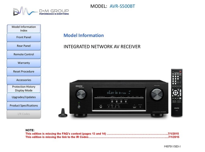
DM Group
DM Group AVR-S500BT manual
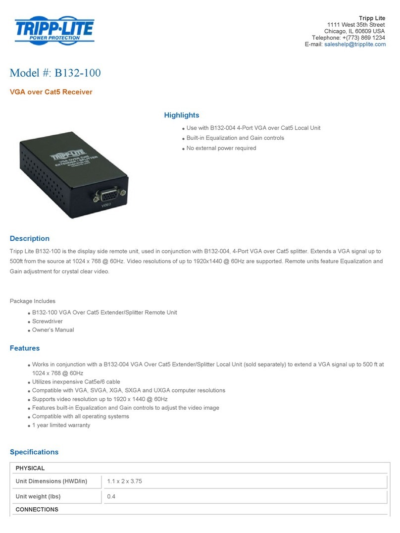
Tripp Lite
Tripp Lite B132-100 Specifications
Paradox
Paradox Liberator 9000 installation manual
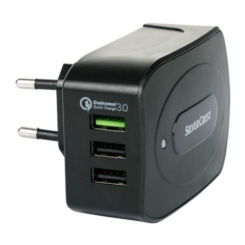
Silvercrest
Silvercrest SLQC 3.0 A1 operating instructions

JVCKENWOOD
JVCKENWOOD KMM-BT408 instruction manual
Ultra Plus
Ultra Plus 780 miCro-PVR user manual
GiBiDi
GiBiDi DOMINO DRS4332 Instructions for installations
