www.teamWavelength.com© 2001-2013
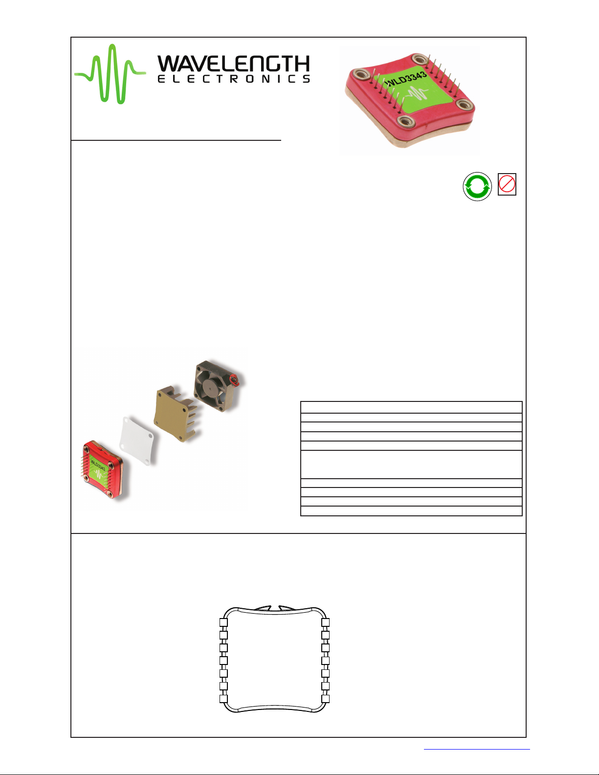
WLD3343
PAGE 3
WLD3343-00400-O
Supply Voltage (Voltage on Pin 14)
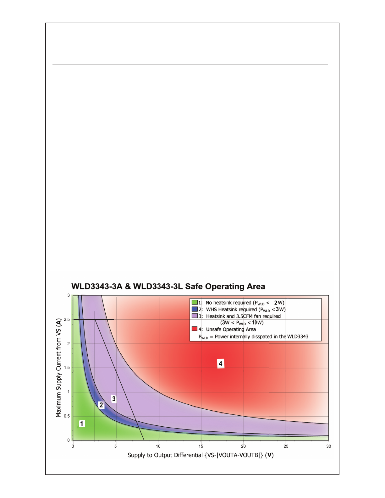
Output Current (See SOA Chart)
Power Dissipation, TAMBIENT = +25˚C
Operating Temperature, case [2]
Storage Temperature
Weight
ELECTRICAL AND OPERATING
SPECIFICATIONS
Volts DC
Amperes
Watts [1]
˚C
˚C
oz
UNITVALUE
+4.5 to +12.5
2.2 or 3
9
- 40 to + 85 [3]
- 65 to +150
0.6
VDD
ILD
PMAX
TOPR
TSTG
WLD3343
ABSOLUTE MAXIMUM RATINGS
RATING SYMBOL
Amps
Volts
Volts
Volts
Volts
Volts
Volts
Volts
Volts
nsec
nsec
MHz
Seconds
Seconds
mA
ppm
%
%
3
3.0
10.0
200
2.2
200
10.6
10.4
10.1
460
320
2.0
(Depends on PD BW)
0.24
0.01
0
OUTPUT
Current, peak, see SOA chart
Compliance Voltage, Laser Diode Load
Compliance Voltage, Laser Diode Load
Compliance Voltage, Laser Diode Load
Compliance Voltage, Laser Diode Load
Compliance Voltage, Laser Diode Load
Compliance Voltage, Laser Diode Load
Compliance Voltage, Laser Diode Load
Compliance Voltage, Laser Diode Load
Rise Time
Fall Time
Bandwidth
Bandwidth
Slow Start - Delay
Slow Start - Ramp
Leakage Current [4]
CONSTANT CURRENT CONTROL
Short Term Stability, 1 hour
CONSTANT POWER CONTROL
Short Term Stability, 1 hour
Long Term Stability, 24 hours
WLD3343-2A UNITSTEST CONDITIONSPARAMETER
ILD = 100 mA, 5 V
ILD = 1.0 Amp, 5 V
ILD = 2.0 Amps, 5 V
ILD = 3.0 Amps, 5 V
ILD = 100 mA,12 V
ILD = 1.0 Amp,12 V
ILD = 2.0 Amp,12 V
ILD = 3.0 Amp,12 V
ILD= Full Scale
ILD= Full Scale
Constant Current, Sine Wave
Constant Power
TAMBIENT = 25˚C
TAMBIENT = 25˚C
TAMBIENT = 25˚C
Notes:
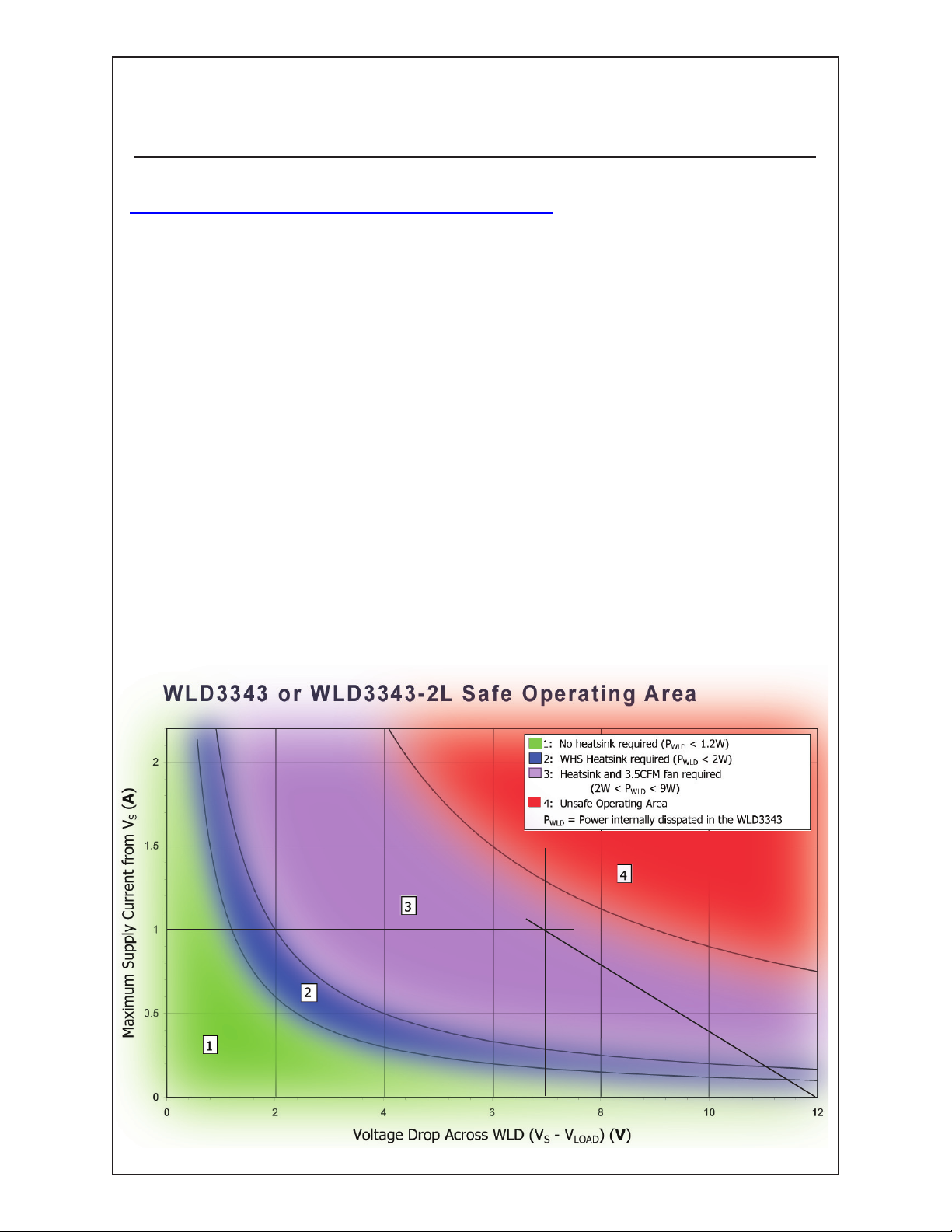
[1] In the WLD3343 and WLD3343-2L models, internal power dissipation is 1.2 W (without heatsink), 2 W (with
heatsink), and 9 W (with heatsink and fan). In the WLD3343-3A and WLD3343-3L models, internal power dissipation
is 2 W (without heatsink), 3 W (with heatsink), and 10 W (with heatsink and fan).
[2] With Revision D forward of the WLD3343, an internal thermostat has been added to activate Shutdown (SHD)
when the internal temperature exceeds 105˚C. The output will be re-enabled after a 250 to 300 msec slow-start once
the internal temperature drops below 95˚C.
[3] Max ambient operating temperature of the WLD3343-3A and WLD3343-3L is 45°C.
[4] Leakage current specification is based on full current set by RSENSE. See page 9 for information on setting the
current range. Minimum turn on current in the 200 mA range is 350 μA. Minimum turn on current in the 2 A range is
12 mA. This specification applies to Rev. E forward.
Noise: To further reduce noise, the WLD3343-2L and WLD3343-3L models are available. Both
are about 2.5 times lower noise than the WLD3343 and WLD3343-3A, respectively. Constant
Power (CP) mode is not available in these models.
0.01
0.05
WLD3343-3A
3.6
3.5
3.0