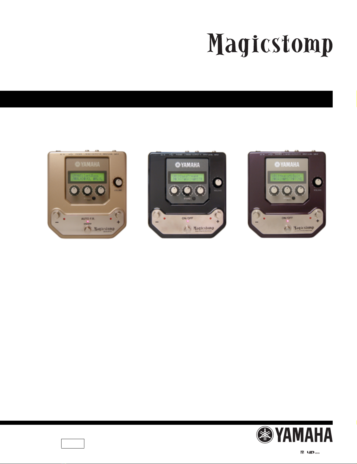
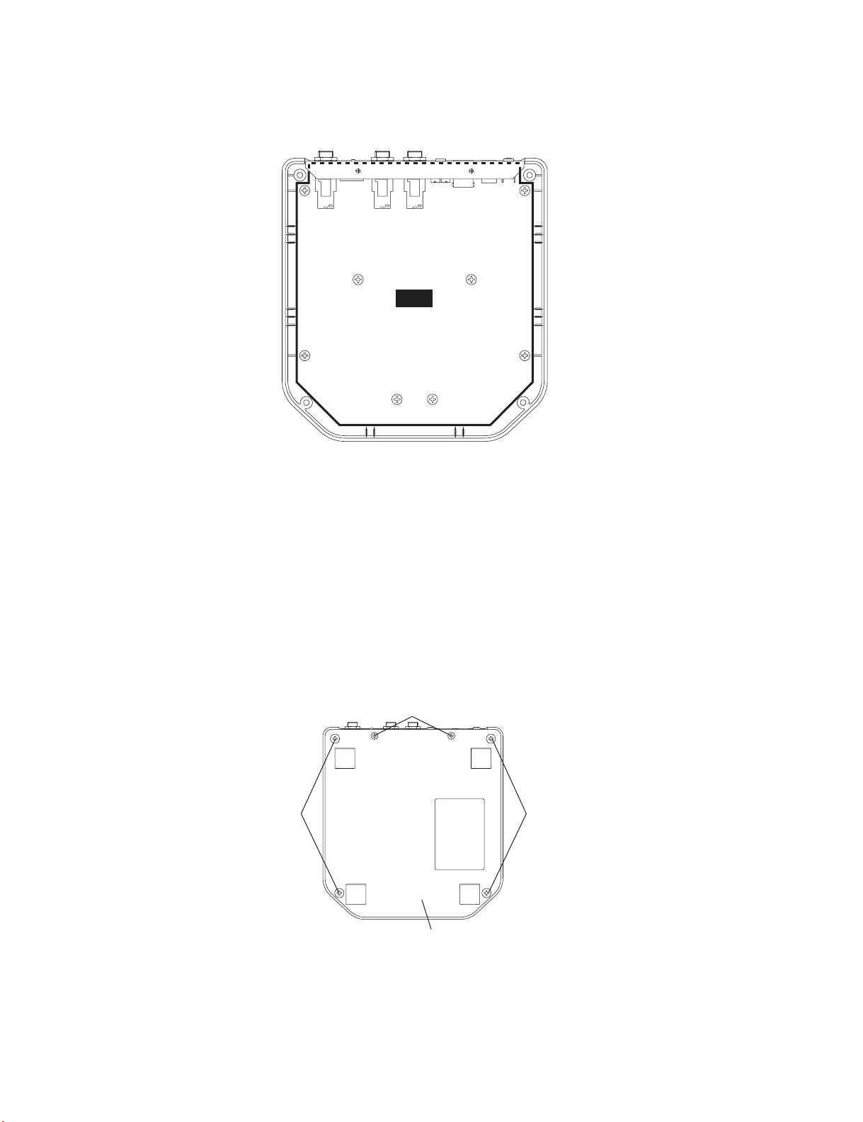
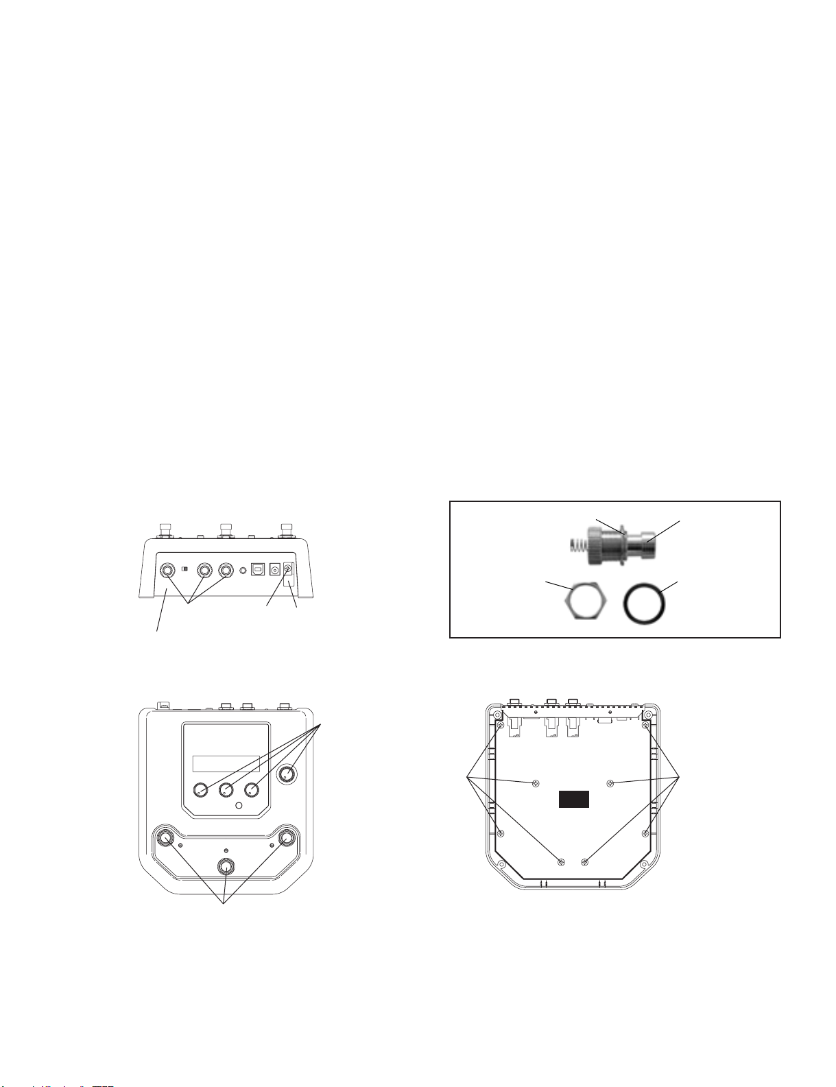
Yamaha UB99A User manual

UB99B
BASS EFFECTS PROCESSOR
SERVICE MANUAL
ACOUSTIC EFFECTS PROCESSOR
BASS EFFECTS PROCESSOR
GUITAR EFFECTS PROCESSOR
UB99A/UB99B/UB99MK2
■CONTENTS(目次)
SPECIFICATIONS(総合仕様)..........................................................3
PANEL LAYOUT(パネルレイアウト)..............................................4
BLOCK DIAGRAM(ブロックダイアグラム)....................................5
CIRCUIT BOARD LAYOUT(ユニットレイアウト)..........................6
DISASSEMBLY PROCEDURES(分解手順)....................................6
LSI PIN DESCRIPTION(LSI 端子機能表)........................................8
IC BLOCK DIAGRAM(IC ブロック図)...........................................11
CIRCUIT BOARD(シート基板図)..................................................12
INSPECTIONS / FACTORY SET(検査 /ファクトリーセット).....14
BACKUP THE USER PATCH DATA
(ユーザーパッチのバックアップ)....................................................25
ERROR MESSAGES(エラーメッセージ).....................................26
PARTS LIST
CIRCUIT DIAGRAM(回路図)
GA 011755 HAMAMATSU, JAPAN
Copyright (c) Yamaha Corporation. All rights reserved. PDF-K366 ’05.03
UB99A
ACOUSTIC EFFECTS PROCESSOR
UB99MK2
GUITAR EFFECTS PROCESSOR

UB99A/UB99B/UB99MK2
2
■WARNING
Components having special characteristics are marked and must be replaced with parts having specification equal to
those originally installed.
印の商品は、 安全を維持する ために重要な部品です。 交換す る場合は、 安全のために必ず指定の部品を ご使用 く だ さ い。
IMPORTANT NOTICE
This manual has been provided for the use of authorized Yamaha Retailers and their service personnel. It has been assumed that basic
service procedures inherent to the industry, and more specifically Yamaha Products, are already known and understood by the users, and
have therefore not been restated.
WARNING : Failure to follow appropriate service and safety procedures when servicing this product may result in personal injury,
destruction of expensive components and failure of the product to perform as specified. For these reasons, we advise
all Yamaha product owners that all service required should be performed by an authorized Yamaha Retailer or the
appointed service representative.
IMPORTANT : This presentation or sale of this manual to any individual or firm does not constitute authorization certification,
recognition of any applicable technical capabilities, or establish a principal-agent relationship of any form.
The data provided is belived to be accurate and applicable to the unit(s) indicated on the cover. The research engineering, and service
departments of Yamaha are continually striving to improve Yamaha products. Modifications are, therefore, inevitable and changes in
specification are subject to change without notice or obligation to retrofit. Should any discrepancy appear to exist, please contact the
distributor’s Service Division.
WARNING : Static discharges can destroy expensive components. Discharge any static electricity your body may have
accumulated by grounding yourself to the ground bus in the unit (heavy gauge black wires connect to this bus.)
IMPORTANT : Turn the unit OFF during disassembly and parts replacement. Recheck all work before you apply power to the unit.
WARNING: CHEMICAL CONTENT NOTICE!
The solder used in the production of this product contains LEAD. In addition, other electrical/electronic and/or plastic (Where applicable)
components may also contain traces of chemicals found by the California Health and Welfare Agency (and possibly other entities) to
cause cancer and/or birth defects or other reproductive harm.
DO NOT PLACE SOLDER, ELECTRICAL/ELECTRONIC OR PLASTIC COMPONENTS IN YOUR MOUTH FOR ANY REASON WHAT
SO EVER!
Avoid prolonged, unprotected contact between solder and your skin! When soldering, do not inhale solder fumes or expose eyes to
solder/flux vapor!
If you come in contact with solder or components located inside the enclosure of this product, wash your hands before handling food.

UB99A/UB99B/UB99MK2
3
■SPECIFICATIONS(総合仕様)
Digital Section
• Digital signal processing effector
• Includes special editor application “Sound Editor for
MAGICSTOMP”
• Patch Select: 2 Modes
• Built-in Chromatic Auto Tuner
Communications
Receive: Parameter Change, Bulk In (1 patch), Bulk
In (99 patch)
Transmit: Bulk Out (99 patch)
Controller/Switch
Knob x4
CONTROL1, 2, 3, VOLUME
Push Switch x4
UB99A: –, +, AUTO F.R./ON/OFF, STORE/EXIT
UB99B/UB99MK2: –, +, ON/OFF, STORE/EXIT
Slide Switch x1
INPUT LEVEL (HIGH/LOW)
Display
16 x 2 character LCD (w/Back light)
LED x 3 (UB99A: –, +, AUTO F.R./ON/OFF)
(UB99B/UB99MK2: –, +, ON/OFF)
Connections
INPUT: Standard Monaural Phone Jack
OUTPUT L/MONO, R: Standard Monaural Phone Jack
PHONES: Mini Stereo Phone Jack
USB
AC IN
A/D Converter
24 bit + 3 bit Floating
D/A Converter 24 bit
Sampling Frequency 44.1 kHz
Memory Allocations Preset:99
User: 99
Input Level/Impedance
INPUT HIGH: –25dBm/1 MΩ
INPUT LOW : –15dBm/1 MΩ
Output Level/Impedance
OUTPUT L/MONO, R: 0dBm/1 kΩ
PHONES L, R: –10 dBm/150 Ω
Power
Exclusive Power Adaptor (AC-10)
AC Output: AC 12 V, 1 A
Power Consumption 12 W
Dimensions (W x H x D) 164 x 62 x 176 mm
(6-7/16” x 2-7/16” x 6-15/16”)
Weight 910 g (2lbs.)
Accessories Power Adaptor (AC-10)
CD-ROM
USB Cable
Owner’s Manual
Patch List
Effect List
デジタル部
•デジ タルシグナルプロセッ シング ・ エフ ェ ク ター
•専用エデ ィ ター ソ フ ト “Sound Editor for MAGICSTOMP”
同梱
•パッチセレク ト : 2 モード
•ク ロ マチ ッ ク オー ト チ ュ ーナー内蔵
通信機能
受信 Parameter Change, Bulk In (1 patch), Bulk In (99
patch)
送信 Bulk Out (99 patch)
コントローラー / スイッチ
ボリューム×4
CONTROL1, 2, 3, VOLUME
プッシュスイッチ×4
UB99A: -, +, AUTO F.R./ON/OFF, STORE/EXIT
UB99B/UB99MK2: -, +, ON/OFF, STORE/EXIT
スライドスイッチ×1
INPUT LEVEL (HIGH/LOW)
ディスプレイ
16 × 2 character LCD ( バ ッ ク ラ イ ト 付き )
LED x 3 (UB99A: -, +, AUTO F.R./ON/OFF)
(UB99B/UB99MK2: -, +, ON/OFF)
接続端子
INPUT (標準フ ォ ンモ ノ ジ ャ ッ ク )
OUTPUT L/MONO, R (標準フ ォ ンモ ノ ジ ャ ッ ク)
PHONES ( ミ ニ ス テ レ オ フ ォ ン ジ ャ ッ ク )
USB
AC IN
A/D コンバーター
24 ビ ッ ト + 3 ビ ッ ト フ ローテ ィ ン グ
D/A コンバーター 24 ビ ッ ト
サンプリング周波数 44.1 kHz
メモリー数 プ リ セ ッ ト : 99
ユーザー : 99
入力レベル / インピーダンス
INPUT HIGH : -25dBm/1 MΩ
INPUT LOW : -15dBm/1 MΩ
出力レベル / インピーダンス
OUTPUT L/MONO, R : 0dBm/1 kΩ
PHONES L, R: -10 dBm/150 Ω
電源
専用電源ア ダプ タ ー (AC-10)
出力 : AC12V, 1000mA
消費電力 12 W
寸法 (WxHxD) 164 × 62 × 176 mm
重量 910 g
付属品 電源ア ダプ ター (AC-10)
CD-ROM
USB ケーブル
取扱説明書
パッチリ ス ト
エフェク ト リ ス ト

UB99A/UB99B/UB99MK2
4
■PANEL LAYOUT(パネルレイアウト)
• Top Panel(トップパネル)
1Display(ディスプレイ)
2CONTROL Knobs(コントロールツマミ)
3VOLUME Knob(ボリュームツマミ)
4STORE/EXIT Button(ストア / イグジットボタン)
5[UB99A]
– Switch, + Switch, AUTO F.R./ON/OFF Switch
(−スイッチ、+スイッチ、AUTOF.R./ON/OFF スイッチ)
[UB99B/UB99MK2]
– Switch, + Switch, ON/OFF Switch
(−スイッチ、+スイッチ、ON/OFF スイッチ)
• Rear Panel(リアパネル)
6INPUT Jack(インプット端子)
7INPUT LEVEL HIGH/LOW Switch(インプットレベル切替スイッチ)
8OUTPUT L/MONO, R Jacks(アウトプット端子)
9PHONES Jack(ヘッドフォン端子)
0USB Jack(USB 端子)
qAC IN Jack (Power Adaptor)(電源アダプター端子)
1
3
4
2
5
AUTO F.R.
ON/OFF
1
3
4
2
5
UB99A UB99B/UB99MK2
PHONES
67 8 09q

UB99A/UB99B/UB99MK2
5
■BLOCK DIAGRAM(ブロックダイアグラム)
DM
JK101
31267
3
31
57
1
2
57
6
67
1
21
IC101 (8P)
IC102 (8P)
IC104
(28P)
IC105 (8P)
IC106
(8P)
IC106 (8P)
IC7 (64P)
IC4 (100P)
IC1 (48P)
SYSTEM
RESET
IC2 (28P) IC10 (44P)
IC6 (44P)
TR105,106
IC5
(176P)
2
3
4
5
19
15
13,14
12
4
6366,67
55,653
28
27
26
25
IC103 (8P)
IC3 (5P)
JK102
JK103
JK1
JK104
AC-10
X
3
X
2
X
1
12,13
SW101
-
-
--
[Gain= +8dB]
[Gain= -10dB]
LPF
TR101
TR102
VR101 TR103
,107
TR104
,108
AN0 AN1 AN2
AN0 AN1 AN2
78 79 80
SW4
SW3
SW2
SW1
VR1 VR2 VR3
SW4
SW3
SW2
SW1
CN1 (16P)
13
STORE/EXIT
15
+
16
ON/OFF
(AUTO F.R.)
17
-
LD3
TR3
from P6_2
P6-2
60
LD2
TR2
from P6_1
LD1
TR1
from P6_0
LD3
TR3
from P6_2
LD2
TR2
from P6_1
LD1
TR1
from P6_0
P6-1
59
P6-0
58
+3.3D
+3.3D
+3.3D
+5A
+5D
D109,111
-15V
IC113
D106,107
D110,112
+15V
IC112
D108
+5V
IC108
+5V
IC109
+3.3V
IC111
A
AZD104
ZD103
+3.3D
+3.3D
+3.3D
+3.3D
+3.3D
AC IN
*1
*1 indicates the name for the UB99A model.
*1 は
UB99A
の名称です。
*2 indicates the name for the UB99B/UB99MK2 models.
*2 は
UB99B/UB99MK2
の名称です。
*2
*1
*2
STORE/
EXIT
STORE/
EXIT
31
57
IC114 (8P)
JK105
PHONES
+3.3D
UB99A: DIC-00014
UB99B: DIC-00022
UB99MK2: DIC-00017

UB99A/UB99B/UB99MK2
6
■CIRCUIT BOARD LAYOUT(ユニットレイアウト)
■DISASSEMBLY PROCEDURES(分解手順)
1. Bottom Case
(Time required: about 1 minute)
1-1. Remove the four (4) screws marked [40] and the two
(2) screws marked [30]. The bottom case can then be
removed. (Fig.1)
1. ボトムケース( 所要時間 :約 1分 )
1-1. [40] のネジ 4 本 と [30] のネジ 2 本を外し 、ボ ト ムケース
を外 し ます。 ( 図 1)
[30]: Bind Head Tapping Screw-B(+ バインド B タイト)3.0X8 MFZN2BL (EP600190)
[40]: Bind Head Tapping Screw-P(+ バインド P タイト)4.0X8 MFZN2BL (VB931600)
Fig.1 (図 1)
DM
• Bottom view
[40] [40]
[30]
Bottom case(ボトムケース)
• Bottom view

UB99A/UB99B/UB99MK2
7
2. Rear Panel (Time required: about 3 minutes)
2-1. Remove the bottom case. (See Procedure 1.) (Fig. 2)
2-2. R
emove the screw marked [110], the three (3)
hexagonal nuts marked [120] and the three (3) flat
washers marked [130] from the rear panel. AC cord
column and the rear panel can then be removed. (Fig. 2)
3. DM Circuit Board
(Time required: about 3 minutes)
3-1. Remove the bottom case. (See Procedure 1.)
3-2. Remove the rear panel. (See Procedure 2.)
3-3. Remove the four (4) knobs from the front panel.
3-4. Remove the eight (8) screws marked [90]. The DM
circuit board can then be removed. (Fig. 2)
4. Foot Switch (Time required: about 3 minutes)
4-1. Remove the bottom case. (See Procedure 1.)
4-2. Remove the rear panel. (See Procedure 2.)
4-3. Remove the DM circuit board. (See Procedure 3.)
4-4. Remove the hexagonal nut of the foot switch. The foot
switch can then be removed. (Fig.2, Photo. 1)
* Be sure to fit the projection of the foot switch panel to
the groove of the foot swtich when attaching the foot
switches.
2. リアパネル( 所要時間 :約 3分 )
2-1. ボ ト ムケース を外 し ます。 (1 項参照 )
2-2. リ アパネル面よ り [110] のネジ 1 本 と [120] の特殊六角
ナ ッ ト 3 個、 [130] の特殊平座金 3 個を外 し、 AC コー
ド コ ラ ム と リ アパネルを外し ます。 ( 図 2)
3. DMシート
(所要時間:約3分)
3-1. ボ ト ムケース を外 し ます。 (1 項参照 )
3-2. リ アパネルを外 し ます。 (2 項参照 )
3-3. フ ロ ン ト パネルの ノ ブ を 4 個外し ます。 ( 図 2)
3-4. [90] のネジ 8 本を外し、 DM シー ト を外 し ます。 ( 図 2)
4. フットスイッチ( 所要時間 :約 3分 )
4-1. ボ ト ムケース を外 し ます。 (1 項参照 )
4-2. リ アパネルを外 し ます。 (2 項参照 )
4-3. DM シー ト を外 し ます。 (3 項参照 )
4-4. フ ッ ト ス イ ッ チの特殊六角ナ ッ ト を外 し、 フ ッ ト ス
イッチを外します。(図2、写真1)
※フットスイッチを取り付けるときは、フットスイッチパ
ネルの突起を フ ッ ト ス イ ッ チの溝にあわせて取 り 付けて
ください。
[90]: Bind Head Tapping Screw-P(+ バインド P タイト)3.0X8 MFZN2BL (EP630220)
[110]: Bind Head Screw(+ バインド小ネジ)3.0X8 MFZN2BL (VA295800)
[120]: Hexagonal Nut(特殊六角ナット)9.0 12X2 MFNI33 (LX200060)
[130]: Flat Washer(特殊平座金)9.0X14X0.5 MFNI33 (VL802300)
Fig.2 (図 2)
[110]
[120]
[130]
[90] [90]
DM
• Rear view
Rear panel(リアパネル)
AC cord column
(AC コードコラム)
Knob(ノブ)
Foot switch(フットスイッチ)
Hexagonal nut(特殊六角ナット)
• Top view • Bottom view
Spring washer(バネ座金)
Flat washer
(特殊平座金)
Foot switch
(フットスイッチ)
Hexagonal nut
(特殊六角ナット)
Photo. 1 (写真 1)

UB99A/UB99B/UB99MK2
8
■LSI PIN DESCRIPTION(LSI端子機能表)
• HD6413008VF25 (X4196A00) CPU (MAIN) DM: IC4
PIN
NO. NAME I/O FUNCTION PIN
NO. NAME I/O FUNCTION
1Vcc - Analog power supply +3.3V 51 P26/A14 I/O
Port 2 / Address bus
2
CS
_____
7
/TMO
0
/TP
8
/PB
0
I/O
Chip select / / / Port B
52 P27/A15 I/O
3
CS
_____
6
/TMIO
1
/TP
9
/PB
1
I/O 53 P50/A16 I/O
Port 5 / Address bus
4
CS
_____
5
/TMO
2
/TP
10
/PB
2
I/O 54 P51/A17 I/O
5
CS
_____
4
/TMIO
3
/TP
11
/PB
3
I/O 55 P52/A18 I/O
6TP12/PB4I/O
Pulse output / Port B
56 P53/A19 I/O
7TP13/PB5I/O 57 Vss - Ground
8TP14/PB6I/O 58 P60/WAIT
_________
I/O
Port 6
9TP15/PB7I/O 59
P6
1
/BREQ
__________
I/O
10 RESO
__________
O Reset 60 P62/BACK
__________
I/O
11 Vss - Ground 61 P67/φI/O Port 6 / System clock output
12 TXD0/P90I/O
Data transmission / Port 9 62 STBY
_________
I Stand-by mode signal
13 TXD1/P91I/O 63 RES
_______
I Reset
14 RXD0/P92I/O
Data reception / Port 9 64 NMI I Non-maskable interrupt
15 RXD1/P93I/O 65 Vss - Ground
16
IRQ
______
4
/SCK
0
/P9
4
I/O
Interrupt request / Serial clock / Port 9 66 EXTAL I Clock
17
IRQ
______
5
/SCK
1
/P9
5
I/O 67 XTAL O Clock
18 D0/P40I/O
Data bus / Port 4
68 Vcc - Power supply +3.3V
19 D1/P41I/O 69 P63/AS
_____
O
Port 6
20 D2/P42I/O 70 P64/RD
_____
O
21 D3/P43I/O 71 P65/HWR
_________
O
22 Vss - Ground 72 P66/LWR
________
O
23 D4/P44I/O
Data bus / Port 4 73 MD0I
Model control
24 D5/P45I/O 74 MD1I
25 D6/P46I/O 75 MD2I
26 P47/D7I/O Port 4 / Data bus 76 AVcc - Power supply +3.3V for A/D
27 P30/D8I/O
Port 3 / Data bus
77 VREF I Reference voltage for A/D
28 P31/D9I/O 78 AN0/P70I
Analog input / Port 7
29 P32/D10 I/O 79 AN1/P71I
30 P33/D11 I/O 80 AN2/P72I
31 P34/D12 I/O 81 AN3/P73I
32 P35/D13 I/O 82 AN4/P74I
33 P36/D14 I/O 83 AN5/P75I
34 P37/D15 I/O 84
DA
0
/AN
6
/P7
6
I/O
D/A output / Analog input / Port 7
35 Vcc - Analog power supply +3.3V 85
DA
1
/AN
7
/P7
7
I/O
36 P10/A0I/O
Port 1 / Address bus
86 AVss - Ground for A/D
37 P11/A1I/O 87 IRQ
______
0/P80O Interrupt request / Port 8
38 P12/A2I/O 88
CS
_____
3
/IRQ
______
1
/P8
1
I/O
Chip select / Interrupt request / Port 8
39 P13/A3I/O 89
CS
_____
2
/IRQ
______
2
/P8
2
I/O
40 P14/A4I/O 90
ADTRG
____________
/CS
_____
1
/IRQ
______
3
/P8
3
I/O
A/D trigger / Chip select / Interrupt request / Port 8
41 P15/A5I/O 91 CS
_____
0/P84I/O Chip select / Port 8
42 P16/A6I/O 92 Vss - Ground
43 P17/A7I/O 93
TCLKA/TP
0
/PA
0
I/O
Timer clock / Pulse output / Port A
44 Vss - Ground 94
TCLKB/TP
1
/PA
1
I/O
45 P20/A8I/O
Port 2 / Address bus
95
TCLKC/TIOCA
0
/TP
2
/PA
2
I/O
Timer clock / Output comparison / Pulse output / Port A
46 P21/A9I/O 96
TCLKD/TIOCB
0
/TP
3
/PA
3
I/O
Timer clock / Input capture / Pulse output / Port A
47 P22/A10 I/O 97
A
23
/TIOCA
1
/TP
4
/PA
4
I/O
Address bus / Output comparison / Pulse output / Port A
48 P23/A11 I/O 98
A
22
/TIOCB
1
/TP
5
/PA
5
I/O
Address bus / Input capture / Pulse output / Port A
49 P24/A12 I/O 99
A
21
/TIOCA
2
/TP
6
/PA
6
I/O
Address bus / Output comparison / Pulse output / Port A
50 P25/A13 I/O 100
A
20
/TIOCB
2
/TP
7
/PA
7
I/O
Address bus / Input capture / Pulse output / Port A

UB99A/UB99B/UB99MK2
9
• M38K07M4L-303HP (X3921200) CPU (USB) DM: IC7
• AK4528VF (XY624A00) ADC/DAC (CMOS A/D & D/A Converter) DM: IC104
PIN
NO. NAME I/O FUNCTION PIN
NO. NAME I/O FUNCTION
1
P1
2
/DQ
2
/AN
2
I/O
Port P1 (In/output)
33 P26I/O
Port P2 (In/output)
2
P1
3
/DQ
3
/AN
3
I/O 34 P27I/O
3
P1
4
/DQ
4
/AN
4
I/O 35 P50/INT0I/O Port P5 (In/output)/Interruption input
4
P1
5
/DQ
5
/AN
5
I/O 36
P5
1
/CNTR
0
I/O Port P5 (In/output)/Timer X function
5
P1
6
/DQ
6
/AN
6
I/O 37 P52/INT1I/O Port P5 (In/output)/Interruption input
6
P1
7
/DQ
7
/AN
7
I/O 38 P53I/O
Port P5 (In/output)
7CNVSS - Ground 39 P54I/O
8RESET
____________
I System reset input 40 P55I/O
9EccE - Analog power supply +3.3V 41 P56I/O
10 VREF I Reference voltage input 42 P57I/O
11 Vss - Ground 43 P00I/O
Port P0 (In/output)
12 XIN I Clock input 44 P01I/O
13 XOUT O Clock output 45 P02I/O
14 Vcc - Power supply +3.3V 46 P03I/O
15 CNVSS2 - Ground 47 P04I/O
16
P6
0
(LED
0
)
I/O
Port P6 (In/output)
48 P05I/O
17
P6
1
(LED
1
)
I/O 49 P06I/O
18
P6
2
(LED
2
)
I/O 50 P07I/O
19
P6
3
(LED
3
)
I/O 51
P4
0
/E
X
DREQ/R
X
D
I/O
Port P4 (In/output)/External bus interface/Serial I/O
20 PVss -
Analog power supply +3.3V 52
P4
1
/E
X
DACK/T
X
D
I/O
21 PVcc - 53
P4
2
/E
X
TC/S
CLK
_______
I/O
22 DVcc - 54
P4
3
/E
X
A1/S
RDY
I/O
23 USBVREF - USB reference power supply 55 P30I/O
Port P3 (In/output)
24 TrON O USB reference volyage output 56 P31I/O
25 D0+ I/O
USB upstream in/output 57 P32I/O
26 D0- I/O 58
P3
3
/E
X
INT
I/O
Port P3 (In/output)/External bus interface
27 P20I/O
Port P2 (In/output)
59
P3
4
/E
X
CS
I/O
28 P21I/O 60
P3
5
/E
X
WR
I/O
29 P22I/O 61
P3
6
/E
X
RD
I/O
30 P23I/O 62 P37/EXA0I/O
31 P24I/O 63
P1
0
/DQ
0
/AN
0
I/O
Port P1 (In/output)
32 P25I/O 64
P1
1
/DQ
1
/AN
1
I/O
PIN
NO. NAME I/O FUNCTION PIN
NO. NAME I/O FUNCTION
1VCOM O Common voltage output , VA/2 15 CKS0 I
Master clock select
2AINR+ I Rch analog positive input 16 CKS1 I
3AINR- I Rch analog negative input 17 DIF I Digital audio interface select
4AINL+ I Lch analog positive input 18 DFS I Double speed sampling mode
5AINL- I Lch analog negative input 19 PDN I Power-down mode
6VREF I Reference voltage 20 DEM0 I
De-emphasis frequency select
7AGND - Analog ground +3.3V 21 DEM1 I
8VA - Analog power supply 22 VT - Output buffer power supply
9P/S I Paralle/serial mode select 23 VD - Digital power supply
10 MCLK I Master clock input 24 DGND - Digital ground
11 LRCK I Input/output channel clock 25 AOUTL- O Lch analog negative output
12 BICK I Audio serial data clock 26 AOUTL+ O Lch analog positive output
13 SDTO O Audio serial data output 27 AOUTR- O Rch analog negative output
14 SDTI I Audio serial data input 28 AOUTR+ O Rch analog positive output

UB99A/UB99B/UB99MK2
10
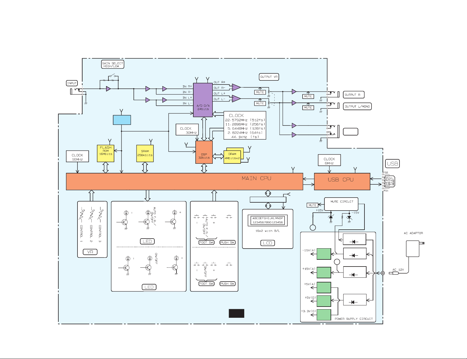
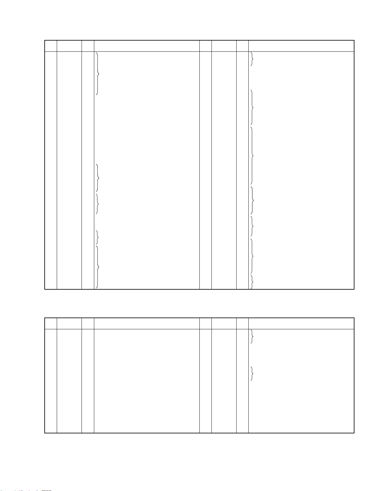
• YSS910-V (XV988B00) DSP6 (Digital Signal Processor) DM: IC5
PIN
NO. NAME I/O FUNCTION PIN
NO. NAME I/O FUNCTION
1 Vdd - Power supply (3.3 V) 89 Vss - Ground
2 Vss - Ground 90 DB13 I/O
Parallel data bus
3 XI I System master clock input (60 MHz or 30 MHz) 91 DB14 I/O
4 XO O System master clock output (High or 30 MHz) 92 DB15 I/O
5 Vdd5 - Power supply (5 V) 93 DB16 I/O
6 /SYNCI I System sync. signal input 94 DB17 I/O
7 /SYNCO O System sync. signal output 95 DB18 I/O
8 Vdd5 - Power supply (5 V) 96 DB19 I/O
9 CKI I System clock input (30 MHz) 97 DB20 I/O
10 CKO O System clock output (30 MHz) 98 DB21 I/O
11 CKSEL I
System master clock select (0: 60 MHz, 1: 30 MHz)
99 DB22 I/O
12 Vss - Ground 100 Vss - Ground
13 MCKS I Serial I/O master clock input (128 x Fs) 101 Vdd - Power supply (3.3 V)
14 /SSYNC I Serial I/O Sync. signal output 102 DB23 I/O
Parallel data bus
15 /IC I Initial clear (RESET) 103 DB24 I/O
16 /TEST I Test mode setting (0: Test, 1: Normal) 104 DB25 I/O
17 BTYP I Data bus type select (0: 8 bit, 1: 16 bit) 105 DB26 I/O
18 /IRQ O IRQ output 106 DB27 I/O
19 TRIG I/O Trigger signal input/output 107 DB28 I/O
20 Vdd5 - Power supply (5 V) 108 DB29 I/O
21 Vss - Ground 109 DB30 I/O
22 /CS I Chip select signal input 110 DB31 I/O
23 /WR I Write signal input 111
TIMO/DBOB
I/O
Timing signal output/ Parallel data bus output control input
24 /RD I Read signal input 112 Vss - Ground
25 CA7 I
Address bus of internal register
113 Vdd5 - Power supply (5 V)
26 CA6 I 114 DA00 I/O
Memory data bus
27 CA5 I 115 DA01 I/O
28 CA4 I 116 DA02 I/O
29 CA3 I 117 DA03 I/O
30 CA2 I 118 DA04 I/O
31 CA1 I 119 DA05 I/O
32 Vss - Ground 120 DA06 I/O
33 Vdd - Power supply (3.3 V) 121 DA07 I/O
34 CD15 I/O
Data bus of internal register
122 Vss - Ground
35 CD14 I/O 123 DA08 I/O
Memory data bus
36 CD13 I/O 124 DA09 I/O
37 CD12 I/O 125 DA10 I/O
38 CD11 I/O 126 DA11 I/O
39 CD10 I/O 127 DA12 I/O
40 CD09 I/O 128 DA13 I/O
41 CD08 I/O 129 DA14 I/O
42 CD07 I/O 130 DA15 I/O
43 CD06 I/O 131 Vss - Ground
44 Vss - Ground 132 Vdd - Power supply (3.3 V)
45 Vdd - Power supply (3.3 V) 133 (n.c) - Not used
46 Vdd5 - Power supply (5 V) 134 Vdd5 - Power supply (5 V)
47 CD05 I/O
Data bus of internal register
135 DA16 I/O
Memory data bus
48 CD04 I/O 136 DA17 I/O
49 CD03 I/O 137 DA18 I/O
50 CD02 I/O 138 DA19 I/O
51 CD01 I/O 139 DA20 I/O
52 CD00 I/O 140 DA21 I/O
53 /WAIT O WAIT output 141 DA22 I/O
54 Vss - Ground 142 DA23 I/O
55 SI0 I
Serial data input
143 Vss - Ground
56 SI1 I 144 DA24 I/O
Memory data bus
57 SI2 I 145 DA25 I/O
58 SI3 I 146 DA26 I/O
59 SI4 I 147 DA27 I/O
60 SI5 I 148 DA28 I/O
61 SI6 I 149 DA29 I/O
62 SI7 I 150 DA30 I/O
63 Vss - Ground 151 DA31 I/O
64 Vdd5 - Power supply (5 V) 152 Vdd5 - Power supply (5 V)
65 SO0 O
Serial data output
153 Vss - Ground
66 SO1 O 154 A00 O
Memory address (SRAM, PSRAM, DRAM)
67 SO2 O 155 A01 O
68 SO3 O 156 A02 O
69 SO4 O 157 A03 O
70 SO5 O 158 A04 O
71 SO6 O 159 A05 O
72 SO7 O 160 A06 O
73 Vss - Ground 161 A07 O
74 DB00 I/O
Parallel data bus
162 A08 O
75 DB01 I/O 163 A09 O
76 DB02 I/O 164 Vss - Ground
77 DB03 I/O 165 Vdd - Power supply (3.3 V)
78 DB04 I/O 166 A10 O Memory address (SRAM, PSRAM, DRAM)
79 DB05 I/O 167 A11 O
80 DB06 I/O 168 A12 O
Memory address (SRAM, PSRAM)
81 DB07 I/O 169 A13 O
82 DB08 I/O 170 A14 O
83 DB09 I/O 171 A15/RAS O Memory address (SRAM, PSRAM), /RAS (DRAM)
84 DB10 I/O 172 A16/CAS O Memory address (SRAM, PSRAM), /CAS (DRAM)
85 DB11 I/O 173 A17/CE O Memory address (SRAM), /CE (PSRAM)
86 DB12 I/O 174 /WE O Memory write enable signal
87 Vdd5 - Power supply (5 V) 175 /OE O Memory output enable signal
88 Vdd - Power supply (3.3 V) 176 Vdd5 - Power supply (5 V)

UB99A/UB99B/UB99MK2
11
■IC BLOCK DIAGRAM(ICブロック図)
• SN74LVU04APWR(X3936A00)
Hex Inverter
DM: IC107
• SN74LV245APWR(X3693A00)
Octal 3-State Bus Transceiver
DM: IC8,9
• SN74LV4040APWR(X3935A00)
12-Bit Asynchronous Binary Counter
DM: IC110
1
2
3
4
5
6
7
1A
1Y
2A
2Y
3A
3Y
Vss
14
13
12
11
10
9
8
Vcc
6A
6Y
5A
5Y
4A
4Y
1
2
3
4
5
6
7
20
19
18
17
16
15
14
Vcc
OE
B1
B2
B3
B4
B5
B6
B7
B8
8
9
10
12
11
GND
A8
A7
A6
A5
A4
A3
A2
A1
DIR
13
• NJM072M(XC458A00)
• TL072CPSR(XV423A00)
Dual Operational Amplifier
DM: IC101
• NJM5532M(X4980A00)
Dual Operational Amplifier
DM: IC102,103,105,106
• NJM4556AM(X5049A00)
Dual Operational Amplifier
DM: IC114
1
2
3
4
5
6
7
QL
QF
QE
QG
QD
QC
QB
GND
VCC
QK
QJ
QH
QI
CLR
CLK
QA
16
14
13
12
11
10
89
15
R
T
R
T
R
T
R
T
R
T
R
T
R
T
R
T
R
T
R
T
R
T
R
T
3
2 4 13 12 14 15 1
11
10
CLR
CLK
QAQDQE
QHQKQL
QFQGQIQJ
79
QB
65
QC
Output A
Inverting
Input A
Non-Inverting
Input A
-DC Voltage
Supply
+DC Voltage
Supply
Output B
Inverting
Input B
Non-Inverting
Input B
1
2
3
4
8
7
6
5
-+
-+
-V
1
2
3
4
8
7
6
5
A OUT
A+IN
V+
B OUT
B+IN
A IN
V
B IN
1
2
3
4
8
7
6
5
A OUT
A+IN
V+
B OUT
B+IN
A IN
V
B IN

UB99A/UB99B/UB99MK2
14
■INSPECTIONS / FACTORY SET
1. Preparation
1-1. Measuring instrument:
Oscillator, Distortion meter, Level meter
1-2. Jig:
USB cable, P.C (Personal computer)
1-3. Connections of terminals:
2. Measurement Conditions
• Unless otherwise specified, input signals are of
sinusoidal waves and the frequency is 1 kHz.
• Before turning on power, set knobs of Control VR1,
Control VR2 and Control VR3 at positions near their
respective center.
• Set VOLUME VR to maximum and INPUT LEVEL
SW to LOW.
• Make sure that the input impedance of the
measuring instrument is 1 MΩor greater.
• Install USB-MIDI driver on the P.C. Get the driver
from the Yamaha web site.
3. Method of Inspection
3-1. How to get TEST MODE
3-1-1. When turning on power while pushing [–] SW and
[+] SW, you will get TEST MODE. (This unit has no
power switch. Power is turned on by connecting the
AC adaptor.)
3-1-2. Proceed with inspection according to the instruction
in the display.
Make sure that the back light LED of LCD is lit.
3-2. DSP & DRAM & AD/DA Check
3-2-1. Push [ON/OFF] or [AUTO F.R./ON/OFF] SW. The
following display appears.
Make sure that a signal wave is outputted.
3-2-2. Check that the input and output values shown below
are satisfied.
After checking, set the INPUT LEVEL SW to LOW.
INPUT Monaural Input 1/4 inch Plug (Signal Input)
OUT L/
MONO Monaural Output 1/4 inch Plug (R
L
47 KΩ)
OUT R Monaural Output 1/4 inch Plug (R
L
47 kΩ)
PHONES Stereo Output 1/7 inch Plug (R
L
33 Ω)
AC IN AC ADAPTOR (AC-10)
USB USB Cable →P.C.
INPUT
LEVEL HIGH (+10 dB) / LOW (0 dB)
UB99@P.CHEK@V1.0@
PUSH@[ON/OFF]@SW
UB99@DSP&DRAM@
PUSH@[ON/OFF]@SW
INPUT LEVEL
SW setting
Item
Input terminal,
Conditions
Output terminal,
Specifications
LOW
1: Input
sensitivity
INPUT
-4.5 dBm (1 KHz)
OUT L/MONO
0 dBm ±3 dB
2: ditto INPUT
-4.5 dBm (10 KHz)
OUT L/MONO
0 dBm ±3 dB
3: ditto INPUT
-4.5 dBm (100 KHz)
OUT L/MONO
0 dBm ±3 dB
4: ditto INPUT
-22.5 dBm (100 Hz)
OUT R
0 dBm ±3 dB
5: ditto INPUT
-22.5 dBm (10 KHz)
OUT R
0 dBm ±3 dB
6: ditto INPUT
-22.5 dBm (1 KHz)
OUT R
0 dBm ±3 dB
7: ditto INPUT
-13.5 dBm (1 KHz)
PHONES R
0 dBm ±3 dB
8: ditto INPUT
-13.5 dBm (10 KHz)
PHONES R
0 dBm ±3 dB
9: ditto INPUT
-12.5 dBm (100 Hz)
PHONES R
0 dBm ±3 dB
10: ditto INPUT
+5.5 dBm (100 Hz)
PHONES L
0 dBm ±3 dB
11: ditto INPUT
+4.5 dBm (10 kHz)
PHONES L
0 dBm ±3 dB
12: ditto INPUT
+4.5 dBm (1 kHz)
PHONES L
0 dBm ±3 dB
HIGH
13: ditto INPUT
-15 dBm (1 KHz)
OUT L/MONO
0 dBm ±3 dB
14: Noise level INPUT
Pull Out Plug
OUT L/MONO
-44 dBm or less
15: ditto INPUT OUT R
-44 dBm or less
16: ditto INPUT PHONES L
-52 dBm or less
17: ditto INPUT PHONES R
-52 dBm or less
18: Distortion
factor
INPUT
-12 dBm (1 KHz)
Push Insert Plug
OUT R
0.5% or less
19: ditto INPUT
+6 dBm (1 KHz)
OUT L/MONO
0.5% or less
20: ditto INPUT
+8 dBm (1 KHz)
PHONES L
0.5% or less
21: ditto INPUT
-10 dBm (1 KHz)
PHONES R
0.5% or less
0 dBm=0.775 V

UB99A/UB99B/UB99MK2
15
3-3. SRAM Check
3-3-1. Push [ON/OFF] or [AUTO F.R./ON/OFF] SW. The
following display appears.
In a short time, the display is changed as follows.
Check for the OK sign in the display.
3-4. FLASH ROM Check
3-4-1. Push [ON/OFF] or [AUTO F.R./ON/OFF] SW. The
following display appears.
In a short time, the display is changed as follows.
Check for the OK sign in the display.
3-5. SW&LED Check
3-5-1. Push [ON/OFF] or [AUTO F.R./ON/OFF] SW. The
following display appears.
Check for the OK sign in the display.
3-5-2. Push [-] SW. The following display appears.
and LED (-) will be turned on.
3-5-3. Push [ON/OFF] or [AUTO F.R./ON/OFF] SW. The
following display appears.
Then, LED [ON/OFF] or [AUTO F.R./ON/OFF] will
be turned on.
3-5-4. Push [+] SW. The following display appears.
Then, LED (+) will be turned on.
3-5-5. Push [STORE/EXIT] SW. The following display
appears.
Then, three LEDs, LED (-), LED [ON/OFF] or
[AUTO F.R./ON/OFF], and LED (+) will be turned
on.
Check for the OK sign in the display.
3-6. VR Check
3-6-1. Push [ON/OFF] or [AUTO F.R./ON/OFF] SW. The
following display appears.
The LEDs will be turned off.
“**” represents each of VR values, and “[]” shows
the position of the VR to be inspected.
Before checking, set each VR to center.
3-6-2. Turn VR1 (Control 1) fully clockwise. The following
display appears.
3-6-3. Turn VR1 (Control 1) fully counterclockwise. The
following display appears.
UB99@SRAM@CHECK@
NOW@WRITE@&@READ
UB99@SRAM@CHECK@
OK@PUSH[ONOFF]SW
UB99@FLASH@ROM
NOW@WRITE@&@READ
UB99@FLASH@ROM
OK@PUSH[ONOFF]SW
UB99@SW&LED@CHEK
PUSH@[-]@SWITCH
UB99@SW&LED@CHEK
PUSH@[ON/OFF]@SW
UB99@SW&LED@CHEK
PUSH@[+]@SWITCH
UB99@SW&LED@CHEK
PUSH@[STORE]@SW
UB99@SW&LED@CHEK
PUSH@[ON/OFF]@SW
UB99@VOL1@CHECK
MAX@[**]@**@@**@@
VR1 VR2 VR3
UB99@VOL1@CHECK
MIN@[ff]@@**@@**@
UB99@VOL1@CHECK
UP@@[00]@**@@**@@

UB99A/UB99B/UB99MK2
16
3-6-4. Turn VR1 (Control 1) to center. The following
display appears.
3-6-5. Turn VR2 (Control 2) fully clockwise. The following
display appears.
3-6-6. Turn VR2 (Control 2) fully counterclockwise. The
following display appears.
3-6-7. Turn VR2 (Control 2) to center. The following
display appears.
3-6-8. Turn VR3 (Control 3) fully clockwise. The following
display appears.
3-6-9. Turn VR3 (Control 3) fully counterclockwise. The
following display appears.
3-6-10. Turn VR3 (Control 3) to center. The following
display appears.
Check for the OK sign in the display.
3-7. USB Check
3-7-1. Push [ON/OFF] or [AUTO F.R./ON/OFF] SW. The
following display appears.
3-7-2. Connect with PC by USB cable. The following
display appears.
3-7-3. Remove the USB cable. The following display
appears.
Check for the OK sign in the display.
3-8. LCD Check
3-8-1. Push [ON/OFF] or [AUTO F.R./ON/OFF] SW. The
following display appears.
3-8-2. Push [ON/OFF] or [AUTO F.R./ON/OFF] SW. The
following display appears.
All the LEDs will be turned on.
3-9. END
3-9-1. Push [ON/OFF] or [AUTO F.R./ON/OFF] SW. The
following display appears.
Turn off power, and the inspection is now
completed.
Finally, perform “4. Factory Set” as follows.
UB99@VOL2@CHECK
MAX@@**@[**]@**@@
UB99@VOL2@CHECK
MIN@@**@[ff]@**@@
UB99@VOL2@CHECK
UP@@@**@[00]@**@@
UB99@VOL3@CHECK
MAX@@**@@**@[**]
UB99@VOL3@CHECK
MIN@@**@@**@[ff]
UB99@VOL3@CHECK
UP@@@**@@**@[00]
UB99@VOL3@CHECK
OK@PUSH[ONOFF]SW
UB99@USB@CHECK
V10103@CNECT@USB
UB99@USB@CHECK
DISCONNECT@CABLE
UB99@USB@CHECK
OK@PUSH[ONOFF]SW
UB99@LCD@CHECK@@
PUSH@[ON/OFF]@SW
~~~~~~~~~~~~~~~~
~~~~~~~~~~~~~~~~
UB99@DIAG@ALL@OK
PLEASE@POWER@OFF

UB99A/UB99B/UB99MK2
17
4. Factory Set
4-1. Turn on power while pushing [ON/OFF] or [AUTO
F.R./ON/OFF] SW and [STORE/EXIT] SW. The
following display appears.
4-2. Push [+] SW. The following display appears.
4-3. Push [STORE/EXIT] SW. The following display
appears.
Then, the display is changed as follows.
The Factory Set is completed.
Then, “5.Opening” display will appear and operation
returns to a normal condition.
4-4. At the time of cancellation, the following display
appears.
5. Opening
• In this mode, the following display appears.
Then, the display is changed as follows.
Finally, the display is changed as follows.
Turn off power and finish the procedure.
Turn off power, and the inspection is now completed. If you
reset UB99A/ UB99B/ UB99MK2 to the factory default setting,
all of the batch contents you saved are erased. Take notes of
the settings, or save the settings on your computer, if
necessary (See page 22).
@@FACTORY@@SET
@NO:[-]@YES:[+]
@@FACTORY@@SET
SURE?PUSH[STORE]
@@FACTORY@@SET
NOW@FACTORY@SET!
@@FACTORY@@SET
@@@COMPLETE!!@@@
@@FACTORY@@SET
@@@CANCELLED!@@@
@@@MAGICSTOMP@@@
@@@@@V2.00
(This picture shows an example of UB99MK2.)
* “V2.00” indicates the version of the firmware. This
number is subject to change due to the specification
change.
@\
WAIT@A@MOMENT...
U01)HeavyHiGain
@@GAIN@MSTR@TONE
(This picture shows an example of UB99MK2.)

UB99A/UB99B/UB99MK2
18
■検査 / ファクトリーセット
1. 準備
1-1. 測定器:
発振器、 歪率計、 レベル計
1-2. 治具:
USB ケーブル、 P.C. (パー ソ ナル コ ン ピ ュー タ )
1-3. 各端子の接続:
2. 測定基準
•特に規定の無い場合の入力信号は正弦波、 周波数は
1KHz と し ます。
•電源を投入す る前に、 Control VR1、 Control VR2、
Control VR3 のツマ ミ を セン ター 付近に設定 し ます。
•VOLUME VR は最大、INPUT LEVEL SW は LOW に設
定します。
•測定器の入力 イ ン ピーダ ン スは1MΩ以上であ る こ と
を確認し ます。
•
P.C. に USB-MIDI ド ラ イ バーを イ ン ス ト ールし ます。 ド
ライバーはヤマハウェブサイトから入手してください。
3. 検査方法
3-1. TESTMODEの入り方
3-1-1. [ - ] SW、 [ + ] SW を押 し なが ら 電源を投入する と
TEST MODE に入 り ます。(本体に電源ス イ ッ チはあ
り ません。 AC ア ダプ タ ーを接続す る と 電源が投入
されます。)
表示に し たがい検査を進め ます。
必ず LCD バ ッ ク ラ イ ト (LED) が点灯 し てい る こ と
を確認し て く ださい。
3-2. DSP&DRAM&AD/DACheck
3-2-1. [ON/OFF] ま たは [AUTO F.R./ON/OFF] SW を押 し
ます。
と 表示 さ れ、信号波形が出力 さ れる の を確認 し ます。
3-2-2. 入出力の値が下表 を満た し て い る こ と を確認 し て
ください。
確認後、 INPUT LEVEL SW を LOW に設定 し て く だ
さい。
INPUT モ ノ ラル入力 (Signal Input)
OUT L/
MONO モノラル出力 (R
L
47 KΩ)
OUT R モ ノ ラル出力 (R
L
47 KΩ)
PHONES ス テ レ オ出力 (R
L
33Ω)
AC IN AC アダプ ター (AC-10)
USB USB ケーブル → P.C.
INPUT
LEVEL HIGH (+10dB) / LOW (0dB)
UB99@P.CHEK@V1.0@
PUSH@[ON/OFF]@SW
UB99@DSP&DRAM@
PUSH@[ON/OFF]@SW
INPUTLEVEL
SW 設定
項目 入力端子、条件 出力端子、
規格値
LOW
1: 入力感度 INPUT
-4.5 dBm (1 KHz)
OUT L/MONO
0 dBm ± 3 dB
2: 同上 INPUT
-4.5 dBm (10 KHz)
OUT L/MONO
0 dBm ± 3 dB
3: 同上 INPUT
-4.5 dBm (100 Hz)
OUT L/MONO
0 dBm ± 3 dB
4: 同上 INPUT
-22.5 dBm (100 Hz)
OUT R
0 dBm ± 3 dB
5: 同上
INPUT
-22.5 dBm (10
KHz)
OUT R
0 dBm ± 3 dB
6: 同上 INPUT
-22.5 dBm (1 KHz)
OUT R
0 dBm ± 3 dB
7: 同上 INPUT
-13.5 dBm (1 KHz)
PHONES R
0 dBm ± 3 dB
8: 同上
INPUT
-13.5 dBm (10
KHz)
PHONES R
0 dBm ± 3 dB
9: 同上 INPUT
-12.5 dBm (100 Hz)
PHONES R
0 dBm ± 3 dB
10: 同上 INPUT
+5.5 dBm (100 Hz)
PHONES L
0 dBm ± 3 dB
11: 同上 INPUT
+4.5 dBm (10 kHz)
PHONES L
0 dBm ± 3 dB
12: 同上 INPUT
+4.5 dBm (1 kHz)
PHONES L
0 dBm ± 3 dB
HIGH
13: 同上 INPUT
-15 dBm (1 KHz)
OUT L/MONO
0 dBm ± 3 dB
14: ノイズ
レベル
INPUT
入力プ ラ グ を 抜き
ます
OUT L/MONO
-44 dBm 以下
15: 同上 INPUT OUT R
-44 dBm 以下
16: 同上 INPUT PHONES L
-52 dBm 以下
17: 同上 INPUT PHONES R
-52 dBm 以下
18: 歪率
INPUT
-12 dBm (1 KHz)
入力プ ラ グ を 差し
ます
OUT R
0.5% 以下
19: 同上 INPUT
+6 dBm (1 KHz)
OUT L/MONO
0.5% 以下
20: 同上 INPUT
+8 dBm (1 KHz)
PHONES L
0.5% 以下
21: 同上 INPUT
-10 dBm (1 KHz)
PHONES R
0.5% 以下
0dBm=0.775V

UB99A/UB99B/UB99MK2
19
3-3. SRAMCheck
3-3-1. [ON/OFF] ま たは [AUTO F.R./ON/OFF] SW を押し
ます。
と表示し、 しばら くすると
と 表示 され ます。 OK 表示を確認 し て く だ さ い。
3-4. FLASHROMCheck
3-4-1. [ON/OFF] ま たは [AUTO F.R./ON/OFF] SW を押し
ます。
と表示し、 しばら くすると
と 表示 さ れます。 OK 表示を確認 し て く だ さ い。
3-5. SW&LEDCheck
3-5-1. [ON/OFF] ま たは [AUTO F.R./ON/OFF] SW を押し
ます。
と表示されます。
3-5-2. [ - ] SW を押し ます。
と表示されLED (-)が点灯します。
3-5-3. [ON/OFF] ま たは [AUTO F.R./ON/OFF] SW を押し
ます。
と 表示 さ れ LED (ON/OFF ま たは AUTO F.R./ON/
OFF) が点灯し ます。
3-5-4. [+] SW を押し ます。
と 表示 さ れ LED (+) が点灯 し ます。
3-5-5. [STORE/EXIT] SW を押 し ます。
と 表示され LED ( - ) 、 LED (ON/OFF ま たは AUTO
F.R./ON/OFF)、 LED (+) が 3 個点灯し ます。
OK 表示を確認 し て く だ さ い。
3-6. VRCheck
3-6-1. [ON/OFF] ま たは [AUTO F.R./ON/OFF] SW を押 し
ます。
と 表示 さ れ ます。 LED は消灯 し ます。
**はそれぞれのVRの値を表示し ます。[ ]が検査す
る VR の位置を示し ます。
検査の前に、 必ず各 VR をセ ン タ ー付近に設定 し て
ください。
3-6-2. VR1 (Control 1) を右にいっぱい まで回し ます。
と表示されます。
3-6-3. VR1 (Control 1) を左にいっぱい まで回し ます。
と表示されます。
UB99@SRAM@CHECK@
NOW@WRITE@&@READ
UB99@SRAM@CHECK@
OK@PUSH[ONOFF]SW
UB99@FLASH@ROM
NOW@WRITE@&@READ
UB99@FLASH@ROM
OK@PUSH[ONOFF]SW
UB99@SW&LED@CHEK
PUSH@[-]@SWITCH
UB99@SW&LED@CHEK
PUSH@[ON/OFF]@SW
UB99@SW&LED@CHEK
PUSH@[+]@SWITCH
UB99@SW&LED@CHEK
PUSH@[STORE]@SW
UB99@SW&LED@CHEK
PUSH@[ON/OFF]@SW
UB99@VOL1@CHECK
MAX@[**]@**@@**@@
VR1 VR2 VR3
UB99@VOL1@CHECK
MIN@[ff]@@**@@**@
UB99@VOL1@CHECK
UP@@[00]@**@@**@@

UB99A/UB99B/UB99MK2
20
3-6-4. VR1 (Control 1) をセ ン ター付近ま で回し ます。
と表示されます。
3-6-5. VR2 (Control 2) を右にいっぱいま で回 し ます。
と表示されます。
3-6-6. VR2 (Control 2) を左にいっぱいま で回 し ます。
と表示されます。
3-6-7. VR2 (Control 2) をセ ン ター付近ま で回し ます。
と表示されます。
3-6-8. VR3 (Control 3) を右にいっぱい まで回 し ます。
と表示されます。
3-6-9. VR3 (Control 3) を左にいっぱいま で回 し ます。
と表示されます。
3-6-10. VR3 (Control 3) をセ ン ター付近ま で回し ます。
と 表示 さ れ ます。 OK 表示 を確認 し て く だ さ い。
3-7. USBCheck
3-7-1. [ON/OFF] ま たは [AUTO F.R./ON/OFF] SW を押し
ます。
と表示されます。
3-7-2. USB Cable で P.C. と 接続 し ます。
と表示されます。
3-7-3. USB Cable を抜き ます。
と 表示 さ れます。 OK 表示を確認 し て く だ さ い。
3-8. LCDCheck
3-8-1. [ON/OFF] ま たは [AUTO F.R./ON/OFF] SW を押し
ます。
と表示されます。
3-8-2. [ON/OFF] ま たは [AUTO F.R./ON/OFF] SW を押し
ます。
と 全点灯 さ れます。
3-9. END
3-9-1. [ON/OFF] ま たは [AUTO F.R./ON/OFF] SW を押し
ます。
と表示されます。
電源を OFF に し ます。
こ れで検査は終了 と な り ます。
最後に 4. フ ァ ク ト リ ーセ ッ ト を行ないます。
UB99@VOL2@CHECK
MAX@@**@[**]@**@@
UB99@VOL2@CHECK
MIN@@**@[ff]@**@@
UB99@VOL2@CHECK
UP@@@**@[00]@**@@
UB99@VOL3@CHECK
MAX@@**@@**@[**]
UB99@VOL3@CHECK
MIN@@**@@**@[ff]
UB99@VOL3@CHECK
UP@@@**@@**@[00]
UB99@VOL3@CHECK
OK@PUSH[ONOFF]SW
UB99@USB@CHECK
V10103@CNECT@USB
UB99@USB@CHECK
DISCONNECT@CABLE
UB99@USB@CHECK
OK@PUSH[ONOFF]SW
UB99@LCD@CHECK@@
PUSH@[ON/OFF]@SW
~~~~~~~~~~~~~~~~
~~~~~~~~~~~~~~~~
UB99@DIAG@ALL@OK
PLEASE@POWER@OFF
This manual suits for next models
2
Table of contents
Other Yamaha Recording Equipment manuals

Yamaha
Yamaha SFGII User manual

Yamaha
Yamaha TX816 Quick start guide

Yamaha
Yamaha MU1000 User manual

Yamaha
Yamaha TX-216 User manual

Yamaha
Yamaha S Rev1 User manual

Yamaha
Yamaha TQ5 User manual

Yamaha
Yamaha TQ5 User manual

Yamaha
Yamaha DR100 User manual

Yamaha
Yamaha MU10 User manual

Yamaha
Yamaha QX-7 User manual

Yamaha
Yamaha MY8-SDI-ED User manual

Yamaha
Yamaha POCKETRAK CX User manual

Yamaha
Yamaha TX-216 User manual

Yamaha
Yamaha MDF1 User manual

Yamaha
Yamaha YPC-1 User manual

Yamaha
Yamaha HY144-D-SRC User manual

Yamaha
Yamaha TX-802 User manual

Yamaha
Yamaha REV7 User manual

Yamaha
Yamaha HY256-TL-SMF User manual

Yamaha
Yamaha REV500 User manual