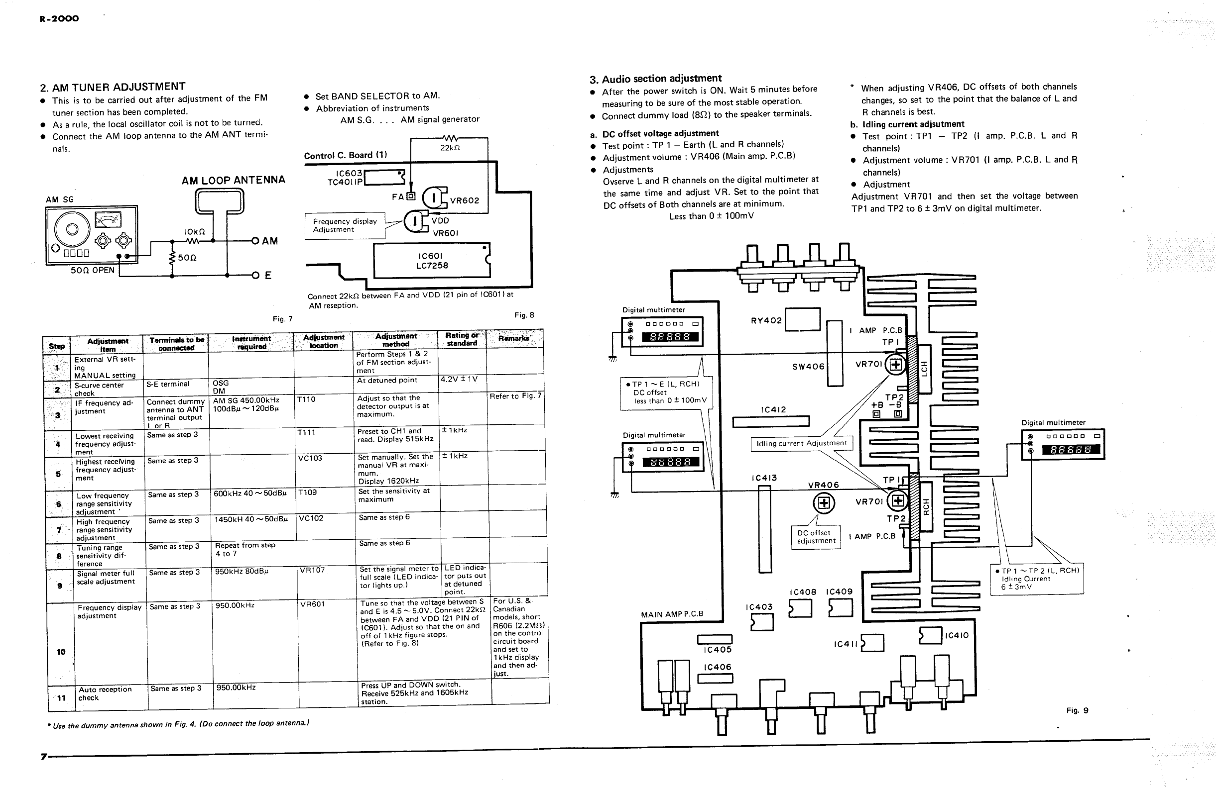
manuals.online logo
Brands
  1. Home
  2. •
  3. Brands
  4. •
  5. Yamaha
  6. •
  7. Stereo Receiver
  8. •
  9. Yamaha R-2000 User manual

Yamaha R-2000 User manual

STEREO RECEIVER
SERVI CE MANUAL
FRONT PANEL
~~'
ij::
~:'~ : " : , : " : ~'-
~ o ~~F-
"~~~"::- ~~'.~
..J.
. . ' ~ ~.. -. ., -. """,
0 POWER SWITCH
f) RX MODE INDICATOR
..
TUNING LEVEL INDICATOR
e FM STEREO INDICATOR
. STATION LOCK INDICATOR
41) SIGNAL QUALITY INDICATOR
. AM/FM INDICATOR
fI) DIGITAL FREQUENCY READOUT
'I) AUIO PHONO SWITCH
. INPUT SELECTOR BUTTONS
. PRESET STATION BUTTONS
. VOLUME CONTROL
. TUNING LEVEL BUTTONS
MEMORY BUTTON
. TUNING BUTTON
. BAND SELECT BUTTONS
. PHONES JACKS
. SPEAKERS SELECTOR
. SUBSONIC FILTER SWITCH
. HIGH FILTER SWITCH
. BASS CONTROL
. PRESENCE CONTROL
. TREBLE CONTROL
. SPATIAL EXPANDER CONTROL
. PRE-MAIN COUPLER SWITCH
..
REC OUT SELECTOR
. PHONO SELECTOR
. BALANCE CONTROL
. LOUDNESS CONTROL
. MODE SWITCH
-- FM MUTING SWITCH
..
RX MODE SWITCH
_CONTENTS
REAR PANEL.........................
INTERNAL VIEW
......................
DISASSEMBLY PROCEDURES. . . . .
. . . . . . . .
MEASUREMENT AND ADJUSTMENT.
. . . . . . .
SPECIFICATION....................... 8
BLOCK DIAGRAM ..................... 9
WIRING DIAGRAM .....................
SCHEMATIC DIAGRAM..................
SINCE 188i
. V AMAHA
I 004433 I NIPPON GAKKI CO. LTO HAMAMAT5U. JAPAN
2000
REAR PANEL
~ U. A. & CANADIAN MODELS
~ GENERAL MODEL
~.:_.
::;o
:..:... '-""--""--
_..._...-. i
""" .., '" '" .
~~~o
W IT) 0 0
. (J)(!)(!)(!)(!)(8J.
~ BRITISH & AUSTRALIAN MODELS
~ NORTH EUROPEAN MODEL
0 GROUND TERMINAL
f) AUX I NPUT JACKS
.TAPE 1 PB/REC JACKS
GTAPE 2 PB/REC JACKS
.SPEAKERS TERMINAL
. AC OUTLETS
. PHONO I NPUT JACKS
fI) FM ANTENNA TERMINAL (75m
'I) FM ANTENNA TERMINAL (300n)
.AM GROUND TERMINAL
cii;~;';oo
~~'(!)
(!)tJ)(IH!)rn !\'
~- ~...- .. --. ..
0. --..
(j)'
(!) (!jd) d)' ,
(!)~ (!)
~ m
. .. - . . -... ... --.
(j)~d) .(j)~(!) d)~ '
(!) ~ (!)~ (!)
.AM ANTENNA TERMINAL
. PRE OUT/MAIN IN JACKS
. POWER CORD
. VOLTAGE SELECTOR
_INTERNAL VIEW
~ TOP VIEW
_DISASSEMBLY PROCEDURES
1. Top Cover Removal
Remove the screws CD and CV in photo 1 from both
right and left sides, then remove the top cover,
Photo 1
K-:'UJUU
0 POWER TRANSFORMER GA6465 (U)
GA6466 (C)
GA6468 (R)
GA6467 (G)
GA6469 (A. B)
f) ELECTROLYTIC CAPACITOR CIRCUIT BOARD
(Power supply)
.. MAIN CIRCUIT BOARD (1
G I AMP CIRCUIT BOARD
. AM LOOP ANTENNA
.. TUNER CIRCUIT BOARD
. FRONT END PACK PK101
fI) MAIN CIRCUIT BOARD (3) (Pin Jacks)
. CONTROL CIRCUIT BOARD (6) (Phones Jacks)
.CONTROL CIRCUIT BOARO (2)
.CONTROLCIRCUIT BOARD (4)
. CONTROL CIRCUIT BOARD (1)
. MAIN CIRCUIT BOARD (4)
. MAIN CIRCUIT BOARD (2)
. CONTROL CIRCUIT BOARD (3)
. CONTROL CIRCUIT BOARD (5)
2. Bottom Cover Removal
Remove the screws CD to (jj in photo 2 and then
remove the bottom cover.
'"' . -
'It 7
. mn1l1HIIIII~0
. . 0111111111
'13- .
111111111111111111111111
111111111111111111111111
111111111111111111111111
Photo 2
K-:.I:UUU
3. Front Panel Removal
a. Loosen the set screws of SPEAKERS, REC OUT
PRESENCE and PHONO knobs with a 1.5 mm hex-
agon wrench, then pull out each knob.
b. Remove the screws T to ':1) in photo 3 and remove
the front panel.
* Remove the screws ':1: to W in photo 2 when the
front panel is removed.
Photo 3
4. Main C. Board (2) Removal
a. Detach the connectors and PHONO, TUNER indica-
tor lamps which are attached to the Main C. Board.
Refer to Fig. 1.
How to connect the wires to the jumper socket.
Fig. 1
b. Remove the screws CD and CID in photo 4 and then
remove the Main C. Board (2).
;~ i ~/3
:_...:~ ;~:
Y-.
~-:\r
':-:
'j r
. '
~r.
;j:f: "" ;(0 .
;J,
:-
r)
~...
'r.
..
1E) "!r)('~ ni!" )
- ~ .
('-' u
: , ' -. . . . ' ~
';0 ,:
-. -. -'
Photo 4
5. Main C. Board (4) Removal
a. Remove the plastic rivets (!) and CID in photo 4 and
then remove the Main C, Board (4).
b. Detach the lead wires which are attached to the Main
C, Board (4).
6. Control C. Board (3) Removal
a, Remove the Main C. Board, (Refer to step 4 and 5.
b. Remove the plastic rivets (!) to CID in photo 4 and
then remove the Control C. Board (3).
c. Detach the lead wires which are attached to the
Control C. Board (3) .
7. Control C. Board (5) Removal
a. Detach the lead wires which are attached to the
Control C. Board (5) .
b, Remove the nut CID in photo 4 and remove the
Control C. Board (5) .
8. Main C. Board (3) Removal
a. Remove the connectors and Remoto Rotary Switch,
* How to detach and attach the remoto rotary switch.
When the knob is rotated fully clockwise.
R,mo," '0,,"'" ~;tth,
Switch
-=-==1 c:: :Lf1--
::.. ..:-.:-
I '
C. board
Check that the switch can be operated
precisely after attaching it.
Fig.
b. Detach the lead wires which are attached to the Main
C. Board (3J .
c. Remove the screws CID in photo 3 and CD to (!) in
photo 5 and then remove the Main C, Board (3J.
' " , ' . ". ," ' ' ' . ,;. - : . ~ ' : .. . ::. .
Photo 5
9. Tuner C. Board Removal
a. Detach the connector, remote rotary switch and lead
wires which are attached to the Tuner C. Board,
b. Remove the nuts to (jj in photo 4 and screws (jj
to ~ in photo 4 and then remove the sub schassis
unit toward yourself,
c. Remove the screws
(j)
to CID in photo 3 and the
screws CID to (jJ) in photo 5 and then pull out the
Tuner C. Board to the front side.
10. Control C. Board (1) Removal
a. Remove the Control C. Board (1J. (Refer to step 10,
b. Remove the plastic rivet to ~ in photo 4 and
then remove the holder unit.
c. Remove the Control C. Board from the sub schassis
unit.
d. Detach the lead wires which are connected to the
Control C. Board (1).
11. Control C. Board (3) Removal
a. Remove the Control C. Board (1 J and (4) . (Refer to
step Q9) and (jJ) ,
b. Remove the plastic rivet to ~ in photo 4 and
remove the Control C. Board (3) .
c. Detach the lead wires which are connected to the
Control C. Board (3J .
12. I AMP. C. Board Removal
a, Detach the lead wires which are connected to the I
AMP. C. Board.
b. Remove the screws (jj) and (jJ) in photo 3 and then
remove the heat sink,
c. Remove the screws CD to
(j)
in photo 6 and then
remove the I AMP. C. Board. (L and R channel are
common.
13. Main C. Board Removal
a. Detach the lead wires, connectors and remote rotary
switch which are connected to each C. Boards.
b. Remove the sub schassis unit toward yourself to
according to step 9 (b).
c. Remove the heat sink according to step 12 (b).
d. Remove the screws (jj to (jj) in photo 3 and the
screws (jj) and (jJ) in photo 5 and then remove the
Main C. Board gently.
14. Electrolytic Capacitor C. Board Removal
a, Remove the screws ifi) to in photo 3 and then
remove the Electrolytic Capacitor C, Board.
b. Detach the lead wires which are connected to the
Electrolytic Capacitor C. Board.
15. Power Transformer Removal
a, Detach the lead wires of the Power Transformer.
b. Remove the bottom cover according to step 2.
c. Remove the screws CD to '1) in photo 7 and then
remove the Power Transformer.
Photo 7
16. Phones Jack (Control C. Board (6) ) Removal
a. Remove the screws ~ and ~ in photo 4 and then
remove the power switch.
b. Pull out the phone jack stopper and ~ to the
war directed by allows in photo 4 and then remove
the Control C. Board (6),
c. Detach the lead wires which are connected to the
Control C, Board (6).
2000
_MEASUREMENT AND ADJUSTMENT
1. FM TUNER ADJUSTMENT
Before adjusting connect the auxial iary center meter
(JiOO036 or similar one) between Sand NVCC.
. Set the switches to the following positions.
Bandselect...,.................. FM
RXMODE ................... AUTO
TUNING LEVEL ............... HIGH
MUTING ......................
During adjustments, use a low-pass filter.
Start adjustment, after waiting 5 minutes following
power switch-on.
ADJUSTING POINTS
Tuner C, Board (1)
. Do not forget to keep the bottom cover on.
Abbreviation of Instruments
FM S.G. FM Signal generator
DM Digital multimeter
OSC. Oscilloscope
DIST. M. : Distortion meter
C. Frequency counter
ST SG : Stereo Signal generator
VRIOI FM Stereo
Distortion
Adjustment
AM Sensitivity
Adjustment
(Low Frequency
Range)
FM Stereo
Distortion
Adjustment
I F Frequency
Adjustment
FM FRONT END
FRONT END
1FT
6g~69P
PLL Input Phase
Adjustment
VRJO8
!1:
UJ (\j
...J
UJ -
(J) ~
(J)
'C"O
4559
AM Sensitivity I
Adjustment
(High Frequency
Range)
rclo9
. LA2300
Fig.
0605
--f+- III"'~ IC6O3 rM Frequency
TC401lP Display Adjustment
:i:~ ~
~g~
VR6
...
; VR602
"'~ '"
CD 0 c: AM Frequency
g~8 Display
c: .
g -g ~
R606 . Adjustment
;; ~ ~ ~
J603
u~o
oo.~E IC601
LC7258
VR500
~g;2"o~
L""'J
VR603
Control C, Board (1)
Fig.
Step Adjustment Terminals to be Instrument Adjustment Adjustment Reting or Reinllrits
item connected required location method standerd
External VR sett- , Vref, E Connect VR between Tune manual-
ing (control c. board) Vref and E. Iy with this
Connect the center VR when ad-
tap of VR to MT. lusting.
(Refer to Fig. 5)
Manual set Short wire Short MA (TP) and E Set MA to L
for a moment. (Refer level once.
to Fig. 5)
S curve adjustment FM antenna OSC T102 At detuned point
terminal (300n (discriminator MUTE LOCAL
balanced ANT) FM SG/ST coil) 5 - 5.
, E terminal DIST. M OFF 0 - 5.
Tuning point sett- FM antenna FM SG 98MHz External VR Adjust VR so that the voltage be- Check that JF
ing terminal Antenna input:70dB/l tween Sand E is 4.5 - 5. MODE switch
becomes Local.
Monaural distor- FM antenna FM SG 98MHz VC101 Reduce distortion to Less than Check that JF
tion adjustment terminal Antenna input:70dB/l (trimmer) mir:imum. 60dB MODE Switch
output Monaural:1 kHz 100% 70dB) becomes Local.
modulation
OSC
DIST.
VCO FM antenna FM SG 98MHz non- VR105 :;jet to 1 ~kHZ III!hen 19kHz Check that JF
adjustment terminal output modulation forcing the set Into the :t 20Hz MODE Switch
stereo mode.
19kM, ME F .C. 1 Mn resistor (Refer to Fia. 6) (:t 10Hz) becomes Local.
PLL input phase Same as step 6 FM SG 98MHz T107 Adjust so that Land Check that JF
adjustment Antenna input:70dB/l R output are at MODE Switch
Stereo L R:1 kHz maximum. becomes Local.
100% modulation DM
Stereo distortion Same as step 6 FM SG 84MHz T101 Reduce distortion to Less than Check that JF
adjustment Antenna input:70dB/l VR101 minimum 60dB MODE Switch
Stereo L R:1 kHz VR102 70dB) becomes Local.
100% modulation Front end 1FT
OSC
DIS. M
Separation Same as step 6 Same as step 8 VR103 (L ~R) Adjust so that separa- More than Check that JF
adjustment VR104(R~L) tion is at maximum. 40dB MODE Switch
(58dB) becomes Local.
Pilot canceling Same as step b Same as step 8 T108 Observe wave forms Less than Check that JF
adjustment Pilot:9% modulation VR106 on oscilloscope and 50dB MODE Switch
adjust so that leak (-BOdB) becomes Local.
level is reduced to
minimum.
Signal meter full Same as step 6 Same as step 8 VR108 Adjust so that LED of Check that
scale adjustment Stereo L R:1 kHz signal meter is at full LED is not
100% modulation scale. out at de-
tuned point.
S curve offset same as step 3 Adjust over again from
check step 3 when S curve off-
set is not found to be with-
in specified value.
Check that IF MODE
Switch becomes AUTO,
Step Adjustment
item
Frequency display
adjustment (I F
offset)
erminals to be
connected
Same as step 4
Adjustment Rating or
method stlnderd
Tune so that the voltage between
Sand E becomes 4.5V - 5V.
Four figure display; The best point
is found when the number of tenth
figu re changes.
Five figure display; Connect 22kn
between FA and E. The best point
is found when the on and off of the
display of 1 Oak figure is stopped.
North European, British models.
(Refer to Fig. 5)
Set to the highest frequency with ex-
external VR. Adjust VR604 so that
display frequency becomes 108.
35M Hz. Next, memorize in CH1 and
read. Adjust with VR603 so that dis-
play becomes 87.35MHz.
Remarks
Instrument
required
FM SG 98MHz
Antenna input: 70dB/l
Stereo (frequency
accuracy:within
:t 5kHz)
Adjustment
location
602
Band edge check Same as step 4
(receiving frequen-
cy range check)
Same as step 13
. Connect J603 to
control C. board
and detach after
adjustment except
North European
and British models.
FM SG 98MHz
Antenna input:70dB/l
VR603
VR604
Press UP and DOWN
switch. Receive
87.5MHz and 108MHz
station.
Check that Tuning
LEVEL switch is not
stopped at HIGH when
the set is auto tuned.
Auto reception
check Same as step 4
Tuning level check I Same as step 4 FM SG 98MHz
Antenna input:20dB/l
16 .
Specified values are ones that are able to be measured with YHP4333A (except step , 7 and 14).
Step shows the circuit for easy adjustment that holds an optional frequency.
Step means the rest operation to operate manually.
External VR setting Manual setting
Short MA (TP)
and E for a moment
...,
C6O3
Td401lP FA f7)J
t VR601
\.!.b V.602
R606
IC601
LCl2"
External VR
10kn Note; North European and British
models. Connect 22kn between FA and
Eat FM reseption.
III II
I .
IC604
LCna7
VR604
:;:.
VR603
22kCl
Control C, Board (1) Fig. 5
VCO Adjustment TIO7
VRIO3 VRIO4 ~
~b=d +
~~~
ICIO3
LA3380 IMCl 19
19kHz TP
(Connect +12 with 19KM by
means of a 1Mn resistor, to
force it into the stereo mode,)
(The counter
earth line should
be grounded at a
location as close
as possible to the
test point,)
Frequency counter
DODD
0000
ICIO4D lelTIO8 19kHz:t20Hz
(Reference value
:t10Hz) Fig. 6Tuner C. Board (1) VRIO6
2000
2. AM TUNER ADJUSTMENT
This is to be carried out after adjustment of the FM
tuner section has been completed.
. As a rule , the local oscillator coil is not to be turned.
. Connect the AM loop antenna to the AM ANT termi-
nals.
AM LOOP ANTENNA
AM SG
. Set BAND SELECTOR to AM.
Abbreviation of instruments
AM S.G. . . . AM signal generator
3. Audio section adjustment
After the power switch is ON. Wait 5 minutes before
measuring to be sure of the most stable operation.
. Connect dummy load (Sn) to the speaker terminals.
a. DC offset voltage adjustment
. Test point: TP 1 - Earth (L and R channels)
. Adjustment volume: VR406 (Main amp. P.
Adjustments
Ovserve Land R channels on the digital multimeter at
the same time and adjust VR, Set to the point that
DC offsets of Both channels are at minimum.
Less than O:t 100mV
..
When adjusting VR406, DC offsets of both channels
changes, so set to the point that the balance of Land
R channels is best.
b. Idling current adjsutment
. Test point: TP1 - TP2 (I amp. P. B. Land
channels)
. Adjustment volume: VR701 (I amp. P. B. Land R
channels)
. Adjustment
Adjustment VR701 and then set the voltage between
TP1 and TP2 to 6 :t 3mV on digital multimeter.
Control C, Board (1) 22kn
IC603
TC401lP
FAre
Frequency display
Adjustment
. ..--.
IC601
LC7258
Digital multimeter
(!)
IJIJIJDIJIJ D
7~ IOkCl
Connect 22kn between FA and VDD (21 pin of IC601) at
AM reseption. Digital multimeter RY402D
8:1:1:1:1:-
50Cl
50Cl OPEN
Fig. 7 Fig.
.TP1~TP2(L RCH)
Idling Current
6 :!:3mV
Fig. 9
(!)
IJ IJ IJ OIJ IJ
Adjustment
methOd
Perform Steps 1 & 2
of FM section adjust-
ment
At detuned point
I. ':t~:~ R~~~" ~I=I~I;-
.~~I Adi::nment
External VR sett.
ing
MANUAL setting
S.curve center
check
IF frequency ad-
justment
Terminals to be
connected I Instrument Adjustment
t'IIquired
. .
IliCation
OSG
Connect dummy AM SG 450.00kHz
antenna to ANT 1 OOdB/-L ~ 120dB/-L
terminal output
Lor R
Same as step 3
E terminal
Lowest receiving
frequency adjust-
ment
Highest receiving
frequencyadjust-
ment
Same as step 3
Low frequency
range sensitivity
adjustment
High frequency
-1 . \ range sensitivity
adjustment
Tuning range
sensitivity dif-
ference
Signal meter full
scale adjustment
Same as step 3 600kHz 40 ~ SOdB/-L
Same as step 3 1450kH 40 ~SOdB/-L
Same as step 3 Repeat from step
4 to 7
Same as step 3 950kHz 80dB/-L
Frequency display I Same as step 3
adjustment 950.00kHz
Auto reception
check Same as step 3 950.00kHz
..
Use the dummy antenna shown in Fig. 4. (Do connect the loop antenna.
SW406
4.2V :E 1V .TP1~E(L RCH)
DC offset
less than 0 :!: 100mV
T110 Adjust so that the
detector output is at
maximum.
Refer to Fig. 7 IC412
T111 Preset to CH1 and l:t 1 kHz
read. Display 515kHz Digital multimeter
VC103 Set manually. Set the
manual VR at maxi-
mum.
Display 1620kHz
Set the sensitivity at
maximum
:E 1 kHz
(!)
IJ IJ IJ OIJ IJ
.:.:1:1::1:-
IC413
T109
VC102 Same as step 6
Same as step 6
VR107 LED indica-
tor puts out
at detUned
point.
Tune so that the voltage between S
and E is 4.5 ~ 5,OV. Connect 22kn
between FA and VDD (21 PIN of
IC601), Adjust so that the on and
off of 1 kHz figure stops.
(Refer to Fig. 8) IC405
IC406
Set the signal meter to
full scale (LED indica-
tor lights up.) I C408 I C409
'C411D D'C410
VR601 For U.S, &
Canadian
models, shon
R606 (2.2Mn)
on the control
circuit board
and set to
1 kHz display
and then ad-
just.
MAIN AMP P.
Press UP and DOWN switch.
Receive 525kHz and 1605kHz
station.
SPECI FI CATION _BLOCK DIAGRAM
. FM SECTION
Tuning Range
50dB Quieting Sensitivity
Mono lOX)
Stereo lOX, Auto Blend)
Usable Sensitivity
IHF Mono (1kHz 100% mod,
(30051)
17551)
11kHz, 30% mod.
30051
7551
I mage Response Ratio 198MHz)
I F Response Ratio 198MHzI
Spurious Response Ratio 198MHz)
AM Suppression Ratio (I H F)
Capture Ratio (I H
Alternate Channel Selectivity (I H
Selectivity (Two Signals)
Signal,to,Noise Ratio, Mono
Stereo
87,6 to 108MHz Tuner Section
. AUDIO SECTION
Minimum RMS Output Power per Channel
851 20 to 20 000Hz, 0.015% THO
851 , 1kHz. 0,01% THO
802 20 to 20 000Hz, 0,005% THO
--
Main
-,"___ __-~~-~--
1 50W .!l!:.?'!?~
Dynamic Headroom (851)
~-~--
Total Harmonic Distortion 120 to 20,00OHzl
Phono MM to Rec Out 13V output) 0.005%
Phono MC to Rec Out (3V output) 0,01 %
Aux/Tape to Pre Out 12V output) 0,005%
Aux/Tape to Sp Out (802, 1WI 0.005%
Main In to Sp Out
~~,-
~J_
_~__
~5%
1M ~istortion Ratio
Aux/Tape~~.E_OlJt I?n, 75W)
Power Bandwidth
(802 , 75W 0,02% THOi 5 to 40 OOOHz
~~gF;;-~l~ik'Hif--
---
Better than 60
Frequency Response
IAux/Tape to Sp Out, 8021
IMai r:.'-"'_ OCtJ 100 OOO H.:.zI
R I AA Oevianon
Phono MM 120 to 20 OOOHzI
Phone MC (30 to 20 000HzI
,;;;:-;,
Sel1siti viiY7I mpedance
Phono MM
150W 121,8dBW)
165W 122. 2dBW) 8),tV (14.2dBf)
25),tV (33, 2dBf)
AM lOOP
ANTENNA
0),tV (11.3dBf)
O/-IV (11.3dBf)
6/-1V 19.3dBf)
),tV 19, 3dBf)
70dB
100dB
100dB
65dB
ocal 1.2dB, OX 2,5dB
Local 30dB, OX 82dB
OX 68dB
85dB
81dB TUN'NG
lEVEL SELECT
01%
5 to 50 OOOHz
, -
Ida
Ida
2mV
2),tV
8mV
~istortion
Mono 100Hz
1kHz
6kHz
Stereo 100Hz
1kHz
6kHz
Intermodulation Distortion UHF)
Mono
Stereo
Stereo Separation (Local)
Local 0,06%, OX 0, 1 %
Local 0.06%, OX 0,
Local 0,08%, OX 0,
Local 0,07%, OX 0, 1 %
Local 0.07%. OX 0.
Local 0,09%, OX 0,
:!:O, 2dB
:!: O, 3dB
Phono MC
Aux/Tape
Main In
npu
tSensitivitY (New IHF)
Phono MM
Phono MC
Aux/Tape
Maximum Input Level 10.01 % THO)
Phono MM 120 to 20 000Hz)
Phono MM (I kHzl
Phono MC II kHz)
Output Level/Impedance
Rec Out IPhono) 120mV /4 7002
Pre Out IV/430n
Headphone Output 80mW (0.015% THO)
Signal-to-Noise Ratio (IHF A Network)
Phono MM (5mV, Input Shorted)
Phono MC (500),tV, Input Shorted)
Aux/Tape (Input Shorted)
Main In (Input Shorted)
Signal.tO,Noise Ratio (New IHF)
Phono MM
Phono MC
Aux/T ape
Main In
Residual Noise (lH F A Network)
Channel Separation (I kHz, vol -30dB. 5. 1 kn)
Aux/Tape to Other Channel
Phono MM to Other Chann
Tone Control Characteristics
Bass Iboost/cut)
Treble (boost/cut)
Center Frequecies Bass
Treble
Presence Control Range
Center Frequency
Filter Characteristics
Low (Subsonic)
High
ontinuous Loudness Control
(Level-Related Equalization)
Max. Attenuation
Rec. Output Level/Impedance (Fixed)
FM (100% mod. 1kHz)
AM (30% mod. 1kHz)
5mV/47kn, 100pF or 220pF
5mV/l00kH, 100 pF
100/-IV/l00n
120mV/47kn
IV/47kn
50Hz
1 kHz
10kHz
Local 0,07%, OX 0,
Local 0.08%, OX 1,
50dB
50dB
45dB
DC AMP
90dB
84dB
100dB
120dB
Frequency Response
50Hz to 10kHz
30Hz to 15kHz
Subca,,;er Product Ratio
Muting Threshold OX)
Auto-OX Threshold
Tuning Level Threshold
0 AM SECTION
Tuning Range
Usable Sensitivity
ILoop Antenna)
Selectivity
Signal,to,Noise Ratio
Image Response Ratio
Spurious Response Ratio
Distortion (1 kHz)
Tuning Level Threshold
0 GENERAL
Semiconductors
S" Canada and General
:!:0.3dB
+ 0,3/ - 0.5dB
65dB
8/-1V (14,2dBf)
32),tV (35,3dBf)
56),tV 40.2dBf)
" OFFSET ADJ.
250mV
280mV
llmV
525 to 1 605kHz "FINE TUNING CIRCUIT
MUTIPLEXER
80dB
77dB
87dB
100dB
50),tV
200/-IV (46dB),t/m)
30dB
50dB
40dB
50dB
0:3%
3mV (70dB),t/m)
64dB
64dB Northern Europe, British
and Australia
Power Supply
S. and Canada
General
Northern Europe
Britain and Australia
Power Consumption
S. and Canada
Northern Europe, Britain
General
Dimensions (W x H x D)
75 Transistors, 331Cs,
7FETs, 70 Diodes, 22 LEOs
78 Transistors, 331Cs,
7FETs, 77 Diodes, 22 LEOs
0 Q
PRESET STATI(
:!:lldBat80Hz
:!: 12dB at 10kHz
80Hz
10kHz
:!: 8dB ICenter Frequency)
8/1.6/3.2kHz
120V, 60Hz
110-120V/220-240V 50/60Hz
220V, 50Hz
240V 50Hz
Audio Section
15Hz
, -
12dB/oct
8kHz
, -
6dB/oct and Australia 550W
920W
330W
540 x 122 x 385, 6 mm
(21.1/4" x 4.3/4" x 15- 1/4"
PHONO
PHONO SELECTOR
-- -- -- -- -- -- -- -- -- -- -- -- -- -
, 1 47'" 220pF
I 2.4net 100pF
I 3, I00ka 100pF
I 4.MC AMP
EO A~
20dB at 1 kHz Weight
S. and Canada
Northern Europe
British, Australia and General
13.3kg(29Ibs. 50z.
13kg (28Ibs. 100z.
13.1kg (28Ibs. 140z.
500mV/I.8kn
150mV/I.8kn.
Specifications subject to change without notice.
AUX
I PB
TAPE 1
REC
,- PB
TAPE 2
REC
POWER SW
----
MUTING
~/MONO AX.ODE
LOCAL
SEPARATIONCONTROL DC AMP. MUTING
GATE
RATIO DETECTOR
WITH DCSTA"LlZER
RF AMP
IOkH.
p~~
, AU"
pel INTEREFRENCE
FILTER 19kH.
PILOT COMPLEMENTARY
lOCAL LOCK CJCJCJDCJDCJCJDCJ
SIGNAL aUAllTY
LOW HIGH LEO METER BLOCK
IF SECTION
'12V CONTROL
SECTION
"DV
FM-' -12V
AM -,
""TlADERRESISTOR
f i f ~r ~r ~f ~
PRE SETSTATION
~ ~ f~ f~ f
~ g
- ~~,=-~~"!:OR
---
47k1l220pF
I 2. 47k1l1OOpF
, 3. laOkO 100pF
I 4,MC AMP
TUNER
AUX
TAPE I
TAPE 2
r- - - - - - - - - - - - - - - - - - -- - -
- - - - - - - ~OJ,.~M
- - - - - - - - - - - - - - - - - - - - - - - - - - - - - - - - ~
I SUBSONIC FILTER
I SPATIAL
HIGH FILTER EXPANDER SW
ON aFF MODE FLAT AMP,
I SW
BASS ON
PRE-
SENCE
TREBLE MONO
PREOUT
FROM
TUNER SECTION
DAMP, INPUT SELECTOR
PHONO
Reh,
STEREO
MAIN IN
PRE-MAIN
COUPLER
;--- -- - - AU,
-;
RECOUT
PHONO I SELECTOR
OFF
SPATIAL
EXPANDER
Ii. Ii. Ii.
DISPLAY FILAMENT tll.
STABILI- tl6
ZED
POWER -16
SUPPLY -27
POWER AMP.
Reh PHONES
)( -
PROCESSOR A l
B SPEAKERS
C J
INPUT MAIN IN REC OUT AM GND
ANT FM ANT-
3O0n. BAL 75n. COAXIAL INPUT
PHONO
MAIN C.BOARD (3)
BIt
IL.
IL. c:(
EQUALIZER
AMP
I AMP C.BOARD NAO7588 : A
NAO7589 : U,
STABILIZED
POWER
SUPPLY
,- -- .._~
0::
0::
SIGNAL
CONTROL
TUNER
CONTROL
PATI
"-~ -.
XPANDER
il~l~
SPATIAL
::Xf.A..NDER PRE-MAIN
COUPLER REC OUT PHONO BALANCE LOUDNESS
CONTROL
BOARD (5)
j:riJ
AUTO PHONe TAPE 2 TAPE 1 AUX TUNER PHONe
BE L.l-J
Lt.-J
VR605
INPUT,
n.. MAIN
u~ C.BOARD (4)
VOLUME
i""
~'
" c ,
;:;;
_WIRING DIAGRAM
s. & CANADIAN MODELS SPEAKERS -TAPE 2
REC
OUT
AC OUTLETS
VOLTAGE
SELECTOR
RE GR
OR YE
OR
FUSE 10A250V
H~.
r--------
I GENERAL MODEL FUSE A lOA 250V RE
FUSE B
POWEP
TRANSFORMER
MAIN
BOARD (I)
NAO7670 : A,
NAO7671 : U,
NAO7672 : G,
PROTECTOR
GA6465 : U
GA6466 : C
GA6467 :
GA6468 : R
GA6469 : A,
BR T5.0A BE
250 V BL GR
I -,._"'--~-~~-~
-,-_._-_._---
-,._--'_... I
AUSTRALIAN MODEL
TERMINAL
:;~~G~~~
to POWER
TRANSFORMER
FUSE
ELECTROLYTIC NAO7683: A,
BOAR NAO7684 : U,
NAO7685: B,
r?" -~
-"- - - -" .-. -- -~ - ~: ~.
WH TaoA 250V
'---y-J '---y-J
to POWER SW to POWER
TRANSFOMER I
I ""--"""",",,,"
"""---"""""
EUROPEAN e. BRITISH MODELS
TERMINAL BRITISH MODEL ONLY
FUSE CONTROL
BOARD (6)
WI-!
T4.0A 250V OR---G
RE-..B
,..---- '-y--'
to POWER SW to POWER
l____ TRANSFOMER!
Except BRITISH MODEL
MAIN C.BOARD (5)(6)
+B2
a.t!o
~'-
D4a7~ ,
, , ~~~"
" ::0430 TR~
11888' R!I6O
~, -------
!L !L jL JL
431 14 .
-82
, ,
ff,~.
-.----
E , 11!170 \Ii
+ B
.. ~ '"
- 8 ---------
"+*'-
+81
PHONES SPEAKERS
+ ON +
t OFF I OFF
SUB
SONIC H H
WH FILTER BASS PRESENCE TREBLE SPATIAL
EXPA PRE- j
COUP,
CONTROL C.BOARD (2 )
POWER POWER
IND
14.5V BOmA
U : U.s. MODEL
C : CANADIAN MODEL
A : AUSTRALIAN MODEL
B : BRITISH MODEL
G : N.EUROPEAN MODEL
R : GENERAL MODEL
WIRE COLORS
RE-
WH-
BE-
VE-
BL-
.. r
~..
:1_.
:- ----,--.
IC805'
0." ".oo "oooo
00000000 0000 000000
CONTROL C.BOARD (4)
K-~VVV
-- - - - - --- - - - - - - -- - - - - --
- - - - I PIN-CONNECTION DIAGRAM OF
TUNlf\I(:i'XiNTRCl SECTiON , - i I TRANSISTORS, DIODES AND ICS.
------. ---------------------- ---..
::F~ECiUENC,( READ OUT SECTION
P..-!J
---
V601 FI P 7D85 25AI170
~~'" ~
JJr: 25A1210
25C2912
IC601
D11 LC7258
co~
T,m'", """'"' I
""'
MEMORY
AM 11111I1 KHz
FM 1111111 l-; MHz
- -, -
"British and North European Models Only.
C133
"-j~13. R61.
WOB2 ',"010 "EXK-SIOLOOI0
,,20B.. m.."..
j--------- ------------------
I ..10KK,9 _...
-" .. ,,"
'i'
iJ ~
25C2320(E.F)X2
~0!25C1740(R.
Band ec:i e check AD..!
TR603
".3 .70P ~ N ~
lOOK "' N " N
".. ~~ ~!i
lOOK Gq
C135
--i 0
270p CI36
,.,,---,0
~--~--~-~--~--~-~--
IC604
LC7207 25A9688
25C22388 25C535
.,! .O! 3.1. ""j 37! 361 "'! 3-41 331 321 311 301 201 2Bl 271 281 ".L 151 151 GI 151 ~I 151 ~ ~I ;;;
.21 .,1 .m.....30! 381 3Zl ",.L.W... "'! 33! 321 ,,1 301 ...
""p""
00,,", """,,
'ss ulD CW"'"
IF Fi~-T",i",Ci~oit u75 Cocot"
RA"
Coot." 1.09"
S"" I.oq" 25A777
25CI509
25C1983
.,...
~I I~
~I g a a !I ~
51 ~I I~ ~I ~I II lEI ~
R631
;'OK R6321
'CBlO
2SK19
25KJ 70
250400 2SA999
25C2320 250655
25A970 258737
2SA933 2S0786
1740
258544
E C
TR6012 0 151555
01152473 X2
0603
R622 R623
D604j
;" 1 UK ", ;:I
,~
-,!;--, 0 ~
!#~~~
8:!:1
;); " :%:
IC-
,.PIN
Pilot canselingl AD..! 0801
-H-
151555
01152473
TING
- - -I MV12
S6K20
TJ.
-------------
151555 HZ78,
152473 R03,OE82
W06C HZ118,
15862 HZ1283L
151885
HZ6A--, L
Z'.
HZ6C.1 L
HZI6.
HZI8-
ox! La! .,! FB H! SL! ~1 IN1 E
DO'
LJ HI EI
+12
00' ME'
""VBOm' LA1245 (iGO4780)KV1226
POWER
Cathode
----.!........ 1ij~V
- -.. J--
- - -- - - - - - - - - - - - - -- - - - - -
- T
- - - - - - - - - - - - - - - ~ - - - - - ~
MAIN 11 TONE CONTROL SPATIAL EXPANDER
0"'1 (;43' A443
II 1 IC405
~ .---
L-- --, h !,--
-:-----!-----
, IC~O h--9r
CONTROL 6
"- -
~5 LA2300 (iGO32111
TC4011 P (iGOOI24)
TC4069P (iGOOI72)
2U~V
0'"
"ft-
1/50
A..'
4j'K
IC410
NJM4559
: ~
P Iii!
g N
~T~
0:1
u..
.....
k~!
I lUll 270
'i.,
.'2/1
.PC577H (iGO3450)
0..27
-;m-.
0"2B
3P33o
MJM45580V (iGOOI39)
MJM4559 (iGO3980)
MJM4560 (iG04000)
LA3380 (iGO2920)
101
~~~
!2!i
ill!
8: :
1111
III'
DlT DR1
~~~'5B
~ "'-
~880) TA7317P (iGO3
8A6104
!,j,~
C4:M
.----11---1
.SCHEMATIC DIAGRAM
~-- - ---- -------- ---- --------
iSeparati(),,-_
~()-,:!-,-----,- ,-- --- '- ----, ---- .,----- -'--'-
T--
';;-- ----------
T ---
;;;- ---:-'----- -..--,--,--,-,
2SC535 (A, C) 80 iF AMP : DISCRiMINATOR I MPX
~~ distortion AD-J ~
~ +
~ i OC13'
.. ~ - - --, ..
1; ; ; 470' ~1'4
2SC535 (A,
& ~
jJPC577H (F)S"".C ""'0-'-0" AD..
FD236U BOOK
R141
10K
470' . 0
R14'
.~.~
lOOK "
~ .. ~
RI44~~
CI35 lOOK 1;~1 1;
270, ~I'.
R142
IOK
GND
I AM
AM High f;equency ~ I
!range sensitivity ADJi
--. - ------ .....-------..---- ,
~M--L~;; f;~-
;;~'~::-
Ir~~_sen~i~_~vit ~~:iJ I
~ ~
TING
---
IC105
LA- 1245
r-------_.J.._,--
I PHOItIO
PJ1o
R220
lOOK
2SC2
Ot2SC1
TRe,
LI SL I
.. --- - - -
0241
2:2/5fJ
C257
4fO 47/30
R221
BALANCE,LOUDNESS, FLAT AM
r---------
~~'i'-~
~ ~-
!) o
c;,
I ":.~~~1 PRE OUT
PJ102--2
~ ~
't;, .;
=.
22 C214
IM- 120'
I~~ -
-------- -_
'!..w~~--- --- ~tt.9_~C2_-------
L______---------
"7/200248
~~2
"":' R318c;, 2!16
'./5fJ ~2,2/00
L.._--
~-- ~ ~!) +;------------
I TUNER I
PA PR PO PL VR CO
;;;'
;-1T
-----
---:..:======------~---=-------:
IC411
NJM4559
~ -
C438
1100
220
OFF i-- PRE DRIVE g
~--- ------ ~ ~~~------- ----
---- N
D41!
151~
011521'"
'II
IC412 I
5TK-3io6
2 I
~1 ~
J ~ :;11515551
'i'152473
I D413-1o
11/1 N III
C481 ~ m I
3OP ... I
R515
C483 C485
15. 18P 18P
+10
------------
STABILIZED POWER SUPPLY
+27 25C1983
..00 44,
5 TR404
15 2 ,
....
220 .
R501
N'EUROPEN a 8RITISH MODELS
~ ::" +~
U ~
~ S
------ -- ---.....
ill! I Is
! !
~~~1
+'152473 111
+82
2 ~
~ ~
~ i
----
Idling current AD..J
1C413 0412
151555
or 152473
5TK-7100
; ~
II!
R402
..,.
OFF ~ti
""'~
BA6104
.~.."",
184841
NCIBC
OFF
~ i
i JI
.., ~
; II
II 5'
~ ~ ~
e ~ I
" 0
..,
i'"
~ "I
i !I
~U 0 I
II;~
. 0
~ 0 g
; i
..,;! 0 I
~12 C7fY1
0.01/...
- -
~ i - 0
-B1
-B1 II 0
1 i
~ ~
0701-705 : 151555
or152473
~772 C707
10 0.D115OO
!! i
0.011500 +B
':'1
" I
: I
. II
---------------------- -,;----------------
r.=-.=c--
,;-===-'=.'::-==--;'=--=-'=-
=~I
All voltages measured with a 10MaN DC electric Volt meter, no-signal
condition.
BAND SELECT BUTTONS~FM
RX MODE~Auto'"
MUTING ~ON
...
The voltages in the tuner seetin are measured at FM reception mode.
Only the voltages at TR113"" TR124, IC10S and 107 are measured at AM
reception mode.
Schematic Diagram is subject change without notice.
10"50V r------
UN SWITCHED SWITCHED
y I
VI I
~ - _
G~~4~~-
*RESISTOR *FUSE
RI34 R 13S, 136 RI66 R630 F751
u.S. &CANADIAN 22K 270P lOOK 22K OA250V
GENERAL 22K 270P lOOK TI.OA250V
BRITISH 22K lOOK TSOOmA250V
AUSTRALIAN 22K lOOK TI.OA2S0V
EUROPEAN 12K 47K TSOOmA250V
CAUTION; _Connected in the North European and British models only.
_-- -=----"---------""'--- ------ -----PA PR P PL PR PE P - 27 E+27"6 ,.
1 TUNER I
I MAIN 31
TAPE 2
REC PB REC
OJ401-
1 PJ4O1-2 PJ402-1
TR TE TL PR PE PL
...
REC OUT SELECTOR
I~
:- -- - --
SW40' --
TAPE2!.1
TAPEI'""2 5
TUNER
OFF
PHONO
AUX u
R4O2 R4O4
----+-----~-------'-----j
B~ ~
u ,~
~ '
RESISTOR
I ~ ~i ~
~~ .:.I AUT~HONO PROCESSER
- - - - - - - - - -
CAPACITOR
AP Ii!
:g ~8
~ ~~ ...
110
MAIN
L ------------
- -- ---
IC401 IS)
NJM4558DV~: 811
.sg ij~
REMARKS PARTS NAME
NO MARK CARBON FILM RESISTOR
METAL FILM RESISTOR
METAL OXIDE FILM RESISTOR
METAL PLATE RESISTOR
CEMENT MOLDED RESISTOR
FLAME PROOF CARBON FILM RESISTOR
SEMI VARIABLE RESISIOR
14.5V eo.. X2
REMARKS PARTS NAME
NO MARK CERAMIC CAPACITOR
IS) POLYESTEL FILM CAPACITOR
S A CAPACITOR or SBL CAPACITOR
CAPACITOR
"---.
PHONO TUNER
NORTH EUROPEAN MODEL AUSTRALIAN" BRITISH MODELS
OOII2SC
0.01
ROA'SOV C - -
- - -
I 2
GA6467
L_-_
BEA CWH
POWER SW
A C
POWER SW III
AC~~~:~
iii
AUSTRALIAN MooEL ONLY
iii
VR CE Of!
A4211
220-
OFF
----------
4'6
STABILIZEDPOWER
2SCI983
"00 44_5 TR404
15 2 ,
'27
r------
GA6465
I p-------------~!YE
I 1
I !
I I
I !
I !
I I 120V
I I
I I
I I
I I
I !
I I ~ ~ :go
OR ~ - 110'"
~~~
SWITCHED I L___----------..J 15 I;
L_- - - -----
=-::_-------_.::._-
J..
i----- -
--".!!'!!'~----
VOLUME
18L
10A250V
------------
POWER SUPPLY
I E. LYTIC CAPACITOR I
5 8
OR '1S1
I.oA2!50V
:! ~
!; 8
---------
1C413 STK-7100
I CONTROL 51
SWITCHED
POWER SW
GENERAL MODEL
0.01
IOA.50V
I "OV
GT! GA6466
L--
__-
I I20V
I IIOV
T I
VI I
UNSWITCHED
AUSTRAUAN MOOEL..,
TsOA'SOV
8RITISH MODEL--- T4,OA250V
r,--
---
RE I
GY I~ - - ~~4!9
UN SWITCHED SWITCHED
~ - _
G~~4~~-
UN SWITCHED
'" . 2000
Tuner C. Board
TRANSISTOR, IC, VOLTAGE TABLE
T R
~~'
;rST) Detuned Tuning Dotuned
Local mode mode mode
101
II, 12, 12,
102 12, 12. 12, 12,
10 9 10, 10, 10.
2 2
103
104
105 11, 11. 11, 11,
0 57 0.4 0.4
106 12.
la,
107 11,
la,
108 12, 11. 12. 12,
10, 10, 10.
109 11. 11.
10, 4 58
la,
110 4 2 4 0 4 I
III
1.7 1.7
112
10, 10,
113 I .
1.08
114
1.31
liS 10. 12.
116
117
11, 11,
118 10, 10, 10,
'"
2. I
119 I 41 I 41
120
4 9
121 431
a 21
122
123
124
125 12, 12, 12,
126
Tunln8 Low HI8n Low I HI.n Low I HI.n L~w I HI.n Low I Hi.n Low I HI.n
L...I n 7 n 7
127 -I. 0 -1,
-I, -n53 -1.1 -n 3 1.1 -n53 -1.1 -1,
128 11.
129 11,
12 3 12, 123 II 8 II 8
130 2 5 12,
12, 12, 12, 12, 12, 12,
131 12, 12, 12, 12,
II, II. II , II , 12,
132 12, 12, 12, 12.
12, 12, 12. 12, 12,
133 12. 12,
134 I 04 I 04 10, 9 3 1.04
10, 10, 10, 10, 10. 10,
135 12, 12, 12. 12, 12. 12,
10, 10. 10, 10, 10, 10,
136 12, 12, 12. 12, 12.
PHOTO
137
139 004
141
4 a
143
P!N FM(Mono)
I C
. 5,
1.8
I 0 I
("pC577H)
1.88
I 0 2
("pc577H)
12. 12,
I 0 3
(I G02920)
10,
IC-104
(4..80V)
12,
10,
10,
IC-105
(LA-1245) 10,
12,
1.64
1.07
FM(90MHz) AM(IOOOdtz)
26, 26,
I C-106 1.3
(M5214L) 1.3
27, 27,
12,
13,
27, 27,
I C PIN F M F M
~--
IC-107
(4558DV)
IC-108
(4069P)
12, 12,
12,
12. 12,
1.71
12. 12.
10.
IC-109 10. 10.
(IG03210) 12. 12,
1.1
PHOND
IC- 110 16,
(NJM4559)
16,
26,
IC- II I
(M5214L) -27,
27.
26,
- 0,
IC-II3 27,
(M5214L) 1.15
27,
IC BLOCK & SCHEMATIC DIAGRAM
STK3156
M5214L
NJM4560
NJM4558DV
NJM4559 A-OUT I
TB7317P
/JPC577H

Other manuals for R-2000

2

Other Yamaha Stereo Receiver manuals

Yamaha RX-700U User manual

Yamaha

Yamaha RX-700U User manual

Yamaha RX-V1900 User manual

Yamaha

Yamaha RX-V1900 User manual

Yamaha RX-530 User manual

Yamaha

Yamaha RX-530 User manual

Yamaha RX-460 User manual

Yamaha

Yamaha RX-460 User manual

Yamaha HTR-5630RDS User manual

Yamaha

Yamaha HTR-5630RDS User manual

Yamaha R-5 User manual

Yamaha

Yamaha R-5 User manual

Yamaha R-2000 User manual

Yamaha

Yamaha R-2000 User manual

Yamaha CR-820 User manual

Yamaha

Yamaha CR-820 User manual

Yamaha RXV565 - RX AV Receiver User manual

Yamaha

Yamaha RXV565 - RX AV Receiver User manual

Yamaha RX-500 User manual

Yamaha

Yamaha RX-500 User manual

Yamaha CR-840 User manual

Yamaha

Yamaha CR-840 User manual

Yamaha RX-V690 User manual

Yamaha

Yamaha RX-V690 User manual

Yamaha MusicCast TSR-7810 User manual

Yamaha

Yamaha MusicCast TSR-7810 User manual

Yamaha RX-300U User manual

Yamaha

Yamaha RX-300U User manual

Yamaha RX-750 User manual

Yamaha

Yamaha RX-750 User manual

Yamaha R-5 User manual

Yamaha

Yamaha R-5 User manual

Yamaha RX-V483/HTR-4071 User manual

Yamaha

Yamaha RX-V483/HTR-4071 User manual

Yamaha CR-820 User manual

Yamaha

Yamaha CR-820 User manual

Yamaha YHT-3072 User manual

Yamaha

Yamaha YHT-3072 User manual

Yamaha RX-460 User manual

Yamaha

Yamaha RX-460 User manual

Yamaha RX-V990 User manual

Yamaha

Yamaha RX-V990 User manual

Yamaha CR1020 User manual

Yamaha

Yamaha CR1020 User manual

Yamaha RX-V520 User manual

Yamaha

Yamaha RX-V520 User manual

Yamaha RX-V1070 User manual

Yamaha

Yamaha RX-V1070 User manual

Popular Stereo Receiver manuals by other brands

THOMSON DPL950VD Service manual

THOMSON

THOMSON DPL950VD Service manual

Philips HTR5204/12 quick start guide

Philips

Philips HTR5204/12 quick start guide

Denon AVR-S510BT quick start guide

Denon

Denon AVR-S510BT quick start guide

Denon AVR-X1600 DAB quick start guide

Denon

Denon AVR-X1600 DAB quick start guide

Denon AVR-3801 Service manual

Denon

Denon AVR-3801 Service manual

Kenwood VR-8060 instruction manual

Kenwood

Kenwood VR-8060 instruction manual

Onkyo TX-8050 Specifications

Onkyo

Onkyo TX-8050 Specifications

Rotel RCX-1500 owner's manual

Rotel

Rotel RCX-1500 owner's manual

Panasonic SA-XR55E Service manual

Panasonic

Panasonic SA-XR55E Service manual

ASA Electronics JHD910 owner's manual

ASA Electronics

ASA Electronics JHD910 owner's manual

Denon DRA-F109 owner's manual

Denon

Denon DRA-F109 owner's manual

Technics SA-222 Service manual

Technics

Technics SA-222 Service manual

Marantz SR4003 Mode d'emploi

Marantz

Marantz SR4003 Mode d'emploi

Aiwa NSX-K380 Service manual

Aiwa

Aiwa NSX-K380 Service manual

Pioneer AVH-X5600BT quick start guide

Pioneer

Pioneer AVH-X5600BT quick start guide

Russound CAM6.6T-S1 instruction manual

Russound

Russound CAM6.6T-S1 instruction manual

Denon AVR-4802 Brochure & specs

Denon

Denon AVR-4802 Brochure & specs

Harman Kardon 930 instruction manual

Harman Kardon

Harman Kardon 930 instruction manual

manuals.online logo
manuals.online logoBrands
  • About & Mission
  • Contact us
  • Privacy Policy
  • Terms and Conditions

Copyright 2025 Manuals.Online. All Rights Reserved.