96Boards WinLink E850 Instructions for use

WinLink E850-96 CE Board
Hardware User Manual
Version 1.12, Dec 2022

E850
-
96Board
Development
Board Hardware User Guide
WinLink
2/21
Table of Contents
Table of Contents .......................................................................................................................................................................... 2
Introduction .................................................................................................................................................................................. 3
What’s in the Box ......................................................................................................................................................................... 4
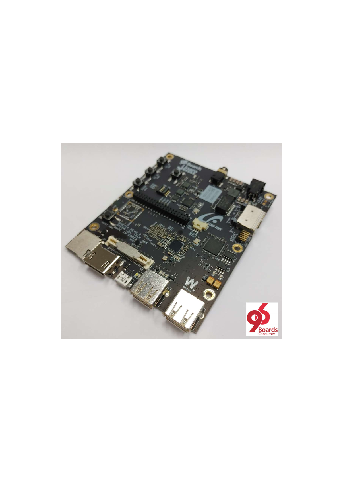
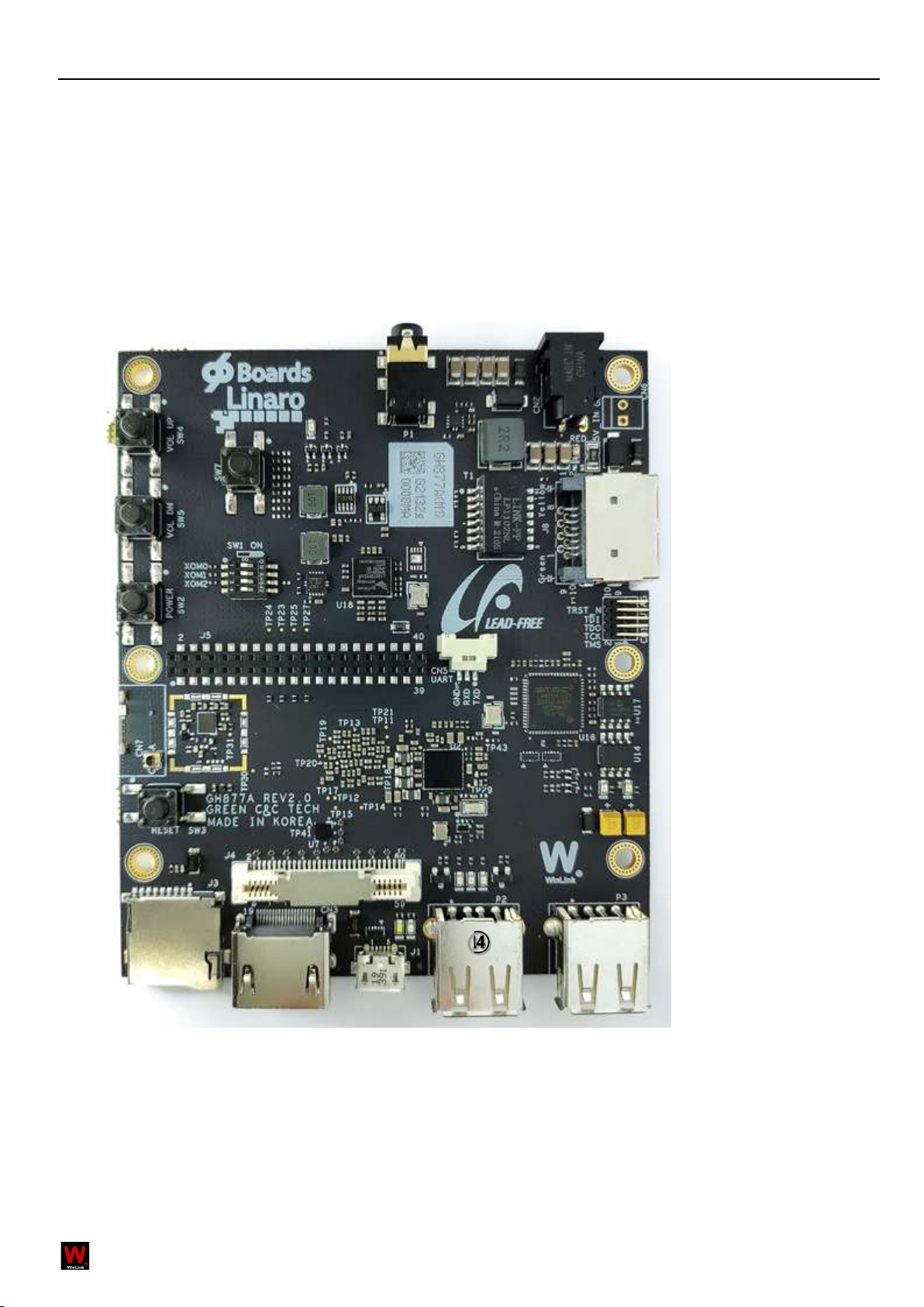
Board Overview ............................................................................................................................................................................ 5
Key Components ........................................................................................................................................................................... 6
System Block Diagram .................................................................................................................................................................. 7
Getting Started ............................................................................................................................................................................. 7
Prerequisites ......................................................................................................................................................................... 7
Starting the board for the first time ..................................................................................................................................... 7
Component Details ....................................................................................................................................................................... 8
Processor .............................................................................................................................................................................. 8
PMIC ..................................................................................................................................................................................... 8
Memory (DRAM) .................................................................................................................................................................. 8
Storage.................................................................................................................................................................................. 8
Micro SDHC ........................................................................................................................................................................... 8
Boot ROM ............................................................................................................................................................................. 8
Networking ........................................................................................................................................................................... 8
WiFi ....................................................................................................................................................................................... 8
Bluetooth .............................................................................................................................................................................. 9
HDMI .................................................................................................................................................................................... 9
MIPI-DSI ................................................................................................................................................................................ 9
Camera Interface .................................................................................................................................................................. 9
USB Ports .............................................................................................................................................................................. 9
USB Host ports.................................................................................................................................................................... 10
USB Device ports ................................................................................................................................................................ 10
Audio .................................................................................................................................................................................. 10
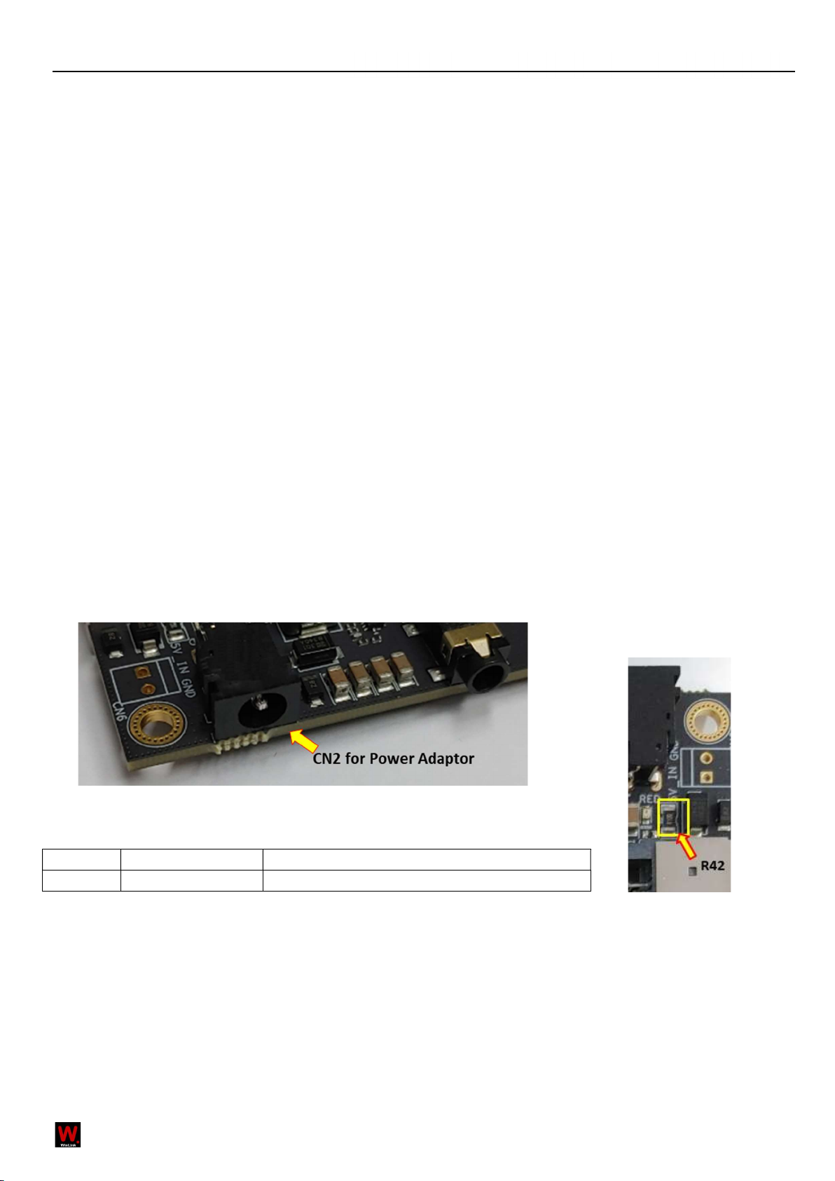
DC Power ............................................................................................................................................................................ 10
Power Measurement .......................................................................................................................................................... 10
UART ................................................................................................................................................................................... 10
Buttons ............................................................................................................................................................................... 11
LED Indicators ..................................................................................................................................................................... 12
Additional Functionality ..................................................................................................................................................... 12
Expansion Connectors ................................................................................................................................................................ 14
Low Speed Expansion Connector ....................................................................................................................................... 14
High Speed Expansion Connector ...................................................................................................................................... 16
Audio Connector................................................................................................................................................................. 18
Power Management Overview ................................................................................................................................................... 19
Block Diagram ..................................................................................................................................................................... 19
DC Power Input ................................................................................................................................................................... 19
Voltage Rails ....................................................................................................................................................................... 20
Mechanical specification ............................................................................................................................................................ 21

E850
-
96Board
Development
Board Hardware User Guide
WinLink
3/21
Introduction
The WinLink E850 Development Board is a 96Boards compliant community board based on Samsung Exynos 850 platform.
The following table lists its key features:
Processor
Samsung Exynos 850, S5E3830
Octa-core ARM@Cortex-A55 operating at up to 2.0GHz
• 32/32KB I/D Cache, 512KB+512KB L3 Cache
• 128 generic interrupt sources supported in legacy interrupt mode
• Coresight subsystem and Secure JTAG
ARM Mail G52MP1, operating at up to 700MHz
(Mali-G52 GPU with wide range of APIs such as OpneGL ES1.1/2.0/3.2, OpenCL 2.0 Full Profile
and Vulkan 1.0/1.1.)
Memory/
Storage
4GB LPDDR4x, 2CH, 16 bits up to 2133MHz (LPDDR4-4266)
64GB on board MCP, eMMC5.1
SD 3.0(Micro SD card slot )
Video
Multi-format Hardware Codec V10.21
• Decoding up to 1920x1080@60 fps for H.264/HEVC
• Decoding up to 1920x1080@30 fps for MPEG4/H.263/MPEG2/VC-1/VP8
• 20 Mbps for H.264/HEVC/MPEG4/H.263/MPEG2/VC-1/VP8
• Encoding up to 1920x1080@60 fps for H.264/HEVC
• Encoding up to 1920x1080@30 fps for MPEG4/H.263/VP8
• 20 Mbps for H.264/HEVC/MPEG4/H.263/VP8
Camera Support
2 MIPI CSI-2 ports available on board. (Main CSI0 : 4-lane, CSI1 : 2-lane 4-lane. )
Main camera IO supports 21.7MP @30fps.
Moving picture performance of FHD@30fps.
• Low-power Zero Shutter Lag(ZSL)
• Sensor defect compensation
3A-Statistics/Demosaicing/Denoising.
• Bayer down scaler
• Dynamic Range Compression
• Optical Distortion Correction
Connectivity
Samsung SoC, S5N5C12A01-6630(aka. S612)
WLAN 802.11a/b/g/n 2.4GHz and 5GHz(On-board BT and WLAN antenna )
Bluetooth BR/EDR and Low Energy v5.0
One USB 2.0 micro B (device mode only)
Two USB 2.0 (host mode only)
One 10/100Mbps Ethernet RJ-45 Connector
I/O Interfaces
One 40-pin Low Speed (LS) expansion connector
• UART, SPI, I2S, I2C x2, GPIO x12, DC power
One 60-pin High Speed (HS) expansion connector
• 4L-MIPI DSI, USB, I2C x2, 2L+4L-MIPI CSI
One 16-pin analog expansion connector for stereo headset/ line-out, speaker and analog line-in
External Storage
Micro SD card slot (SD3.0)
User Interface
4 Buttons :Power/Reset/Volume Up/down
6 LED indicators
• 4 -user controllable
• 2 -for radios (BT and WLAN activity)
OS
-
support
AOSP based on Android 10.0 k4.14
Power
Power: +12V to +18V
Mechanical
Dimensions: 85mm by 100mm of 96Boards™ Consumer Edition extended dimensions
specifications.
Environmental
Operating Temp: 0°C to +65°C RoHS and Reach compliant

E850
-
96Board
Development
Board Hardware User Guide
WinLink
4/21
What’s in the Box
The box contains one WinLink E850 Development Board.
Power Adaptor for E850 board also provided.
Documents and downloads available at;
https://www.96boards.org/documentation/consumer/e850-96b/

E850
-
96Board
Development
Board Hardware User Guide
WinLink
5/21
E850-96
Development Board
Board Overview
⑤
④
⑥
⑫
⑭
⑬
⑧
⑦
⑮
⑩
⑪
○
20
○
16
○
17
○
18
○
19
○
21
○
22
○
23
○
24
① +②
③

E850
-
96Board
Development
Board Hardware User Guide
WinLink
6/21
Key Components
Position
Reference Description
1
U1
Samsung Exynos 850 SoC
(Bottom Side)
2
U
10
8GB
/64GB
eMCP
(Bottom side)
3
U
12
W
IFI/Bluetooth S612
4
U2
PMIC
(
S2MPU12
)
5
J5
Low Speed Expansion Connector
6
J4
High Speed Connector
7
CN
7
Bluetooth/WLAN Antenna
8
J3
Micro SD Card Socket
9
CN
3
HDMI Type A Port
10
T1
R
J
-
45
11
J
1
Micro USB Type B Connector
12
LED
7
LED8
LED9
LED10
LED11
Hearbeat
LED
(Yellow)
eMMC LED(Yellow)
SD LED(White)
WiFi LED(Yellow)
Bluetooth LED(Blue)
13
P2
USB Host
1
Connector
14
P3
USB Host
2
Connector
15
S
W1
B
oot&
USB Host mode switch
16
U
16
U
SB
-
Ethernet Combo Hub IC
17
U
9
HDMI
IC (Bottom side component)
18
U
18
G
TI NPU
1
9
U
7
M
IPI
MUX switch
2
0
CN2
Power Outlet
2
1
S
W4
P
ower Key
2
2
K
1
R
eset Key
2
3
S
W2
V
OL UP(+)
2
4
S
W3
V
OL DN(
-
)

E850
-
96Board
Development
Board Hardware User Guide
WinLink
7/21
System Block Diagram
Getting Started
Prerequisites
Before you power up your WinLink E850 Development Board for the first time you will need the following:
WinLink E850 Development Board .
A 96Boards compliant power supply (included in box ).
A LCD Monitor that supports a HDMI/DVI interface with resolution of 1080P/60Hz.
HDMI-HDMI cable or HDMI-DVI cable to connect the board to the Monitor.
A computer keyboard with USB interface. A computer mouse with USB interface.
Starting the board for the first time
To start the board, follow these simple steps:
Step.1) Connect the HDMI cable to the WinLink E850 Development Board HDMI connector and to the LCD Monitor.
Step.2) Set the the second & third pin of switch SW1 to the position ON and connect the keyboard to USB connector marked
P2 and the mouse to the USB connector marked P3.(It doesn’t matter which order you connect them in. )
Step.3) Plug the power supply into the power outlet.
Step.4) Press down the button (marked SW2), and keep more than 3 seconds, the Android system will start.

E850
-
96Board
Development
Board Hardware User Guide
WinLink
8/21
Component Details
Processor
Exynos 850 is a System-on-Chip(SoC) based on 64-bit RISC cost-effective, low-power, high-performance optimized Little
Cortex-A55 Octa micro-processor for smart phone, tablet and also embedded applications
Exynos 850 supports 64-bit code with Cortex-A55 octa-core with LPDDR4x 2-channels, provides the Mali-G52 MP1 GPU with
wide range of APIs as OpenGL ES 1.1/2/0/3.2, OpenCL 2.0 Full Profile and Vulkan 1.0/1/1. This processor supports
FHD+(1080x2520) resolution.
Exynos 850 has an integrated Image Signal Processor(ISP). Dual camera scenario supports with single 21.7mega pixel@30fps
and dual 16+5 mega pixels @30fps preview w/BDS. ISP provides zero-shutter lag of camera shooting. Sensor defect
compensation, Dynamic range compression and Geometric distortion correction can be also supported.
PMIC
There are a PMIC and two dedicated DC - DC converters for Exynos 850 platform.
S2MPU12 is a power management system chip, containing 5 buck converters , 1 high efficient boost converter and 36
LDOs(22 PMOS LDOs, 14 NMOS LDOs).
S2MPU12 supports following Audio CODEC:
• Audio performance
- 84/89 dB SNR : Stereo audio ADC output for MIC input with 20dB/0dB gain setting
- 120/120/99/97 dB SNR : DAC to Stereo Headphone/Mono line & Earpiece & Speaker
- AVC (Adaptive Volume control) for a DAC to HP path for increases dynamic range
• Audio interface
Memory (DRAM)
The WinLink E850 Development Board provides 4GB LPDDR4-SDRAM which is a 2-channel and 32bit width bus
implementation interfacing directly to the Exynos 850 build-in LPDDR controller. The DDR clock is up to 2133MHz. It is
mounted on E850 96Board.
Storage
The WinLink E850 Development Board provides an 64GB flash memory which is compliant with eMMC 5.1.
Micro SDHC
The WinLink E850 Development Board SD slot signals are routed directly to the Exynos 850’s XMMC_CARD interface. It
meets the SD3.0 standard.
Boot ROM
The WinLink E850 Development Board boots up from the eMMC.
Networking
WiFi
Supports dual-band (2.4/5GHz) single stream 802.11 ac mode. (20/40/80MHz bandwidth)
Highly integrated front-end eliminates external PA and LNA matching.
Concurrent WLAN + BT reception.
Integrated power detector to support per packet Tx power control
The WinLink E850 Development Board also has a RF connector to connect the external antenna or other RF device. If you
want to use this function, you should put the cable to CN7 connector(MS-156C2:Hirose). It will automatically switch RF input
from chip antenna(ANT1) to connected device(CN7).

E850
-
96Board
Development
Board Hardware User Guide
WinLink
9/21
Bluetooth
Include RF transceiver, mixed ADC/DAC and baseband modem for BT5.0
Support for BT-WLAN coexistence operation, including concurrent receive via shared LAN with WLAN.
Support for class 1 and class 2 power-level transmissions without requiring an external PA.
HDMI
The 96Boards specification calls for an HDMI port to be present on the board. The Exynos 850 doesn’t include a built-in
HDMI interface. The WinLink E850 Development Board deploys the built-in DPI interface as the source for the HDMI output.
A peripheral Bridge IC (U9, LT8912B) performs this task and it supports a resolution from 480i to 1080p at 60Hz.
MIPI-DSI
The 96Boards specification calls for a MIPI-DSI implementation via the High Speed Expansion Connector.
The WinLink E850 Development Board implements a 4-lane MIPI_DSI interface meeting this requirement. It can support up
to FHD(1080p@60fps). The WinLink E850 Development Board routes the MIPI_DSI interface signals to the XMIPI_DSI4L
interface of the Exynos 850.
Camera Interface
The 96Boards specification calls for two camera interfaces.
The WinLink E850 Development Board supports two camera interfaces, one with a 4-lane MIPI_CSI interface and one with 2-
lane MIPI_CSI interface, meeting this requirement. The 4-lane MIPI_CSI interface can support 25M camera and the 2-lane
MIPI_CSI interface can support 8M camera.
* CN4 connector is also provided for 2-lane MIPI_CSI with I2C4 control signals.
Pin #
Pin Name Pin name in E850 SoC
1
GND
GND(1,4,7,10)
2
MIPI_CSI4LB_D0_N
XMIPI_CSI4LB_D0_N
3
MIPI_CSI4LB_D0_P
XMIPI_CSI4LB_D0_P
4
GND
GND
5
MIPI_CSI4LB_D1_N
XMIPI_CSI4LB_D1_N
6
MIPI_CSI4LB_D1_P
XMIPI_CSI4LB_D1_P
7
GND
GND
8
MIPI_CSI4LB_CLK_N
XMIPI_CSI4LB_CLK_N
9
MIPI_CSI4LB_CLK_P
XMIPI_CSI4LB_CLK_P
10
GND
GND
11
CAM_GPIO
XGPIO5/GPG1[5]
12
CLK2/CSI2_MCLK
XCAM_MCLK2/GPC0[2]
13
I2C4_SCL
XHSI2C2_SCL/GPC1[5]
14
I2C4_SDA
XHSI2C2_SDA/GPC1[4
15
CAM_VDD_33
VLDO32_PMIC(3.3V,300mA)
MIPI_CSI interface of E850 SoC XMIPI_CSI4LB signals are mapped.
Connector Part # : 10031HR-H15G(15-pin 1.0mm pitch FFC receptacle.
(Compatible with RPi camera V2 & Arducam OV5647 module)
USB Ports
The WinLink E850 Development Board supports a USB device port and three USB host ports via a USB MUX(U6).
The input channel( D+/D-) of USB MUX is connected to the P0 port of the SOC Exynos 850, and the two output
channels(1D+/1D-,2D+/2D-) are connected to micro USB port and USB hub respectively. The three USB host ports are
connected to the downstream ports of the USB hub. The control of U6(TS3USB221A) is done via a SW1’s 1st pin
(HOST_SEL). When this signal is logic low, ‘0’, the USB data lines are routed to the Micro USB connector and XEINT4 pin of

E850
-
96Board
Development
Board Hardware User Guide
WinLink
10/21
Exynos 850 is set to low, ‘0’, an external interrupt for Exynos 850 SoC as device mode. When ‘HOST_SEL’ is logic level high,
‘1’, the USB data lines are routed to U16 (a 4-port USB HUB) and the Exynos 850 is set to host mode.
USB Host ports
The WinLink E850 Development Board supports three USB host port via a USB2.0 hub (U16 LAN9514). Its upstream signal is
connected to USB_P0 interface of Exynos 850.
Port 1 of the USB HUB is routed to P2, a Type ‘A’ USB Host connector
Port 2 of the USB HUB is routed to P3, a Type ‘A’ USB Host connector
Port 3 of the USB HUB is routed to the High Speed Expansion connector.
USB Device ports
The WinLink E850 Development Board implements a device port. The port is located at J1, a Micro USB type B. It is routed to
USB_P0 interface of Exynos 850.
Note: the board can work in one mode at a time, Host mode or Device mode, not both.
Audio
The WinLink E850 Development Board has four audio ports: BT, HDMI, PCM and analog port. The analog port which
connected to PMIC(U2:S2MPU12) includes a stereo handset IO outputs.
DC Power
The WinLink E850 Development Board can be powered by two ways:
12V to 18V supply from a dedicated DC jack(CN2)
12V to 18V supply from the DC_IN pins on the Low Speed Expansion Connector(J5)
Power Measurement
The WinLink E850 Development Board has current sense resistors R42.
Reference
Net
Description
R
42
V_
SYS
To measure the current of
V_
SYS
(
5V
)
power
UART
The WinLink E850 Development Board has two UART ports (UART1 / UART0), both present on the Low Speed Expansion
connector. They are routed to the UART1 and UART0 interface of Exynos 850 separately.

E850
-
96Board
Development
Board Hardware User Guide
WinLink
11/21
Buttons
The WinLink E850 Development Board presents four buttons. They are Power key, VOL up key, VOL down key and Reset key.
The power ON/OFF and RESET signals are also routed to the Low Speed Expansion connector.
Power Button
The push-button SW2 serves as the power-on/sleep button. Upon applying power to
the board, press the power button for more than 3 seconds, the board will boot up.
Once the board is running you can turn power-off by pressing the power button for
more than 3 seconds. If the board is in a sleep mode, pressing the power bottom will
wake up the board. Oppositely, if the board is in an active mode, pressing the power
bottom will change the board into sleep mode.
Volume up/down
The Volume UP button(SW4) and Volume Down button(SW5) can be used to control
the output speaker volume of the WinLink E850 Development Board.
Reset Button
The push-button SW3 serves as the hardware reset button.
Press the button, the system will be rebooted
DIP-switch
There is a four-channel dip-switch(SW1) on the board.(Default position is “OFF”.)
The Table below is for boot mode.
SW1:3
SW1:2
SW1:1
First Boot Device
XOM[2]
XOM[1]
XOM[0]
off
off
off
1st : eMMC, 2nd : USB
0
0
1
1st : USB
0
1
0
Reserved
0
1
1
1st : eMMC(on board memory)
3’b100~3’b111
Reserved

E850
-
96Board
Development
Board Hardware User Guide
WinLink
12/21
LED Indicators
The WinLink E850 Development Board has five LEDs.
Two activity LEDs: LED9, LED10
WiFi activity LED –The WinLink E850 Development Board drives this Yellow LED(LED10) via X4, an IO from Exynos 850.
BT activity LED –The WinLink E850 Development Board drives this Blue LED(LED11) via X3, an IO from Exynos 850.
Three LEDs:
The three user LEDs are surface mount Green in 0603 size located next to the micro USB connector. The WinLink E850
Development Board drives the three LEDs from the Exynos 850 XGPIOs;
X1 : XGPIO10/GPG2[2] – Heart beat LED
X2 : XGPIO11/GPG2[3] – eMMC access/write LED
X3 : XGPIO12/GPG2[4] – SD access/write LED
Additional Debug Functionality
The WinLink E850 Development Board also has JTAG interface (CN1) for user debugging.
CN1 is 0.05” 10-pin angle-type pin header populated.
UART0 for debug console connector(CN5). The CN5 is 12507WR-03L SMD 1.25mm 3-pin SMD Connector. The UART0 Tx/Rx
pins are also available in LS 40-pin expansion connector for 96Boards interface SPEC.

E850
-
96Board
Development
Board Hardware User Guide
WinLink
13/21
CN5 : 12507WR-03L(YEONHO, 3-pin 1.25mm)
Mating connector : 12505HS-03(YEONHO), 51021-0300(Molex)

E850
-
96Board
Development
Board Hardware User Guide
WinLink
14/21
Expansion Connectors
Low Speed Expansion Connector
The following tables show the Low Speed Expansion Connector pin out:
PIN
96Boards Signals
WinLink
E850
Development Board Signals
Note
(Exynos 850 pin)
1
GND
GND
G
ND
3
UART0_CTS
L
S_UART0_CTS
XUSI_CMGP0_CTSN_CSN
5
UART0_TxD
LS_UART0_TxD
XUSI_CMGP0_TXD_DO_SDA0
7
UART0_RxD
LS_UART0_RxD
XUSI_CMGP0_RXD_CLK_SCL0
9
UART0_RTS
L
S_UART0_RTS
XUSI_CMGP0_RTSN_DI
11
UART1_TxD
UART1_TxD
UART_
DEBUG_1_
TxD
13
UART1_RxD
UART1_
R
xD
UART_DEBUG_1_
RxD
15
I2C0_SCL
I2C0_SCL
XI2C0_S
CL
17
I2C0_SDA
I2C0_S
DA
XI2C0_SD
A
19
I2C1_SCL
I2C
1
_SCL
XI2C1_S
CL
21
I2C1_SDA
I2C
1
_S
DA
XI2C1_SDA
23
GPIO
-
A
GPIO
-
A
XEINT
9
/GPA
1
[
1
]
25
GPIO
-
C
GPIO
-
C
XEINT1
0
/GPA
1
[
2
]
27
GPIO
-
E
GPIO
-
E
XEINT
11
/GPA
1
[
3
]
29
GPIO
-
G
GPIO
-
G
XEINT
22
/GPA2[
6
]
31
GPIO
-
I
GPIO
-
I
XEINT
24
/GPA
3
[
0
]
33
GPIO
-
K
GPIO
-
K
XEINT
26
/GPA
3
[
2
]
35
+1V8
V
LDO14_
PM
IC
VLDO14_PMIC
37
+5V
V_
SYS
39
GND
GND
G
ND
2
GND
GND
G
ND
4
PWR_BTN_N
PWRKEY
PWR
ON
(U2, PMIC)
6
RST_BTN_N
SYSRSTB
8
SPI0_SCLK
SPI0_CK
10
SPI0_DIN
SPI0_MI
12
SPI0_CS
SPI0_CS
14
SPI0_DOUT
SPI0_MO
16
PCM_FS
PM
_I2S
0_SYNC
18
PCM_CLK
PM
_I2S
0_
B
20
PCM_DO
PM
_I2S
0_DO
22
PCM_DI
PM
_I2S
0_DI
24
GPIO
-
B
GPIO
-
B
XEINT17/GPA2[1]
26
GPIO
-
D
GPIO
-
D
XEINT1
9
/GPA2[
3
]
28
GPIO
-
F
GPIO
-
F
XEINT
21
/GPA2[
5
]
30
GPIO
-
H
GPIO
-
H
XEINT
23
/GPA2[
7
]
32
GPIO
-
J
GPIO
-
J
XEINT
25
/GPA
3
[1]
34
GPIO
-
L
GPIO
-
L
XEINT
27
/GPA
3
[
3
]
36
SYS_DCIN
DC_IN
38
SYC_DCIN
DC_IN
40
GND
GND

E850
-
96Board
Development
Board Hardware User Guide
WinLink
15/21
UART {0/1}
The 96Boards specifications calls for a 4-wire UART implementation, UART0 and an optimal second 2wire UART, UART1 on
the Low Speed Expansion Connector.
The WinLink E850 Development Board implements UART0 as a 4-wire UART that connects directly to the Exynos 850 SoC.
These signals are driven at 1.8V.
The WinLink E850 Development Board implements UART1 as a 2-wire UART that connects directly to the Exynos 850 SoC.
These signals are driven at 1.8V.
I2C {0/1}
The 96Boards specification calls for two I2C interfaces to be implemented on the Low Speed Expansion Connector.
The WinLink E850 Development Board implements both interfaces named I2C4 and I2C5. They connect directly to the
Exynos 850 SoC. Each of the I2C lines is pulled up to VIO18_PMU via 4.7K resistor.
GPIO {A-L}
The 96Boards specification calls for 12
GPIO lines to be implemented on the
Low Speed Expansion Connector.
All GPIO pins could be used as external
interrupt sources. GPIO A ~ L are routed
to the Exynos 850 SoC.
Note 1) When a port is used as an output function, DISABLE the pull-up/down.
Note 2) All GPIOA~L Pull Down with 50k internally by default
SPI 0
The 96Boards specification calls for one SPI bus master to be provided on the Low Speed Expansion Connector.
The WinLink E850 Development Board implements a full SPI master with 4 wires, CLK, CS, MOSI and MISO. The signals are
connected directly to the Exynos 850 SoC and driven at 1.8V.
PCM/I2S
The 96Boards specification calls for one PCM/I2S bus to be provided on the Low Speed Expansion Connector. The CLK, FS
and DO signals are required while the DI is optional.
The WinLink E850 Development Board implements a PCM/I2S interface with 4 wires, CLK, FS, DO and DI. The signals are
connected directly to the Exynos 850 SoC and driven at 1.8V.
Power and Reset
The 96Boards specification calls for a signal on the Low Speed Expansion Connector that can power on/off the board and a
signal that serves as a board reset signal.
The WinLink E850 Development Board routes the PWR_BTN_N (named POWERKEY on schematic) signal to the PWRON pin
of the PMIC S2MPU12. This signal is driven by SW4 as well, the on-board power on push-button switch. A mezzanine
implementation of this signals should not drive it with any voltage, the only allowed operation is to force it to GND to start
the board from a sleep mode.
The WinLink E850 Development Board routes the RST_BTN_N (named XNWRESET on schematic) signal to the WRSTBO pin of
the PMIC S2MPU12.
E850 96 Board GPIO Signals
Exynos 850 pin Remarks
GPIO
-
A
XEINT
9
/GPA
1
[
1
]
VDDQ18_ALIVE(
1
.8V) signal
GPIO
-
C
XEINT1
0
/GPA
1
[2]
VDDQ18_ALIVE(
1
.8V) signal
GPIO
-
E
XEINT
11
/GPA
1
[
3
]
VDDQ18_ALIVE(
1
.8V) signal
GPIO
-
G
XEINT22/GPA2[6]
VDDQ18_ALIVE(
1
.8V) signal
GPIO
-
I
XEINT24/GPA3[0]
VDDQ18_ALIVE(
1
.8V) signal
GPIO
-
K
XEINT26/GPA3[2]
VDDQ18_ALIVE(
1
.8V) signal
GPIO
-
B
XEINT17/GPA2[1]
VDDQ18_ALIVE(
1
.8V) signal
GPIO
-
D
XEINT19/GPA2[3]
VDDQ18_ALIVE(
1
.8V) signal
GPIO
-
F
XEINT21/GPA2[5]
VDDQ18_ALIVE(
1
.8V) signal
GPIO
-
H
XEINT23/GPA2[7]
VDDQ18_ALIVE(
1
.8V) signal
GPIO
-
J
XEINT25/GPA3[1]
VDDQ18_ALIVE(
1
.8V) signal
GPIO
-
L
XEINT27/GPA3[3]
VDDQ18_ALIVE(
1
.8V) signal

E850
-
96Board
Development
Board Hardware User Guide
WinLink
16/21
Power Supplies
The WinLink E850-96Boards specification calls for three power rails to be present on the Low Speed Expansion Connector:
+1.8V Max of 100mA
+5V Provide a minimum of 7.5W of power (2.5A).
SYS_DCIN 12-18V input with enough current to support all the board functions.
The WinLink E850 Development Board supports these requirements as follows:
+1.8V : Driven by PMIC S2MPU12 up to 450mA. It is the system IO power (VLDO14_PMIC), and it can supply power up to
450mA to the Low Speed Expansion Connector.
+5V : Driven by a 8A System DC-DC buck converter (U4). It also provides the VBUS power to the two USB host
connectors (P2, P3) and the HDMI 5V power to the HDMI connector (CN3).The remaining capacity provides a max current
of 2A to the Low Speed Expansion Connector, for a total of 10W which meets the 96Boards requirements.
SYS_DCIN Can serves as the board’s main power source or can receive power from the board.
High Speed Expansion Connector
PIN
96Boards Signals
WinLink
E850
Development Board
Signals
Note
1
SD_DAT0/SPI1_DOUT
SPI1_MO
3
SD_DAT1
NC
5
SD_DAT2
NC
7
SD_DAT3/SPI1_CS
SPI1_CS
9
SD_SCLK/SPI1_SCL
SPI1_CK
11
SD_CMD/SPI1_DIN
SPI1_MI
13
GND
GND
15
CLK0/CSI0_MCLK
CAM_CLK0
17
CLK1/CSI1_MCLK
CAM_CLK1
19
GND
GND
21
DSI_CLK+
TCP
23
DSI_CLK
-
TCN
25
GND
GND
27
DSI_D0+
TDP0
29
DSI_D0
-
TDN0
31
GND
GND
33
DSI_D1+
TDP1
35
DSI_D1
-
TDN1
37
GND
GND
39
DSI_D2+
TDP2
41
DSI_D2
-
TDN2
43
GND
GND
45
DSI_D3+
TDP3
47
DSI_D3
-
TDN3
49
GND
GND
51
USB_D+
USB_DP_P1_EXP
53
USB_D
-
USB_DM_P1_EXP
55
GND
GND
57
HSIC_STR
NC
59
HSIC_DATA
NC

E850
-
96Board
Development
Board Hardware User Guide
WinLink
17/21
High Speed Expansion Connector(Cont’d)
PIN
96Boards Signals
WinLink
E850
Development Board Signals
Note
2
CSI0_C+
RCP
4
CSI0_C
-
RCN
6
GND
GND
8
CSI0_D0+
RDP0
10
CSI0_D0
-
RDN0
12
GND
GND
14
CSI0_D1+
RDP1
16
CCSI0_D1
-
RDN1
18
GND
GND
20
CSI0_D2+
RDP2
22
CSI0_D2
-
RDN2
24
GND
GND
26
CSI0_D3+
RDP3
28
CSI0_D3
-
RDN3
30
GND
GND
32
I2C2_SCL
SCL2
34
I2C2_
SDA
SDA2
36
I2C3_
SCL
SCL3
38
I2C3_SDA
SDA3
40
GND
GND
42
CSI1_D0+
RDP0_A
44
CSI1_D0
-
RDN0_A
46
GND
GND
48
CSI1_D1+
RDP1_A
50
CSI1_D1
-
RDN1_A
52
GND
GND
54
CSI1_C+
RCP_A
56
CSI1_C
-
RCN_A
58
GND
GND
60
RESERVED
Pull
-
up
to VIO18_PMU via 100K resistor
MIPI DSI 0
The 96Boards specification calls for a MIPI-DSI to be present on the High Speed Expansion Connector. A minimum of one
lane is required and up to four lanes can be accommodated on the connector.
The WinLink E850 Development Board implementation supports a full four lane (1.2Gbps/lane) MIPIDSI interface that is
routed to the High Speed Expansion Connector. The MIPI-DSI signals are directly connected to DSI-0 of Exynos 850.
MIPI CSI {0/1}
The 96Boards specification calls for two MIPI-CSI interfaces to be present on the High Speed Expansion Connector. Both
interfaces are optional. CSI0 interface can be up to four lanes while CSI1 is up to two lanes.
The WinLink E850 Development Board implementation supports a full four lane MIPI-CSI interface on
CSI0 and two lanes of MIPI-CSI on CSI1. All MIPI-CSI signals are routed directly to/from the Exynos 850 SoC.
CSI0 can support up to 25M@30fps and CSI1 can support up to 8M@30fps. The max data rate of each lane is 2.5Gbps.
I2C {2/3}
The 96Boards specification calls for two I2C interfaces to be present on the High Speed Expansion Connector. Both interfaces
are optional unless a MIPI-CSI interface has been implemented. Then an I2C interface shall be implemented.

E850
-
96Board
Development
Board Hardware User Guide
WinLink
18/21
The WinLink E850 Development Board implementation supports two MIPI-CSI interfaces and therefore must support two I2C
interfaces. For MIPI-CSI0 the companion I2C2 is routed directly from the EXYNOS 850SoC. For MIPI-CSI1, the companion I2C
is I2C3.
SD/SPI
The 96Boards specification calls for an SD interface or a SPI port to be part of the High Speed Expansion Connector.
The WinLink E850 Development Board implements a full SPI master with 4 wires (96Boards SPI Configuration), CLK, CS, MOSI
and MISO. All the signals are connected directly to the Exynos 850 SoC.
These signals are driven at 1.8V.
Clocks
The 96Boards specification calls for one or two programmable clock interfaces to be provided on the High Speed Expansion
Connector. These clocks may have a secondary function of being CSI0_MCLK and CSI1_MCLK. If these clocks can’t be
supported by the SoC than an alternative GPIO or No Connect is allowed by the specifications.
The WinLink E850 Development Board implements two CSI clocks which are connected directly to the Exynos 850 SoC. These
signals are driven at 1.8V.
USB
The 96Boards specification calls for a USB Data line interface to be present on the High Speed Expansion Connector.
The WinLink E850 Development Board implements this requirement by routing USB channel 3 from the USB HUB to the High
Speed Expansion Connector.
Reserved
The pin 60 of the High Speed Expansion Connector is pulled up to AVDD18_HSCON via R179 100K resistor.
Audio Connector
PIN 3.5mm Audio Receptacle (P1) Note : CTIA 3.5 Plug (Part # : APJ3-089S64)
1
EAR_MIC_P
Microphone p
ositive
in
put of
PMIC
’
s Audio Front
-
end (U2, S2MPU12)
2
PM_HPOUTL
Audio left
output from
PMIC
’
s Audio Front
-
end (U2, S2MPU12)
3
PM_HPOUTR
Audio right output from PMIC
’
s Audio Front
-
end (U2, S2MPU12)
4
GND
Ground
10
PM_HPL_DET
Audio
left
-
channel detection signal
of PMIC(U2, S2MPU12)
11
PM_HPG_DET
Audio GND detection signal of PMIC(U2, S2MPU12)

E850
-
96Board
Development
Board Hardware User Guide
WinLink
19/21
Power Management Overview
Block Diagram
DC Power Input
An 12V to 18V power from a dedicated DC jack CN2.
An 12V to 18V power from the SYS_DCIN pins on the Low Speed Expansion Connector J5.
Note: Please refer to the mechanical size of the DC plug
below. The inside diameter of the plug is 1.7mm,the outer
diameter of the plug is 4.75mm. The positive electrode of
the DC plug is in the inside, and the negative pole is outside.
Auxiliary 5V power supply available on CN6.

E850
-
96Board
Development
Board Hardware User Guide
WinLink
20/21
Voltage Rails
Circuit Type
Net Name Default ON
Voltage(V)
Iout Max
(mA) Connected Net(s)
Sys.BUCK V_SYS 5 8000 System Power : 5V (MP2386 output)
_CLK PMIC
BUCK1_PMIC 0.75 1500 VDD_CPU of Exynos 850
BUCK2_PMIC 0.75 4000 VDD_INT of Exynos 850
BUCK3_PMIC 0.75 3000 VDD_CP of Exynos 850,
VDD_WBG(WLBT : VDDQ18_WBG)
VLDO1_PMIC 0.75 300 VDD075_ALIVE, VDD075_TCXO, VDD_ALV_CP, VDD075_USB20
VLDO2_PMIC 1.8 450 VDDQ18_EXT , VDDQ18_ALIVE, VDDQ18_MMC_EMBD,
AVDD18_GPADC, VDDQ18_WBG, AVDD18_TCXO,
VDDP18_MMC_CARD, VDD1_MEM, VDD_EMMC_1P8,
VDD
18
_I2C, VDDQ18_PERI, VDD18_IO_WLBT
,
AVDD18_USB20
VLDO3_PMIC 0.85 300 VDD085_OTP, VDD085_PLL_CPUCL0, VDD085_PLL_CPUCL1,
VDD085_PLL_SHARED, VDD085_PLL_AUD,
VDD085_PLL_DDRPHY0/1,
VDD085_PLL_G3D, VDD085D_PLL_SHARED, VDD085D_PLL_AUD,
AVDD085_MIPI_CSI_DPHY, AVDD085_MIPI_DSI_DPHY
VLDO4_PMIC 1.8 150 AVDD18_PLL_CPUCL0/1, AVDD18_PLL_AUD,
AVDD18_PLL_SHARED, AVDD18_PLL_G3D,
AVDD18_MIPI_CSI_DPHY, AVDD18_MIPI_DSI_DPHY,
AVDD18_PLL_DDRPHY0/1, AVDD18_OTP, AVDD18_AUD_DET
VLDO5_PMIC 1.1 800 VDD2_MEM,
VDDQ11_DRAM0_CKE, VDDQ11_DRAM1_CKE
VLDO6_PMIC 0.6 600 VDDQ_MEM, VDDQ06_DRAM0, VDDQ06_DRAM1,
VDDQ06_DRAM0_CLK, VDDQ06_DRAM1_CLK
VLDO10_PMIC 1.8 150 VDDQ1833_MMC_CARD
VLDO11_PMIC 3.0 150 AVDD33_USB20
VLDO14_PMIC 1.8 450 AVDD18_CP, AVDD18_WLBT, AVDD18_HSCON, AVDD18_MUSB
AVDD18_HSCON@HS_CON(J4,
#60), LSCON(J5, #35)
VLDO24_PMIC 3.0 800 VDD_LAN
VLDO25_PMIC 1.8 150 VDD_T_FLASH_3V0
VLDO27_PMIC 3.0 180 MIPI_SWITCH_3V3
VLDO28_PMIC 1.8 150 HDMI_CONV_1V8
VLDO30_PMIC 1.8 150 NPU_VDD18
VLDO32_PMIC 3.3 300 CAM_VDD
VLDO35_PMIC 1.8 150 DLDO_CORE_1P8
Other
PWR2_D 5 500 USB host1 output power protection(P2)
PWR3_D 5 500 USB host2 output power protection(P3)
VLDO14_PMIC 1.8 450 1.8V on LS connector(#35)
VOUT 5 8000 5V output of System BUCK(MP2386)
SYS_DCIN 8-18 3000 8-18V DCIN on LS connector(#36, #38)
Table of contents
Other 96Boards Motherboard manuals