Unicorn ENDAT-5701 User manual

ENDAT-5701/5901
All-In-One motherboard
User’s Manual
Rev. 3x
For 5701 PCB ver.1F or later
For 5901 PCB ver.2xor later
4/30/2002
II
The ENDAT-5701/5901 All-In-One motherboard
Copyright Notice
The content of this manual has been checked for accuracy. The manufacturer
assumes no responsibility for any inaccuracies that may be contained in this
manual. The manufacturer reserves the right to make improvements or
modification to the this document and/or the product at any time without prior
notice. No part of this document may be reproduced, transmitted, photocopied or
translated into any language, in any form or by any means, electronic, mechanical,
magnetic, optical or chemical, without the prior written permission of the
manufacturer.
VIA is registered trademark of VIA Technology Incorporation
VIA Apollo MVP4 may only be used to identify products of VIA Technology
VT82C868A may only be used to identify products of VIA Technology
Realtek is registered trademark of Realtek Technologies Inc.
Multiscan is a trademark of Sony Corp of America
IBM, EGA, VGA, PC/XT, PC/AT, OS/2 and PS/2 are registered trademarks of
International Business Machines Corporation
Intel is a registered trademark of Intel Corporation
Plug and Play is registered trademarks of Intel Corporation
Microsoft, Windows and MS-DOS are trademarks of Microsoft Corporation
Award is a trademark of Award Software Inc.
PCI is a registered trademark of PCI Special Interest Group
Other product names mentioned herein are used for identification purpose only
and may be trademarks and/or registered trademarks of their respective
companies.
Installation Notice
The manufacturer recommends using a grounded plug to ensure proper
motherboard operation. Care should be used in proper conjunction with a
grounded power receptacle to avoid possible electrical shock. All integrated
circuits on this motherboard are sensitive to static electricity. To avoid damaging
components from electrostatic discharge, please do not remove the board from the
anti-static packing before discharging any static electricity to your body, by
wearing a wrist-grounding strap. The manufacturer is not responsible for any
damage to the motherboard due to improper operation.

User’s Manual III
Specification:This manual covers two different layout model of
Pentium embedded motherboard. The respective board layout outlines are
shown on Chapter 1-4/1-5. Please refer to the following description to make
sure which model you have before using.
MODEL ENDAT-5701 ENDAT-5901
CPU Pentium 75-550MHz,
INTEL MMX, AMD K5/K6/K6-2/K6-3,
IDT C6, Rise MP6, IBM Cyrix 6x86 CPU
System Chipset VIAChipset
VGA Chipset Built-in, With Share Memory Architecture
LCD Feature (Optional) Optional Support TFT/ DSTN LCD
LAN Chipset Realtek 8139A/B/C 10BaseT/100 BaseT(Boot ROM Optional)
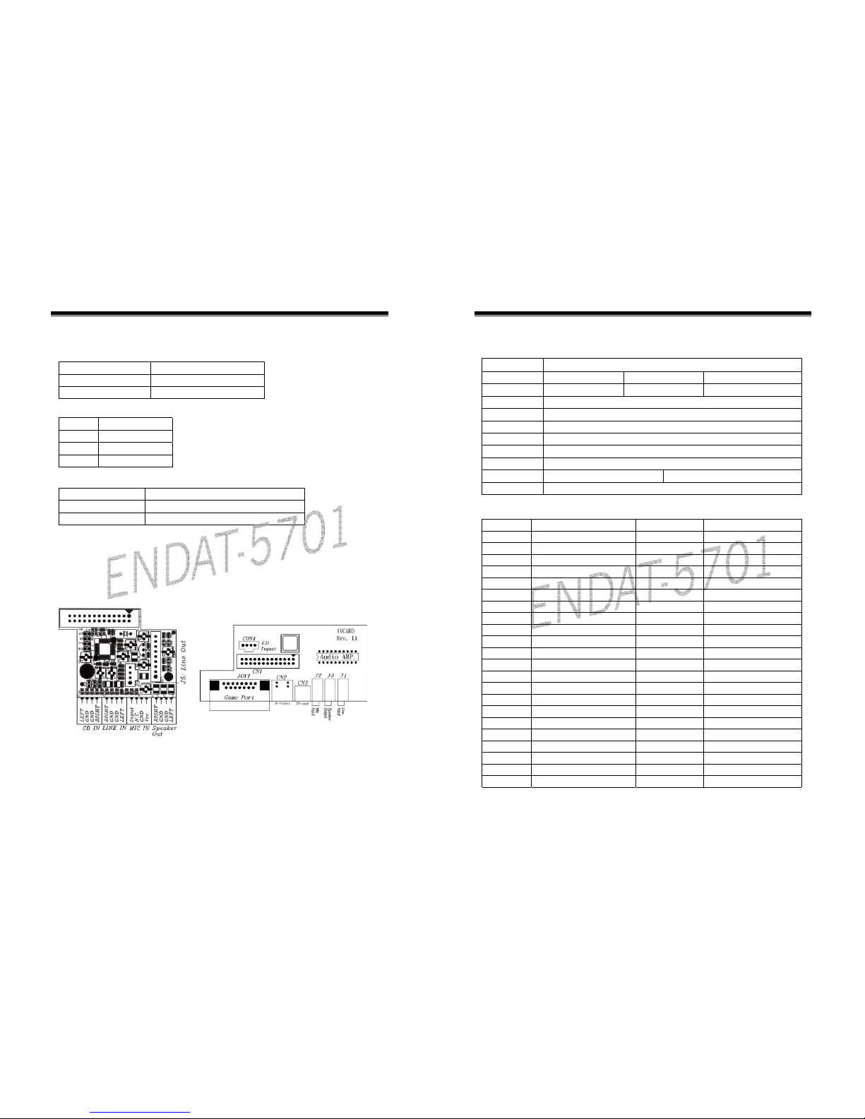
Audio Feature (Optional) via AV Card kit
TV-Out (Optional) via AV Card kit
FLASH Disk Socket for DiskOnChip
System Memory Upto 512MB(PC66/PC100)
IDE Interface PCI IDE Support Ultra DMA33/66
Multi I/O Supports 4 Serial and 1 Parallel Ports
COM1, 3, 4 with +5V/+12V Power
Supports RS422/485 for COM2 (Optional)
External Cache 512KB Burst Cache
IrDA / USB Port Yes(Pin Header)
Expansion Slot Extension for PCI/ISA Bus
AD Selector PCI 1
PCI 2
PCI 3
PCI 4
AD24 LAN (INT.A,B,C,D)
AD23 FREE (INT.B,C,D,A)
AD22 FREE (INT.C,D,A,B)
AD21 FREE (INT.D,A,B,C)
Location of Expansion
Slot At the 7
th
of Standard AT MB At the 6
th
of Standard AT MB
Keyboard / Mouse Jack Two Mini Din Jack and Pin Header
Pin Header for Keyboard / Mouse / VGA / Multi I/O ports
Power Connector PS/2 and ATX Type
Form Factor WD/LPX (220x220mm) PC/AT (223x220mm)
IV
The ENDAT-5701/5901 All-In-One motherboard
TABLE OF CONTENTS
CHAPTER 1. INTRODUCTION.................................................1
1-1. FEATURES .............................................................................................1
1-2. UNPACKING..........................................................................................3
1-3. ELECTROSTATIC DISCHARGE PRECAUTIONS.............................. 3
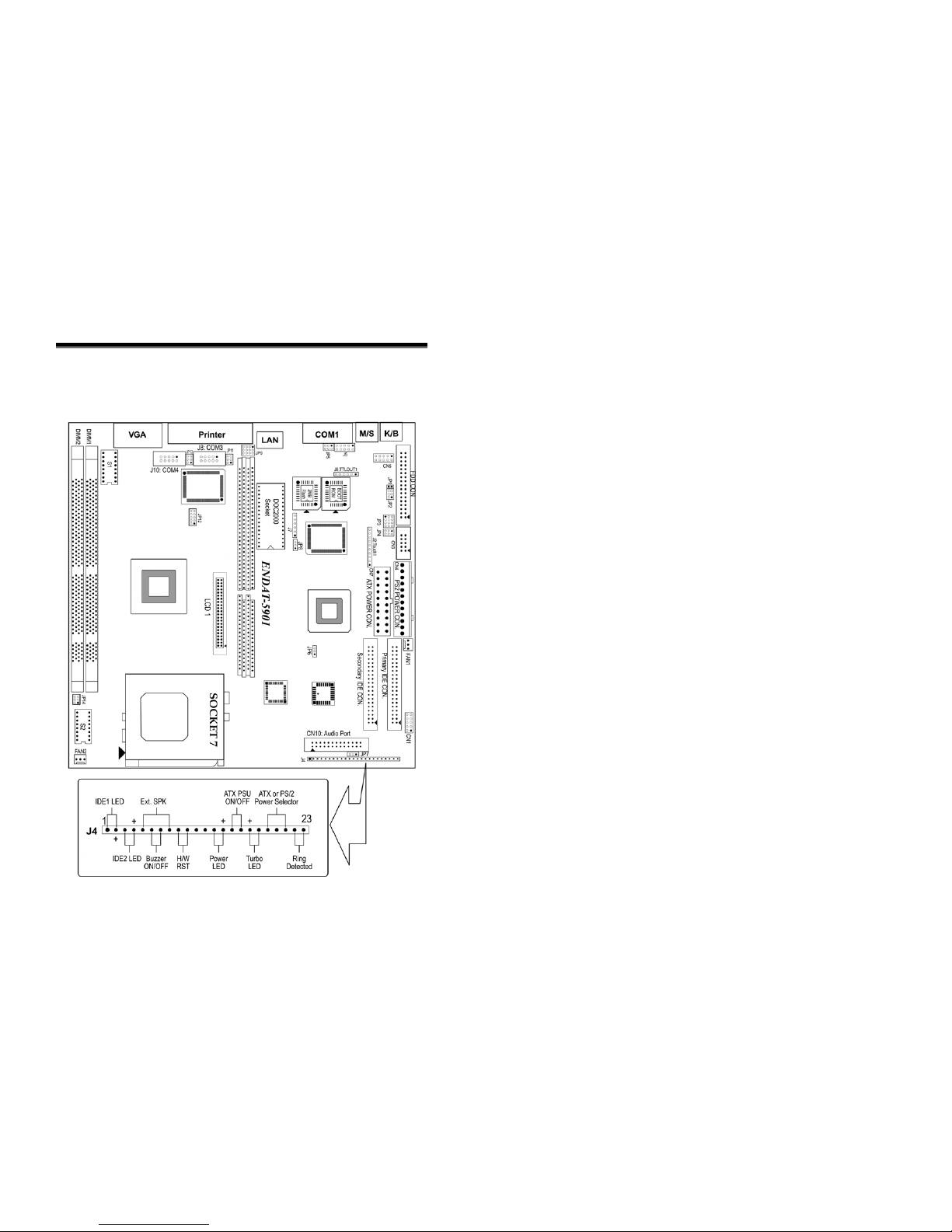
1-4. MOTHERBOARD LAYOUT (ENDAT-5701) ....................................... 4
1-5. MOTHERBOARD LAYOUT (ENDAT-5901) ....................................... 5
CHAPTER 2. SETTING UP THE MOTHERBOARD..............7
2-1. JUMPERS AND CONNECTORS (ENDAT-5701) .................................7
2-2. JUMPERS AND CONNECTORS (ENDAT-5901) ..............................16
2-3. INSTALLING MEMORY ...................................................................... 25
2-4. SHARED VGA MEMORY....................................................................25
2-5. INSTALLING RISER CARD ................................................................ 25
2-6. ASSIGNING IRQs FOR EXPANSION CARDS................................... 26
2-7. ASSIGNING DMA CHANNELS FOR ISA CARDS............................ 27
CHAPTER 3. AWARD BIOS SETUP........................................29
3-1. QUICK SETUP ...................................................................................... 29
3-2. DESCRIPTION OF BIOS SETUP OPTIONS....................................... 30
3-3. BIOS FEATURES SETUP..................................................................... 30
3-4. DETAILS OF CHIPSET FEATURE SETUP......................................... 31
3-5. DETAILS OF POWER MANAGEMENT SETUP................................ 33
3-6. PCI CONFIGURATION SETUP ........................................................... 36
3-7. SYSTEM ENVIRONMENT.................................................................. 37
3-8. INTEGRATED PERIPHERALS ........................................................... 38

User’s Manual V
CHPATER 4. VGA, FLAT PANEL, DOC, IDE FEATURE ....41
4-1. AGP-BUS VGA FEATURE .................................................................. 41
4-2. LCD FLAT PANEL FEATURE............................................................. 42
4-3. PCI BUS AUDIO ADAPTER FEATURE ............................................. 43
4-4. DISKONCHIP FEATURE..................................................................... 44
4-5. DRIVER UTILITY INSTALLATION GUIDE .................................... 45
CHPATER 5. LAN ADAPTER...................................................47
5-1. FEATURES............................................................................................ 47
5-2. UTP CABLE/RJ-45 JACK DEFINITION............................................. 48
5-3. CONNECTING 100BASE-TX FAST ETHERNET NETWORK ......... 49
5-4. CONNECTING 10BASE-T ETHERNET NETWORK ........................ 49
5-5. 10M BASE/100MBASE INSTALLATION NOTICE ........................... 49
5-6. REMOTE BOOT ROM INSTALLATION GUIDE............................... 50
5-7. LED INDICATORS............................................................................... 51
5-8. SETUP PROGRAM ............................................................................. 51
5-9. LAN DRIVER INSTALLATION PROCEDURE.................................. 54
APPENDIX A: FLASH MEMORY UTILITY .........................55
APPENDIX B: CONNECTOR PIN ASSIGNMENT ...............56
APPENDIX C: LIMITED WARRANTY ..................................64

Chapter 1. Introduction
The ENDAT-5701 and ENDAT-5901 All-In-One motherboard uses VIA chipsets
built-in VGA onboard supports TFT/DSTN Flat Panel and Audio, built-in Realtek
8139xx LAN chipset with RJ45 Jack for 10BaseT/100BaseT. Our board offers the
highest performance PC specifications in the industry. The ENDAT-5701 and
ENDAT-5901 runs with the Intel Pentium P54C/P55C, AMD K5/K6, K6-2/K6-3,
IDT C6, Rise MP6 or IBM/Cyrix 6x86 CPU upto 550MHz.
The motherboard is fully compatible with industry standards, adding many
technical enhancements and is fully compatible with thousands of software
applications developed for IBM PC/AT compatible computers. The control logic
provides high-speed performance for the most advanced multi-user, multitasking
applications available today. “Tomorrows PC technology is here today”.
1-1. Features
Basic Feature:
•
Supports all Socket-7 / Supper-7 Processors Including 64-bit Intel Pentium™,
Pentium™ MMX, AMD 6K86™, IDT C6, Rise MP6 and IBM/Cyrix 6x86 CPUs
Clock base on 60MHz ~ 100MHz “Front Side Bus”, supports upto 550MHz
•
PC-98/99 Compatible using VIA VT82C686A south bridge chip
•
Pipelined burst synchronous SRAM (PBSRAM) cache support, maximum 512KB
pipeline burst SRAM cache
•
Supports 64-bit DRAM interface synchronous with host CPU (66/100MHz) or
internal Memory Clock (100MHz)
•
Supports up to 512MB memory with two 168 pin DIMM socket (PC-100/66
DIMM)
•
Independent clock stop controls for CPU /SDRAM, Internal AGP and PCI bus
•
On board built-in PCI BUS master IDE control, supports up to five PCI bus and
floppy drive controller
2
ENDAT-5701 and ENDAT-5901 All-In-One motherboard uses
•
PCI-2.2 compliant, 32 bit 3.3V PCI interface with 5V tolerant inputs
•
Onboard socket for DiskOnChip supports M-System products
•
Onboard LAN Adapter supports 10BaseT/100BaseT, (On board) BOOT ROM
optional
•
Support for 4 COM ports, STD. RI(RS-232), COM1, 3, 4 with +12V/+5V DC
Power selectable and one SPP/EPP/ECP Parallel port.
•
Supports Ultra DMA33/66 EIDE
•
Onboard support for 4 high-speed UARTS (W/16550 FIFO) and multi-mode
•
Parallel port for standard, enhanced(EPP) and high-speed(ECP) mode
•
Onboard built-in USB functions
•
Onboard built-in 2x AGP VGA BUS adapter, AGP v2.0 compliant for 1x and 2x
transfer modes
•
188pin expansion slot for both PCI and ISA BUS signals
•
AWARD BIOS FLASH ROM (2Mbits)
•
IR function can be Enabled/Disabled by BIOS
•
Onboard LAN adapter can be Enabled/Disabled by jumper settings.
Optional Features
•
Supports with RS232/RS422/RS485 interface for COM2
•
Supports LCD feature with TFT/DSTN Panel
•
Supports Audio function with AV Card Kit
•
Supports TV-Out feature

User’s Manual 3
1-2. Unpacking
The motherboard comes securely packaged in a sturdy cardboard shipping carton.
In addition to the User's Manual, the motherboard package includes the following
items:
•
ENDAT-5701/ENDAT-5901 All-In-One Motherboard
•
HDC/FDC Cables
•
TV-Out Cable (Optional)
•
Audio Kit (Optional)
•
Serial port kit for 2 ports
•
IDE Driver includes: Drivers for Windows 3.1, Windows NT 3.x/4.x,
Windows 95, 98, 2000, Novell Netware and AWARD FLASH ROM
utilities.
•
VGA utilities and software drivers
•
Driver utilities for LAN adapter
If any of these items are missed or damaged, please contact the dealer from whom
you purchased the motherboard. Save the shipping materials and carton in the
event that you want to ship or store the board in the future.
Note:
Leave the motherboard in its original packing until you are ready to install it!
1-3. Electrostatic Discharge Precautions
Make sure you properly ground yourself before handling the motherboard, or other
system components. Electrostatic discharge can easily damage the components.
Note: You must take special precaution when handling the motherboard in dry or
air-conditioned environments.
4
ENDAT-5701 and ENDAT-5901 All-In-One motherboard uses
1-4. Motherboard Layout (ENDAT-5701)

User’s Manual 5
1-5. Motherboard Layout (ENDAT-5901)

Chapter 2. Setting up the Motherboard
This chapter describes how to set up the motherboard and get ready for operation.
•
Installing the CPU upgrade
•
Installing DIMM memory. Make sure the correct CPU operating
voltage, jumper settings and frequency.
•
Double-check the insertion and orientation of the CPU before applying
power. Improper installation will result in permanent damage to the
CPU.
2-1. Jumpers and Connectors (ENDAT-5701)
Jumpers/Connectors Overview:
Function Jumpers/Connectors
CPU: CPU Clock Frequency Switch 1 (S1: SW1-SW4)
CPU Vcore Voltage Switch 2 (S2: SW1-SW5)
CPU Ratio Switch 2 (S2: SW6-SW8)
Connector for Cooling Fan FAN1,FAN2
Power Supply: Type (ATX or PS/2) CN2(ATX);CN1(PS/2)
Power Good JP15
ATX or PS/2 Power Selector J3 Pin 19, 20, 21
ATX Power On/Off Switch J3 Pin 15, 16
Audio /TV-Out Output Port Connector CN7
LAN Adapter Disable/Enable JP4
PCI INT selector for Expansion Slot JP16
COM3 Port J5
COM4 Port J6
COM3/COM4 IRQ Setting BIOS Defined
COM Ports Power Selector (COM1, 3,4) JP6, JP12, JP13
8
ENDAT-5701 and ENDAT-5901 All-In-One motherboard uses
Function Jumpers/Connectors
RS232/RS422/RS485 Selector (COM2) JP7, JP8, JP9, JP10
TTL Output Pin Header (For COM2) TTLOut1
Touch Panel Pin Header Touch1
DiskOnChip Memory Address JP2
LCD Connector LCD_CON1
Clear CMOS JP1
PS/2 Keyboard Jack CN6
PS/2 Mouse Jack CN2
PS/2 Mouse/KB Pin Header CN4
IR IR1
USB Header CN11
FDD Connector CN5
IDE 1 J1
IDE 2 J2
Header for Case Panel J3
IDE 1 LED J3 Pin 1, Pin 2
IDE 2 LED J3 Pin 3, Pin 4
External Speaker J3 Pin 5, Pin 8
Buzzer On/Off J3 Pin 6, Pin 7
Hardware Reset Switch J3 Pin 9, Pin 10
Power LED J3 Pin 13, Pin 14
ATX Power Supply On/Off Switch J3 Pin 15, Pin 16
Turbo LED for Case (for case only, no function) J3 Pin 17, Pin 18
ATX or PS/2 Power Selector J3 Pin 19, Pin 20, Pin 21
Ring-Detected J3 Pin 22, Pin 23
Note:
The cooling fan and heat sink are required for Pentium processors. Please pay
close attention to the direction of the CPU and cooling fan when install. Position
the cooling ventilator directly facing the regulator heat sink, which is located
beside the CPU socket. This will reduce the overheating of the regulator and
increase the reliability of the system.

User’s Manual 9
ENDAT-5701 CPU Vcore Setting: Switch2 (S2: SW1-SW5)
VCORE=3.5V
S1 S2 S3 S4 S5
ON ON ON ON OFF
VCORE=3.4V
S1 S2 S3 S4 S5
OFF ON ON ON OFF
VCORE=3.3V
S1 S2 S3 S4 S5
ON OFF ON ON OFF
VCORE=3.2V
S1 S2 S3 S4 S5
OFF OFF ON ON OFF
VCORE=3.1V
S1 S2 S3 S4 S5
ON ON OFF ON OFF
VCORE=3.0V
S1 S2 S3 S4 S5
OFF ON OFF ON OFF
VCORE=2.9V
S1 S2 S3 S4 S5
ON OFF OFF ON OFF
VCORE=2.8V
S1 S2 S3 S4 S5
OFF OFF OFF ON OFF
VCORE=2.7V
S1 S2 S3 S4 S5
ON ON ON OFF OFF
VCORE=2.6V
S1 S2 S3 S4 S5
OFF ON ON OFF OFF
VCORE=2.5V
S1 S2 S3 S4 S5
ON OFF ON OFF OFF
VCORE=2.4V
S1 S2 S3 S4 S5
OFF OFF ON OFF OFF
VCORE=2.3V
S1 S2 S3 S4 S5
ON ON OFF OFF OFF
VCORE=2.2V
S1 S2 S3 S4 S5
OFF ON OFF OFF OFF
VCORE=2.1V
S1 S2 S3 S4 S5
ON OFF OFF OFF OFF
VCORE=2.0V
S1 S2 S3 S4 S5
OFF ON ON ON ON
VCORE=1.95V
S1 S2 S3 S4 S5
ON OFF ON ON ON
VCORE=1.90V
S1 S2 S3 S4 S5
OFF OFF ON ON ON
VCORE=1.85V
S1 S2 S3 S4 S5
ON ON OFF ON ON
VCORE=1.80V
S1 S2 S3 S4 S5
OFF ON OFF ON ON
☛Please make sure the CPU Vcore voltage and setting as mention
10
ENDAT-5701 and ENDAT-5901 All-In-One motherboard uses
above for your system. The wrong setting may cause system damaged
the CPU or system not working.
For ENDAT-5901 Rev.1D or later.
For ENDAT-5701 Rev.1F or later.
ENDAT-5701 CPU Ratio Setting: Switch2(S2:SW6-SW8)
S2 = 2.5x S2 = 3.0x
6 7 8 6 7 8
ON ON OFF OFF ON OFF
S2 = 2.0x / 6.0x S2 = 1.5x / 3.5x
6 7 8 6 7 8
ON OFF OFF OFF OFF OFF
S2 = 4.5x S2 = 5.0x
6 7 8 6 7 8
ON ON ON OFF ON ON
S2 = 4.0x S2 = 5.5x
6 7 8 6 7 8
ON OFF ON OFF OFF ON
☛Please make sure the CPU Ratio and setting is followed as mention
above for your system. The wrong setting may cause the system not
working

User’s Manual 11
ENDAT-5701 CPU CLOCK Setting: Switch1(S1:SW1-SW4)
CPU = 60MHz
PCI CLK=30MHz
CPU = 66.8MHz
PCI CLK=33.4MHz
1 2 3 4 1 2 3 4
OFF OFF OFF OFF ON OFF OFF OFF
CPU = 68.5MHz
PCI CLK=35MHz
CPU = 75MHz
PCI CLK=37.5MHz
1 2 3 4 1 2 3 4
OFF ON OFF OFF OFF OFF OFF ON
CPU = 97MHz
PCI LK=26.67MHz
CPU = 83.3MHz
PCICLK=27.76MHz
1 2 3 4 1 2 3 4
OFF OFF ON OFF ON OFF ON OFF
CPU = 95.25MHz
PCI LK=31.75MHz
CPU = 100MHz
PCI CLK=33.33MHz
1 2 3 4 1 2 3 4
OFF ON ON OFF ON ON ON OFF
CPU = 105MHz
PCI CLK=35MHz
CPU = 110MHz
PCI CLK=36.67MHz
1 2 3 4 1 2 3 4
ON ON OFF ON OFF OFF ON ON
CPU = 115MHz
PCI CLK=38.33MHz
CPU = 120MHz
PCI CLK=40MHz
1 2 3 4 1 2 3 4
ON OFF ON ON OFF ON ON ON
☛Please make sure the CPU Clock and setting is followed as mention
above for your system. The wrong setting may cause the system not
working.
12
ENDAT-5701 and ENDAT-5901 All-In-One motherboard uses
JP1: CMOS Data Clear:
Pin 1-2 * Normal
Pin 2-3 Clear CMOS Data
JP2: DiskOnChip Memory Address Selector
JP2 Memory Address
1-2 7-8
0C800H-0C9FFH
1-2 9-10
0CC00H-0CDFFH
3-4 7-8
0DCCCH-0D1FFH
3-4 9-10
0D400H-0D5FFH
5-6 7-8
0D800H-0D9FFH(Default)
JP4: On-board LAN Disable/Enable
Pin 1-2 * Enable On-Board LAN
Pin 2-3 Disable On-Board LAN
JP6 (COM1) / JP12 (COM3) / JP13 (COM4) Voltage Selector:
Pin No. JP6(COM1) JP12(COM3) JP13(COM4)
1-2 +5V +12V +12V
*3-4 STD RS-232 STD RS-232 STD..RS-232
5-6 +12V +5V +5V
JP7, JP8, JP9: RS232 / 485 Selector for COM2
TYPE JP7 JP8 JP9
RS-232 * 1-2 Open 1-2, 4-5, 7-8, 10-11
RS-485 3-4 Close 2-3, 5-6, 8-9, 11-12
∗Make sure the port mode is set up correctly before installing any
peripherals.
JP15: On-board Power Good Selector
Pin 1-2 * Using External Power Good
Pin 2-3 Using On Board Power Good

User’s Manual 13
JP16: On-board Expansion SLOT INT Selector
INT Routing JP16
A, B, C, D 1-2, 4-5, 7-8, 10-11
B, C, D, A 2-3, 5-6, 8-9, 11-12
AN1, FAN2: CPU / 2nd Cooling Fan Connector
Pin No. Function
Pin 1 Sensor Pin.
Pin 2 +12V
Pin 3 GND
J3’s Pin15;16;19;20;21: For ATX Power Supply
Close Pin 19-20 Using PS/2 AT Power Supply
Close Pin 20-21 Using ATX Power Supply
Pin 15; Pin 16 On/Off Switch for ATX Power
CN7: Audio Output Port connector via AV Card Kit (Optional)
The AV Card Kit Adapter supports Sound, TV-OUT, S-Video and Game
Port. Please close pin13-14 to disable onboard Audio features if the AV
Card Kit is not inserted onto the CN7 connector.
UC-A001 AV Card
14
ENDAT-5701 and ENDAT-5901 All-In-One motherboard uses
J3: Case Panel connection
Pin No. Description
1, 2 IDE 1 LED Pin 1 = - Pin 2 = +
3, 4 IDE 2 LED Pin 3 = - Pin 4 = +
5, 8 External Speaker
6, 7 Onboard Buzzer
9, 10 Reset Switch
13,14 Power LED Indicator
15, 16 Power On/Off Switch (for ATX Power only)
17, 18 Turbo LED(for case only, no function)
19, 20, 21 19-20 for AT Power 20-21 for ATX Power
22, 23 Modem Ring Detected / Wake on LAN
LCD_CON1 (Only for Support LCD Version)
Pin No. Descri
p
tion Pin No. Descri
p
tion
1 VBL 2 VBL
3 GND 4 GND
5 VDDLCD
(
+3.3V
)
6 VDDLCD
(
+3.3V
)
7 ENPVEE 8 GND
9 FPD23 10 FPD22
11 FPD17 12 FPD16
13 FPD11 14 FPD10
15 FPD9 16 FPD8
17 FPD21 18 FPD20
19 FPD15 20 FPD14
21 FDP7 22 FPD6
23 FPD5 24 FPD4
25 FPD19 26 FPD 18
27 FPD13 28 FPD12
29 FPD3 30 FPD2
31 FPD1 32 FPD0
33 GND 34 GND
35 SHFCLK 36 FLM
37 M
_
DE 38 LP
39 GND 40 VCCUPBKL
41 VCCUPBKL 42 KEY.
43 VDDLCD
(
+5V
)
44 VDDLCD
(
+5V
)
*Please make sure the Pin 1 location before inserting the LCD connector.

User’s Manual 15
18Bit TFT DSTN / 16Bit DSTN LCD Panel Mapping
18Bit
TFT
16Bit
DSTN
18Bit / 18+18
TFT
Pin No.
NC N.C. FPD23 9
NC N.C FPD22 10
NC N.C FPD21 17
NC N.C. FPD20 18
NC N.C FPD19 25
NC N.C FPD18 26
B0 N.C FPD17 11
B1 N.C FPD16 12
G0 UD7 FPD15 19
G1 UD6 FPD14 20
R0 UD5 FPD13 27
R1 UD4 FPD12 28
B2 UD3 FPD11 13
B3 UD2 FPD10 14
B4 UD1 FPD9 15
B5 UD0 FPD8 16
G2 LD7 FPD7 21
G3 LD6 FPD6 22
G4 LD5 FPD5 23
G5 LD4 FPD4 24
R2 LD3 FPD3 29
R3 LD2 FPD2 30
R4 LD1 FPD1 31
R5 LD0 FPD0 32
16
ENDAT-5701 and ENDAT-5901 All-In-One motherboard uses
2-2. Jumpers and Connectors (ENDAT-5901)
Function Jumpers/Connectors
CPU: CPU Clock Frequency Switch 1 (S1: SW1-SW4)
CPU Ratio Switch 2 (S2: SW6-SW8)
CPU Vcore Voltage Switch 2 (S2: SW1-SW5)
Connector for Cooling Fan FAN1; FAN2
Power Supply: Type (ATX or PS/2) CN7(ATX) ; CN4(PS/2)
Power Good JP7
ATX or PS/2 Power Selector J4 Pin 19, Pin 20, Pin 21
ATX Power on/off Switch J4 Pin 15, Pin 16
Audio/TV-Out Output Port Connector CN10
Touch Panel Pin Header J6
LCD Connector LCD_CON1
TTL Output Pin Header J2
LAN Adapter Disable/Enable JP8
COM2/COM3/COM4 CN3, J8, J10
PCI INT selector for Expansion Slot JP9
COM Ports Power Selector(COM1/3/4) JP5, JP11, JP13
COM3/COM4 IRQ Setting BIOS Defined
RS232/RS422/RS485 Selector JP1, JP2, JP3,JP4
DiskOnChip Memory Address JP12
Clear CMOS JP6
PS/2 Keyboard Header CN6 : PIN 1-3-5-7
PS/2 Mouse Header CN6 : PIN 2-4-6-8
IR J7
USB Header CN1
IDE 1 Connector J1

User’s Manual 17
Function Jumpers/Connectors
IDE 2 Connector J2
FDD Connector CN2
Header for Case Panel J4
IDE 1 LED J4 Pin 1, Pin 2
IDE 2 LED J4 Pin 3, Pin 4
External Speaker J4 Pin 5, Pin 8
Onboard Buzzer J4 Pin 6, Pin 7
Reset Switch J4 Pin 9, Pin 10
Power LED Indicator J4 Pin 13, Pin 14
ATX Power On/Off Switch J4 Pin 15, Pin 16
Turbo LED (for case only, no function) J4 Pin 17, Pin 18
ATX or PS/2 Power Selector J4 Pin 19, Pin 20, Pin 21
Modem Ring Detected / Wake on LAN J4 Pin 22, Pin 23
Note:
The cooling fan and heat sink are required for Pentium processors. Please
pay close attention to the direction of the CPU and cooling fan when
install. Position the cooling ventilator directly facing the regulator heat
sink, which is located beside the CPU socket. This will reduce the
overheating of the regulator and increase the reliability of the system.
18
ENDAT-5701 and ENDAT-5901 All-In-One motherboard uses
ENDAT-5901 CPU Vcore Setting: Switch 2 (S2: SW1-SW5)
VCORE=3.5V
S1 S2 S3 S4 S5
ON ON ON ON OFF
VCORE=3.4V
S1 S2 S3 S4 S5
OFF ON ON ON OFF
VCORE=3.3V
S1 S2 S3 S4 S5
ON OFF ON ON OFF
VCORE=3.2V
S1 S2 S3 S4 S5
OFF OFF ON ON OFF
VCORE=3.1V
S1 S2 S3 S4 S5
ON ON OFF ON OFF
VCORE=3.0V
S1 S2 S3 S4 S5
OFF ON OFF ON OFF
VCORE=2.9V
S1 S2 S3 S4 S5
ON OFF OFF ON OFF
VCORE=2.8V
S1 S2 S3 S4 S5
OFF OFF OFF ON OFF
VCORE=2.7V
S1 S2 S3 S4 S5
ON ON ON OFF OFF
VCORE=2.6V
S1 S2 S3 S4 S5
OFF ON ON OFF OFF
VCORE=2.5V
S1 S2 S3 S4 S5
ON OFF ON OFF OFF
VCORE=2.4V
S1 S2 S3 S4 S5
OFF OFF ON OFF OFF
VCORE=2.3V
S1 S2 S3 S4 S5
ON ON OFF OFF OFF
VCORE=2.2V
S1 S2 S3 S4 S5
OFF ON OFF OFF OFF
VCORE=2.1V
S1 S2 S3 S4 S5
ON OFF OFF OFF OFF
VCORE=2.0V
S1 S2 S3 S4 S5
OFF ON ON ON ON
VCORE=1.95V
S1 S2 S3 S4 S5
ON OFF ON ON ON
VCORE=1.90V
S1 S2 S3 S4 S5
OFF OFF ON ON ON
VCORE=1.85V
S1 S2 S3 S4 S5
ON ON OFF ON ON
VCORE=1.80V
S1 S2 S3 S4 S5
OFF ON OFF ON ON
☛Please make sure the CPU Vcore voltage and setting as mention

User’s Manual 19
above for your system. The wrong setting may cause CPU damage or
system not working.
For ENDAT-5901 Rev.1D or later.
For ENDAT-5701 Rev.1F or later.
ENDAT-5901 CPU Ratio Setting: Switch2 (S2:SW6-SW8)
S2 = 2.5x S2 =
3.0x
6 7 8 6 7 8
ON ON OFF OFF ON OFF
S2 = 2.0x / 6.0x S2 =
1.5x / 3.5x
6 7 8 6 7 8
ON OFF OFF OFF OFF OFF
S2 = 4.5x S2 = 5.0x
6 7 8 6 7 8
ON ON ON OFF ON ON
S2 = 4.0x S2 =
5.5x
6 7 8 6 7 8
ON OFF ON OFF OFF ON
☛Please make sure the CPU Ratio and setting is followed as
mention above for your system. The wrong setting may cause
the system not working
20
ENDAT-5701 and ENDAT-5901 All-In-One motherboard uses
ENDAT-5901 CPU CLOCK Setting: Switch1(S1:SW1-SW4)
CPU = 60MHz
PCI CLK=30MHz
CPU = 66.8MHz
PCI CLK=33.4MHz
1 2 3 4 1 2 3 4
OFF OFF OFF OFF ON OFF OFF OFF
CPU = 68.5MHz
PCI CLK=35MHz
CPU = 75MHz
PCI CLK=37.5MHz
1 2 3 4 1 2 3 4
OFF ON OFF OFF OFF OFF OFF ON
CPU = 97MHz
PCI LK=26.67MHz
CPU = 83.3MHz
PCICLK=27.76MHz
1 2 3 4 1 2 3 4
OFF OFF ON OFF ON OFF ON OFF
CPU = 95.25MHz
PCI LK=31.75MHz
CPU = 100MHz
PCI CLK=33.33MHz
1 2 3 4 1 2 3 4
OFF ON ON OFF ON ON ON OFF
CPU = 105MHz
PCI CLK=35MHz
CPU = 110MHz
PCI CLK=36.67MHz
1 2 3 4 1 2 3 4
ON ON OFF ON OFF OFF ON ON
CPU = 115MHz
PCI CLK=38.33MHz
CPU = 120MHz
PCI CLK=40MHz
1 2 3 4 1 2 3 4
ON OFF ON ON OFF ON ON ON
☛Please make sure the CPU Clock and setting is followed as
mention above for your system. The wrong setting may cause
system not working.

User’s Manual 21
JP1, JP2, JP3: RS232 / 485 Selector for COM2
JP1 JP2 JP3
RS-232* 1-2 Open 1-2, 4-5, 7-8, 10-11
RS-485 Close 3-4 2-3, 5-6, 8-9, 11-12
☛Make sure the port mode is set up correctly before installing any peripherals.
JP5 (COM1) / JP11 (COM3) / JP13 (COM4) Voltage Selector:
JP5(COM1) JP11(COM3) JP13(CPM4)
1-2 +5V +12V +12V
*3-4 STD.RI STD.RI STD.RI
5-6 +12V +5V +5V
JP6: CMOS Data Clear
Pin 1-2 * Normal
Pin 2-3 Clear CMOS Data
JP7: On-board Power Good Selector
Pin 1-2 * Using External Power Good
Pin 2-3 Using On Board Power Good
JP8: On-board LAN Disable/Enable
Pin 1-2 * Enable On-Board LAN
Pin 2-3 Disable On-Board LAN
JP9: On-board Expansion SLOT INT Selector
INT Routing JP9
A, B, C, D 1-2, 4-5, 7-8, 10-11
B, C, D, A 2-3, 5-6, 8-9, 11-12
JP12: DiskOnChip Memory Address Selector
JP12 Memory Address
1-2 7-8
0C800H-0C9FFH
1-2 9-10
0CC00H-0CDFFH
3-4 7-8
0DCCCH-0D1FFH
3-4 9-10
0D400H-0D5FFH
5-6 7-8
0D800H-0D9FFH(Default)
22
ENDAT-5701 and ENDAT-5901 All-In-One motherboard uses
FAN1, FAN2: CPU / 2ND Cooling Fan Connector
Pin No. Function
1 Sensor Pin.
2 +12V
3 GND
CN10: Audio Output Port connector via AV Card Kit
(Optional)
The AV Card Kit Adapter supports Sound, TV-OUT, S-Video and Game
Port. Please close pin13-14 to disable onboard Audio features if the AV
Card Kit is not inserted onto the CN10 connector.
UC-A001 AV Card
J4’s Pin15;16;19;20;21: For ATX Power Supply
Close Pin 19-20 Using PS/2 AT Power Supply
Close Pin 20-21 Using ATX Power Supply
Pin 15; Pin 16 On/Off Switch for ATX Power

User’s Manual 23
J4: Case Panel connection
Pin No. Descri
p
tion
1, 2 IDE 1 LED Pin 1 = - Pin 2 = +
3, 4 IDE 2 LED Pin 3 = - Pin 4 = +
5, 8 External S
p
eaker
6, 7* Onboard Buzzer
9, 10 Reset Switch
13
,
14 Power LED Indicator
15, 16 ATX Power On/Off Switch
17, 18 Turbo LED
(
for case onl
y
, no function
)
19, 20, 21 19-20 for AT* 20-21 for ATX
22, 23 Modem Rin
g
Detected / Wake on LAN
LCD_CON1 (Only for Support LCD Version)
Pin No. Descri
p
tion Pin No. Descri
p
tion
1 VBL 2 VBL
3 GND 4 GND
5 VDDLCD
(
+3.3V
)
6 VDDLCD
(
+3.3V
)
7 ENPVEE 8 GND
9 FPD23 10 FPD22
11 FPD17 12 FPD16
13 FPD11 14 FPD10
15 FPD9 16 FPD8
17 FPD21 18 FPD20
19 FPD15 20 FPD14
21 FDP7 22 FPD6
23 FPD5 24 FPD4
25 FPD19 26 FPD 18
27 FPD13 28 FPD12
29 FPD3 30 FPD2
31 FPD1 32 FPD0
33 GND 34 GND
35 SHFCLK 36 FLM
37 M
_
DE 38 LP
39 GND 40 VCCUPBKL
41 VCCUPBKL 42 KEY
43 VDDLCD
(
+5V
)
44 CDDLCD
(
+5V
)
☛Please make sure the Pin 1 location is set up correctly before
inserting the LCD connector.
24
ENDAT-5701 and ENDAT-5901 All-In-One motherboard uses
18Bit TFT / 16Bit DSTN LCD Panel Mapping
18Bit
TFT
16Bit
DSTN
18Bit / 18+18
TFT
Pin No.
NC N.C. FPD23 9
NC N.C. FPD22 10
NC N.C. FPD21 17
NC N.C. FPD20 18
NC N.C. FPD19 25
NC N.C. FPD18 26
B0 N.C. FPD17 11
B1 N.C. FPD16 12
G0 UD7 FPD15 19
G1 UD6 FPD14 20
R0 UD5 FPD13 27
R1 UD4 FPD12 28
B2 UD3 FPD11 13
B3 UD2 FPD10 14
B4 UD1 FPD9 15
B5 UD0 FPD8 16
G2 LD7 FPD7 21
G2 LD6 FPD6 22
G4 LD5 FPD5 23
G5 LD4 FPD4 24
R2 LD3 FPD3 29
R3 LD2 FPD2 30
R4 LD1 FPD1 31
R5 LD0 FPD0 32
16Bit DSTN
TFT PD Pins Pin No.

User’s Manual 25
2-3. Installing Memory
The motherboard offers two 168pin DIMM sockets supporting up to 512MB of
memory. The DIMM memory can be 66MHz or 100MHz (PC-100).
2-4. Shared VGA Memory
The ENDAT-5701 / ENDAT-5901 is using built-in AGP VGA controller with share
memory architecture (SMA) -
AGP mode with 4MB/8MB
or
PCI mode with
2MB
of system memory. The amount of video memory on motherboard
determines the number of colors and the video graphic resolution.
2-5. Installing Riser Card
Installing Riser Card (Max. 3 PCI Slot on Riser Card)
PCI Slot INT ADSEL
PCI 1 A,B,C,D AD24(Onboard LAN)
PCI 2 B,C,D,A AD23
PCI 3 C,D,A,B AD22
PCI 4 D,A,B,C AD21
There are two different riser cards that can be fitted to ENDAT-5701/ENDAT-5901
All-In-One motherboard. The first one is a 98pin ISA only Bus riser card
(traditional ISA Bus riser card), the second one is a 188pin PCI/ISA riser card.
Please note: PCI/ISA riser cards jumper settings have to be matched
with the motherboard INT/AD select.
The default INT/AD select for
ENDAT-5701/5901 All-In-One motherboard is listed on the above table. However
it could be revised by changing the JP16(5701) / JP9(5901) setting for
INT(routing).
Caution:
Do not insert PCI Bus Add-On cards directly into the on-board
expansion slot!
26
ENDAT-5701 and ENDAT-5901 All-In-One motherboard uses
2-6. Assigning IRQs for Expansion Cards
Some expansion cards require an IRQ (Interrupt request vector) to operate.
Generally, each IRQ must be exclusively assigned to specific use. In a standard
design, there are 16 IRQ available with 11 of them already in used by other part of
the system.
Both ISA and PCI expansion cards may need to use IRQ. Cards installed in the ISA
Expansion Bus has the first priority to use the available system IRQs. Any
remaining IRQ then, may be assigned to this PCI Bus. Microsoft's Diagnostic
(MSD.EXE) utility included in the Windows directory can be used to see their map.
Make sure that there are no two devices using the same IRQ in the system.
Otherwise this will cause the system to hang up or give unexpected results. To
simplify the process, this motherboard complies with the Plug and Play (PnP)
specifications, which was developed to allow automatic system configuration.
Whenever a PnP-compliant card is added to the system, PnP cards and IRQs are
automatically assigned if available. If the system has both Legacy and PnP ISA
cards installed. IRQs are assigned to PnP cards from those not used by Legacy
cards. The PCI and PnP configuration in the BIOS setup utility can be used to
indicate which IRQs have being used by Legacy cards. For older Legacy cards that
do not work with the BIOS, you can contact your vendor for an ISA configuration
utility.
An IRQ number is automatically assigned to PCI expansion cards after those used
by Legacy and PnP ISA cards. In the PCI Bus design, the BIOS is automatically
assigned an IRQ to a PCI slot that has a card in it which requires an IRQ. To install
a PCI card, you need to set the correct "ADSEL" and "INT" (interrupt) assignment.
Please refer to "Chapter 2-5" Installing a Riser Card for detail assignments.
IRQ Status Assignment
0 Used Timer
1 Used Keyboard
2 Used Second 8259
3 Used COM2
4 Used COM1
5 Used COM3 / SoundBlaster

User’s Manual 27
IRQ Status Assignment
6 Used Floppy Disk
7 Used LPT1
8 Used RTC
9 Used Redirected IRQ2 / SoundBlaster
10 Used COM4 (Optional)
11 Used LAN Adapter (on board)
12 Used PS/2 Mouse
13 Used Coprocessor
14 Used Hard Disk (IDE 1)
15 Used Reserved (IDE 2)
2-7. Assigning DMA Channels for ISA Cards
Since ISA cards, both Legacy and PnP may also need to use a DMA (direct
memory access) channel, DMA assignments for this motherboard are
handled the same way as the IRQ assignment process described above. You
can select a DMA channel in the PCI and PnP configuration section of the
BIOS setup utility. In the BIOS setup, you should choose "Yes" for those
IRQ's and DMA's you wish to reserve for Legacy cards.

Chapter 3. AWARD BIOS SETUP
Use the CMOS setup program to modify the system parameters to reflect the
environment installed in your system and to customize the system as desired. Press
the <DEL> key to enter into the CMOS setup program when you turn on the power.
Settings can be accessed via arrow keys. Press <Enter> to choose an option to
configure the system properly.
In the main menu, press F10 or “SAVE & EXIT SETUP” to save your changes and
reboot the system. Choose “EXIT WITHOUT SAVING” to ignore the changes and
exit the setup procedure. Pressing <ESC> at anywhere during the setup will return
to the main menu.
“THE BIOS FEATURE SETUP”, “CHIPSET FEATURE SETUP” and “PCI
CONFIGURATION SETUP” requires board knowledge on PC/AT system
architecture and VIA MVP3 chipset specification. They intend to be used by
well-trained technicians and experienced users. Incorrect setup could cause system
malfunctions.
3-1. Quick Setup
In most cases, you can quickly configure the system by using the following
procedure. The manufacturer highly recommends that you use “Quick Setup” for
setting CMOS to avoid any unpredictable results.
1. Choose “STANDARD CMOS SETUP” from the main menu, to configure the
date and time, hard disk type, floppy disk drive type etc.
2. Choose “LOAD SETUP DEFAULTS” from the menu for loading the defaults
from the “BIOS Feature Setup” and “Chipset Feature Setup” which is set by the
manufacturer for the most stable normal configuration.
3. Press F10 or “SAVE & EXIT SETUP” to save the changes and reboot the
system.
30
ENDAT-5701 and ENDAT-5901 All-In-One motherboard uses
3-2. Description of the BIOS Setup Option
Please make clear the means of those option parameters. Improper settings will
cause the system to hang up or perform poorly. Most items are clearly understood
from the screen prompt. The manufacturer highly recommends that “Default”
settings have been used to avoid any unpredictable results.
3-3. BIOS Feature Setup
ROM PCI/ISA BIOS (2A5LHU4A)
BIOS FEATURES SETUP
AWARD S OFTWARE, INC
Virus Warning : Disabled
CPU Internal Cache : Enabled
External Cache : Enabled
Quick Power On Self Test : Enabled
Boot Sequence : A,C,SCSI
Swap Floppy Drive : Disabled
Boot Up Floppy Seek : Disabled
Boot Up NumLock Status : On
Gate A20 Option : Normal
Memory Parity/ECC Check : Disabled
Typematic Rate Setting : Disabled
Typematic Rate (Chars/Sec) : 6
Typematic Delay (Msec) : 250
Security Option : Setup
PCI/VGA Palette Snoop : Disabled
OS Select For DRAM > 64MB : Non-OS2
Video BIOS Shadow : Enabled
C8000-CBFFF Shadow : Disabled
CC000-CFFFF Shadow : Disabled
D0000-D3FFF Shadow : Disabled
D4000-D7FFF Shadow : Disabled
D8000-DBFFF Shadow : Disabled
DC000-DFFFF Shadow : Disabled
Cyrix 6x86/MII CPUID : Enabled

User’s Manual 31
3-4. Details of the Chipset Feature Setup
ROM PCI/ISA BIOS (2A5LHU4A)
CHIPSET FEATURE SETUP
AWARD SOFTWARE, INC
Bank 0/1 DRAM Timing : SDRAM 8/10ns
Bank 2/3 DRAM Timing : SDRAM 8/10ns
SDRAM Cycle Length : 2
DRAM Read Pipeline : Enabled
Sustained 3T Write : Enabled
Cache R/CPU W Pipeline : Enabled
Cache Timing : Fast
Video BIOS Cacheable : Enabled
System BIOS Cacheable : Enabled
Memory Hole : Disabled
Init Display First : AGP
Frame Buffer Size : 8M
AGP Aperture Size : 128M
OnChip USB : Disabled
OnChip Sound : Enabled
Bank 0/1, 2/3 DRAM Timing
This field is set by the system board manufacturer, which is depending on whether
the board has paged DRAMs or SDRAMs.
SDRAM Cycle Length
This item sets the CAS latency timing.
DRAM Read Pipeline
You may select Enabled for this field when PBSRAMs are installed. Pipelining
improves system performance.
Cache R/CPU W Pipeline
This item allows you to enable or disable the cache timing.
32
ENDAT-5701 and ENDAT-5901 All-In-One motherboard uses
Video BIOS Cacheable
When enabled, the Video BIOS cache will cause access to video BIOS addressed at
C0000H to C7FFFH to be cached, if the cache controller is also enabled.
System BIOS Cacheable
Enabling this selection allows access to the system BIOS ROM addressed
F0000H-FFFFFH to be cached, provided the cache controller is enabled.
Memory Hole At 15Mb Addr.
In order to improve performance, certain space in memory is reserved for ISA cards.
This memory must be mapped into the memory space below 16MB.
Init Display First
Setting the initiate display type with “PCI” or “AGP” mode
Frame Buffer Size
Allocate the share memory size from system memory for Video
AGP Aperture Size
Selecting the size of Accelerated Graphics Port (AGP) aperture. The Aperture is a
portion of the PCI memory address range dedicated for graphics memory address
space. Host cycles that hit the aperture range are forwarded to the AGP without any
translation. See www.apgforum.org for AGP information.
OnChip USB
Select “Enabled” if your system contains a Universal Serial Bus (USB) controller
and you have a USB peripheral. The “Assign IRQ for USB” has to be set to
Enabled on “PnP/PCI Configuration” (when the USB be used.)
On Chip Sound
Setting the On Chip sound feature to disabled or enabled

User’s Manual 33
3-5. Details of Power Management Setup
ROM PCI/ISA BIOS (2A5LHU4A)
POWER MANAGEMENT SETUP
AWARD SOFTWARE, INC
ACPI Function : Disabled
Power Management : User Define
PM Control by APM : Yes
Video Off Method : V/H Sync + Blank
Video off After : Suspend
MODEM Use IRQ : 3
Doze Mode : Disable
Suspend Mode : Disable
HDD Power Down : Disable
Soft-Off by PWRBTN : Instant-Off
** PM Events **
VGA : OFF
LPT & COM : LPT/COM
HDD & FDD : ON
PCI Master : OFF
Primary INTR : ON
IRQ3 (COM2) : Primary
IRQ4 (COM1) : Primary
IRQ5 (LPT 2) : Primary
IRQ6 (FDD) : Primary
IRQ7 (LPT 1) : Primary
IRQ8 (Alarm) : Disabled
IRQ9 (Rsv) : Secondary
IRQ10 (Rsv) : Secondary
IRQ11 (Rsv) : Secondary
IRQ12 ( PS/2) : Primary
IRQ13 (CoPro) : Primary
IRQ14 (HDD) : Primary
IRQ15 (Rsv) : Disabled
Power Management
This category allows you to select the type (or degree) of power saving and is
directly related to the following modes:
1. Doze Mode
2. Suspend Mode
3. HDD Power Down
There are four selections for Power Management, three of which have fixed mode
settings:
Disable (Default) No Power Management. Disables all four modes
Min. Power Saving Minimum power management. Doze Mode = 1 hr., Standby
Mode = 1 hr.,
Suspend Mode = 1 hr., and HDD power down = 15 min.
Max. Power Saving Maximum power management – Only Available for SL CPU’s.
34
ENDAT-5701 and ENDAT-5901 All-In-One motherboard uses
Doze Mode = 1 min., Standby Mode = 1 min., Suspend Mode =
1 min.,
And HDD power down = 1 min.
User Defined Allows you to set each mode individually. When enabled, each
of the ranges are from 1 min. to 1 hr. except for HDD power
down, which ranges from 1 min. to 15 min. and disable
PM Control by APM
When enabled, an Advanced Power Management device will be activated to
enhance the Maximum Power saving mode and to stop the CPU internal clock. If
Advance Power Management (APM) is installed on your system, selecting “Yes”
gives better power savings. If the Maximum Power Saving is not enabled, this will
be preset to NO.
Video Off Method
This determines the manner in which the monitor is blanked
V/H
SYNC+Blank
This selection will cause the system to turn off the vertical and
horizontal synchronization ports and to write blank to the video
buffer
Blank Screen This option only writes blank to the video buffer
DPMS Select this option if your monitor supports the Display Power
Management Signaling (DPMS) standard of the Video Electronics
Standard to select video power management values
MODEM Use IRQ
This determines the IRQ in which the MODEM can be used.
Soft-Off by PWRBTN
When Enabled, turning the system off with the on/off button places the system in a
very low-power-usage state, with only enough circuitry receiving power to detect
power button activity or Resume by Ring activity.
HDD Power Down
When enabled and after the “Set time of system inactivity”, the hard disk drive will
be powered down while all other devices remain active.
This manual suits for next models
1
Table of contents
Other Unicorn Motherboard manuals

Unicorn
Unicorn ENDAT-3810 User manual

Unicorn
Unicorn ENDAT-D2512 User manual

Unicorn
Unicorn ENDAT-7301M User manual

Unicorn
Unicorn ENDAT-4052I/M User manual

Unicorn
Unicorn SBC-211 User manual

Unicorn
Unicorn SBC-210 User manual

Unicorn
Unicorn ENDAT-3203M User manual

Unicorn
Unicorn ENDAT-586EL User manual

Unicorn
Unicorn ENDAT-GM451 User manual