Abit BP6 User manual

Copyright and Warranty Notice
The information in this document is subject to change without notice and does not
represent a commitment on part of the vendor, who assumes no liability or
responsibility for any errors that may appear in this manual.
No warranty or representation, either expressed or implied, is made with respect to
the quality, accuracy or fitness for any particular part of this document. In no event
shall the manufacturer be liable for direct, indirect, special, incidental or
consequential damages arising from any defect or error in this manual or product.
Product names appearing in this manual are for identification purpose only and
trademarks and product names or brand names appearing in this document are
property of their respective owners.
This document contains materials protected under International Copyright Laws. All
rights reserved. No part of this manual may be reproduced, transmitted or
transcribed without the expressed written permission of the manufacturer and
authors of this manual.
If you do not properly set the motherboard settings causing the motherboard to
malfunction or fail, we cannot guarantee any responsibility.
All brand names and trademarks shown in this manual are the property of their respective owners.


MN-159-2A1-21 Rev. 1.01
BP6 Motherboard User’s Manual
Table of Contents
CHAPTER 1 INTRODUCTION OF BP6 FEATURES 1-1
1-1.Features of This Motherboard 1-1
1-2. Specifications 1-2
1-3. Layout Diagram 1-5
1-4. The System Block Diagram 1-6
1-5. Dual Processor Knowledge You Should Know 1-7
CHAPTER 2 INSTALLING THE MOTHERBOARD 2-1
2-1. Installing the Motherboard to the Chassis 2-2
2-2. Installation of the Socket 370 processor 2-3
2-3. Installing System Memory 2-4
2-4. Connectors, Headers and Switches 2-6
CHAPTER 3 INTRODUCTION OF THE BIOS 3-1
3-1. CPU Setup [SOFT MENU™II] 3-3
3-2. Standard CMOS Setup Menu 3-8
3-3. BIOS Features Setup Menu 3-11
3-4. Chipset Features Setup Menu 3-17
3-5. Power Management Setup Menu 3-21
3-6. PNP/PCI Configuration 3-28
3-7. Load Setup Defaults 3-30
3-8. Integrated Peripherals 3-31
3-9. Password Setting 3-36
3-10. IDE Hard Disk Detection 3-37
3-11. Save & Exit Setup 3-38
3-12. Quit Without Saving 3-38
APPENDIX A BIOS FLASHING USER INSTRUCTIONS
APPENDIX B INSTALLING THE HIGHPOINT XSTORE PRO UTILITY
APPENDIX C HARDWARE MONITORING FUNCTION (INSTALLING
THE WINBOND HARDWARE DOCTOR UTILITY)
APPENDIX D INSTALLING THE DRIVER FOR ULTRA ATA/66
APPENDIX E TROUBLESHOOTING (NEED ASSISTANCE?)


Introduction of BP6 Features 1-1
User’s Manual
Chapter 1 Introduction of BP6 Features
1-1.Features of this Motherboard
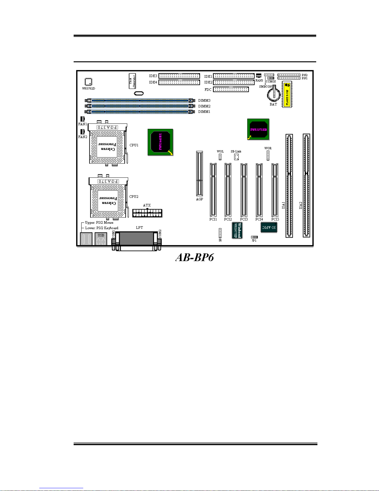
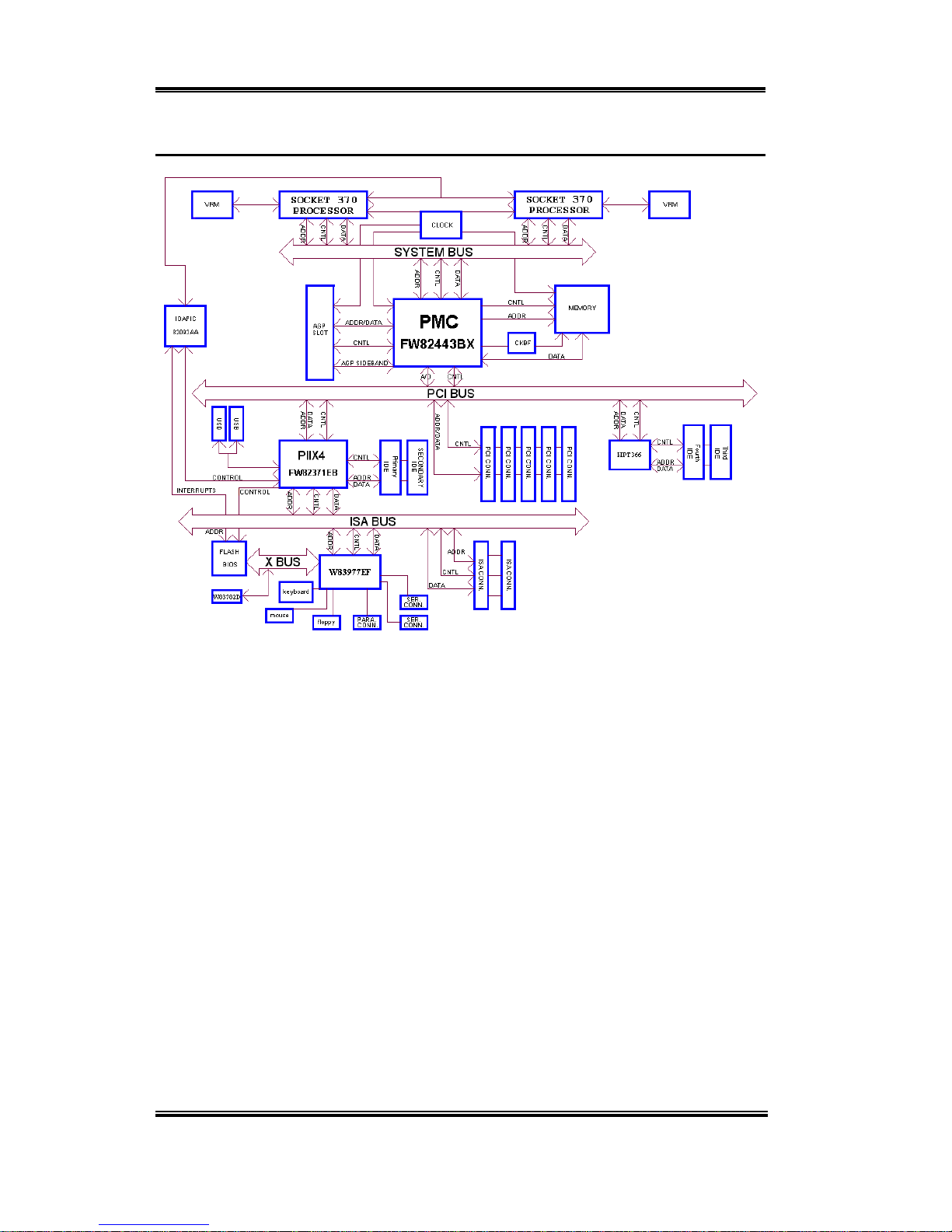
This motherboard is a specialdesign forSocket 370 CPUs. It is equipped withtwo PGA 370
sockets with which you can install two Socket 370 processors.
The BP6 has the HPT366 Ultra ATA/66 Chipset built-in. This means, the BP6 will support
Ultra ATA/66 IDE devices. Ultra ATA/66 is the new standard for IDE devices. It enhances
existing Ultra ATA/33 technology by increasing both performance and data integrity. This
new high-speed interface doubles the Ultra ATA/33 burst data transfer rate to 66.6
Mbytes/sec. The result is the maximum disc performance using the current PCI local bus
environment. Another benefit is, you can connect another four IDE devices in your system
either Ultra ATA/33 IDE devices or Ultra ATA/66 IDE devices. You will have more
flexibility to expand your computer system.
The BP6 has built-in hardware monitoring functions (you can refer to Appendix C for
detailed information), they can monitor and protect your computer insuring a safe
computing environment. The BP6 also supports both the PS/2 keyboard and PS/2 mouse
wake up features (you can refer to section 3-8 for detailed information), letting you easily
wake up your system by these devices. The motherboard can provide high performance for
workstations and meets the requirements for desktop systems for multimedia in the future.
Sets You Free From the Y2K Threat
The potential threat of Year 2000 (Y2K) problems are making everyone very nervous. The
Y2K issue applies to almost any device, firmware, or software that operates on or with year
based dates. This problem is caused by a design flaw in the Real Time Clock (RTC) unit.
The RTC only changes the last two digits of the year code, but not the century information.
As a result, when it comes to 12:00 AM January 1, 2000 the RTC will switch from
December 31 11:59 PM 1999 to 12:00 AM January 1 1900.
Y2K compliance deals with the date change over from 31 December 1999 to 1 January 2000,
and with recording and reporting of all dates from the RTC including leap year dates. This
motherboard is free from the Y2K problem because its BIOS are Y2K compliant.

1-2 Chapter1
BP6
Please Note
If the operating system or application software cannot handle Year 2000 dates, you will
still be facing the Y2K threat because it is not a hardware problem that relates to the
motherboard itself. According to Award BIOS, it’s BIOS source code released after 31
May 1995 complies with all known Y2K issues; however, it may still fail the 2000.exe
test. Award has modified its BIOS source code to accommodate the requirements of
2000.exe. Award BIOS source code issued later than 18 November 1996 passes the
NTSL 2000.exe test program.
1-2. Specifications
1. CPU
!Supports Dual Socket 370 processors
!Supports Intel®Celeron™ 300A~466MHz processors (Based on 66MHz PPGA package)
2. Chipset
!Intel440BX (66/100MHz) AGPset
!HPT366 Ultra DMA/66 IDE controller supports Four Ultra DMA66 devices
!Supports Ultra DMA/33 IDE protocol
!Supports Advanced Configuration and Power Management Interface (ACPI)
!Supports AGP 1X/2X
3. Cache Memory
!Level 1 and Level 2 cache built into Intel®Celeron™processor (PPGA package)
4. Memory (System Memory)
!Three 168-pin DIMM sockets support SDRAM module
!Supports up to 768MB (8, 16, 32, 64, 128, 256MB SDRAM)
!ECC support
5. System BIOS
!CPU SOFT MENUTM II eliminates the need for jumpers or DIP switches needed to set
CPU parameters
!Award Plug and Play BIOS supports APM, DMI, and ACPI
!Write-Protect Anti-Virus function by AWARD BIOS
!Year 2000 Compliant

Introduction of BP6 Features 1-3
User’s Manual
6. Multi I/O Functions
!2x Channels of Bus Master IDE Ports supporting up to four Ultra DMA 33/66 devices
!2x Channels of Bus Master IDE Ports supporting up to four Ultra DMA 33 devices
!PS/2 Keyboard and PS/2 Mouse Connectors
!1x Floppy Port ( up to 2.88MB)
!1x Parallel Port (EPP/ECP)
!2x Serial Ports
!2x USB Connectors
7. Miscellaneous
!ATX form factor
!1 AGP slot, 5 PCI slots and 2 ISA slots
!Hardware monitoring – Included fan speed, voltages, System environment temperature
!Keyboard and PS/2 Mouse Power On
!Built-in Wake on LAN header
!Built-in IrDA TX/RX header
!Built-in SMBus connector
!Built-in Wake On Ring Header
!Board size: 305 ×240mm

1-4 Chapter1
BP6
"
""
"Supports Wake Up on LAN, Keyboard or Mouse, but your ATX power supply 5V
standby (5VSB) power must be able to provide at least a 720mA current capacity.
Otherwise, the functions may not work normally.
"
""
"PCI slots 4 and 5 use the same bus master control signal.
"
""
"PCI slot 3 shares IRQ signals with the HPT366 IDE controller (Ultra ATA/66). The
driver for the HPT 366 IDE controller supports IRQ sharing with other PCI
devices. But if you install a PCI card that doesn’t allow IRQ sharing with other
devices into PCI slot 3, you may encounter some problems. Furthermore, if your
Operating System doesn’t allow peripheral devices to share IRQ signals with each
other--Windows NT for example, you can’t install a PCI card into PCI slot 3.
"
""
"HPT 366 IDE controller is designed to support high-speed mass storage. Thus we
don’t suggest you connect non-disk devices that use ATA/ATAPI interfaces, such as
CD-ROM to HPT 366 IDE connector (IDE3&IDE4).
#Sound Blaster™is a registered trademark of Creative Technology Ltd. in the United
States and certain other countries. Sound Blaster-LINK™and SB-LINK™ are trademarks
of Creative Technology Ltd.
#Specifications and information contained in this manual are subject to change without
notice.
#All brand names and trademarks are the property of their respective owners.
Important Notice
Based on peripheral specifications and other considerations, the BP6 SMP (Symmetric
Multiple Processor) function is designed for testing only. The BP6 motherboard can’t
manage the SMP function alone. It must co-operate with the CPU and OS that support
the SMP function. Therefore, any damage caused by employing an improper or OS will
void the warranty.

Introduction of BP6 Features 1-5
User’s Manual
1-3. Layout Diagram
Figure 1-2. Motherboard component location

1-6 Chapter1
BP6
1-4. The System Block Diagram
Figure 1-3. The system diagram of BP6

Introduction of BP6 Features 1-7
User’s Manual
1-5. Dual Processor Knowledge You Should Know
The dual processor function of BP6 is a special design for Socket 370 CPUs. The BP6
supports Intel®SMP (Symmetric Multiple Processor) specs. It is equipped with two PGA
370 sockets with which you can install two Socket 370 processors. Of course, you can also
install only one Socket 370 processor if you like. A single Socket 370 processor can be
installed in either PGA 370 socket, and no specific boot processor socket needs to be
selected.
To install two Socket 370 processors, we strongly recommend you to use the same speed
CPUs. Otherwise, your system may not operating properly.
For best performance, you should use an OS (Operating System) that supports multi-
processors. The following OSes can support multi-processor functions: Microsoft
WindowsNT (3.5x, 4.x and 5.x), SCO Unix, FreeBSD 3.0 or later, Linux, etc.
Of course, you can use Microsoft Windows3.1, Windows95 or Windows98 but they do
not support the SMP specs, therefore; using two processors will yield the same result as
using a single processor.
Important Notice
!Based on peripheral specifications and other considerations, the BP6 SMP
(Symmetric Multiple Processor) function is designed for testing only. The BP6
motherboard can’t manage the SMP function alone. It must co-operate with the CPU
and OS that support the SMP function. Therefore, any damage caused by employing
an improper or OS will void the warranty.
!If you only want to install one socket 370 CPU we suggest you use the CPU1 socket.

1-8 Chapter1
BP6

Installing the Motherboard 2-1
User’s Manual
Chapter 2 Installing the Motherboard
The BP6 motherboard not only provides all of the standard equipment for personal
computers, but also provides great flexibility for meeting future upgrade demands. This
chapter will introduce, step by step, all the standard equipment and will also present, as
completely as possible, future upgrade capabilities. This motherboard is able to support all
IntelCeleron™PPGA processors now on the market. (For details, see specifications in
Chapter 1.)
This chapter is organized according to the following features:
2-1 Installing the Motherboard to the Chassis
2-2 Installation of the Socket 370 processor
2-3 Installing System Memory
2-4 Connectors, Headers and Switches
$$$$
$$$$$$$$
$$$$ Before Proceeding with the Installation $$$$
$$$$$$$$
$$$$
Before you install or unplug any connectors or add-on cards, please remember to turn the
ATX power supply switch off (fully turn the +5V standby power off), or take the power cord
off. Otherwise, you may cause the motherboard components or add-on cards to malfunction
or be damaged.
%
%%
%
User Friendly Instructions
Our objective is to enable the novice computer user to perform the installation by himself.
We have attempted to write this document in a very clear, concise and descriptive manner to
help overcome any obstacles you may face during installation. Please read our instructions
carefully and follow them step-by-step.

2-2 Chapter2
BP6
2-1. Installing the Motherboard to the Chassis
Most computer chassis will have a base on which there will be many mounting holes that
allows the motherboard to be securely attached and at the same time, prevents short circuits.
There are two ways to attach the motherboard to the base of chassis:
!with studs
!or with spacers
Please refer to the figure 2-1 that shows the studs and spacers, they may have several types,
but all look like the figures below:
In principle, the best way to attach the
motherboard is with studs, and only if
you are unable to do this should you
attach the board with spacers. Take a
careful look at the motherboard and
you will see many mounting holes on
it. Line these holes up with the
mounting holes on the base. If the
holes line up, and there are screwholes
this means you can attach the motherboard with studs. If the holes line up and there are only
slots, this means you can only attach the motherboard with spacers. Take the tip of the
spacers and insert them into the slots. After doing this to all the slots, you can slide the
motherboard into position aligned with the slots. After the motherboard has been positioned,
check to make sure everything is OK before putting the casing back on.
Figure 2-2 shows you the way to affix the motherboard using studs or spacers:

Installing the Motherboard 2-3
User’s Manual
Note
If the motherboard has mounting holes, but they don’t line up with the holes on the base
and there are no slots to attach the spacers, don’t worry, you can still attach the spacers
to the mounting holes. Just cut the bottom portion of spacers (the spacer may be a little
hard to cut off, so be careful of your hands). In this way you can still attach the
motherboard to the base without worrying about short circuits. Sometimes you may
need to use the plastic springs to isolate the screw from the motherboard PCB surface,
because the circuit wire may be near by the hole. Be careful, don’t let the screw contact
any printed circuit wire or parts on the PCB that are near the fixing hole, otherwise it
may damage the board or cause board malfunctioning.
2-2. Installation of the Socket 370 processor
The Socket 370 processor installation is easy, like Pentium®processors before. Because it
uses the “Socket 370” ZIF (Zero Insertion Force) socket, it can easily let you fix the
processor on to its position firmly.
Figure 2-3 shows you what the 370 socket looks like, and how to open the lever. Its pin count
is more than socket 7. Therefore, the Pentium level processor cannot be inserted into socket
370.
When you raise the lever, you have loosened the socket
lock. Please raise the lever to the end, and prepare to
insert the processor. Next, you need to align the processor
pin 1 to socket pin 1. If you put it in the wrong direction,
you will not be able to insert the processor easily, and
processor pins will not fully go into the socket. If that is
the case, please change the direction, until it easily and
fully inserts into the 370 socket. See Figure 2-4.
When you finish the above, then push the lever down to
its original position, and you should feel the lever lock up
the 370 socket. You have then finished the processor
installation.

2-4 Chapter2
BP6
2-3. Installing System Memory
This motherboard provides three 168-pin DIMM sites for memory expansion. The DIMM
sockets support 1Mx64 (8MB), 2Mx64 (16MB), 4Mx64 (32MB), 8Mx64 (64MB), 16Mx64
(128MB), and 32Mx64 (256MB) or double sided DIMM modules. Minimum memory size
is 8MB and maximum memory size is 768MB SDRAM. There are three Memory module
sockets on the system board. (Total six banks)
In order to create a memory array, certain rules must be followed. The following set of rules
allows for optimum configurations.
!The memory array is 64 or 72 bits wide. (depending on with or without parity)
!Those modules can be populated in any order.
!Supports single and double density DIMMS.
Table 2-1. Valid Memory Configurations
Bank Memory Module Total Memory
Bank 0, 1
(DIMM1) 8MB, 16MB,32MB,
64MB, 128MB, 256MB 8MB ~ 256MB
Bank 2, 3
(DIMM2) 8MB, 16MB,32MB,
64MB, 128MB, 256MB 8MB ~ 256MB
Bank 4, 5
(DIMM3) 8MB, 16MB,32MB,
64MB, 128MB, 256MB 8MB ~ 256MB
Total System Memory 8MB ~ 768MB
Generally, installing SDRAM modules to your motherboard is an easy thing to do. You can
refer to figure 2-5 to see what a 168-pin PC100 SDRAM module looks like.
Unlike installing SIMMs,
DIMMs may be "snapped"
directly into the socket. Note:
Certain DIMM sockets have
minor physical differences. If
your module doesn't seem to
fit, please do not force it into
the socket as you may
damaged your memory module or DIMM socket.
The following procedure will show you how to install a DIMM module into a DIMM socket.
Step 1. Before you install the memory module, please place the computer power switch in
the off position and disconnect the AC power cord from your computer.

Installing the Motherboard 2-5
User’s Manual
Step 2. Remove the computer’s chassis cover.
Step 3. Before touching any
electronic components, make sure
you first touch an unpainted,
grounded metal object to discharge
any static electricity stored on your
clothing or body.
Step 4. Locate your computer’s
168-pin memory expansion DIMM
socket.
Step 5.Insert the DIMM module
into the expansion socket as shown
in the illustration. Note how the
module is keyed to the socket. You can refer to figure 2-6 for the details. This insures the
DIMM module will be plugged into the socket in one way only. Firmly press the DIMM
module into the DIMM socket, making certain the module is completely seated in the
DIMM socket.
Step 6. Once the DIMM module has been installed, the installation is complete and the
computer’s cover can be replaced. Or you can continue to install other devices and
add-on cards that are mentioned in the following section.
Note
When you install a DIMM module fully into the DIMM socket, the eject tab should be
locked into the DIMM module very firmly and fit into its indention on the both sides.

2-6 Chapter2
BP6
2-4. Connectors, Headers and Switches
Inside the case of every computer, several cables and plugs have to be connected. These
cables and plugs are usually connected one-by-one to connectors located on the
motherboard. You need to carefully pay attention to any connection orientation the cables
may have and, if any, noticethe position of the first pin of the connector. In the explanations
that follow, we will describe the significance of the first pin.
We will show you all connectors, headers and switches here, and tell you how to connect
them. Please pay attention and read the whole section for necessary information before
attempting to finish all of the hardware installation inside the computer chassis.
Figure 2-7 shows you all of the connectors and headers that we’ll discuss in the next section,
you can use this diagram to visually locate each connector and header we describe.
All connectors, headers and switches mentioned here, will depend on your system
configuration. Some features you may (or may not) have and need to connect or configure
depending on the peripheral. If your system doesn't have such add-on cards or switches you
can ignore some special feature connectors.
Figure 2-7. All Connectors and Headers for the BP6
First, Let’s see the headers that BP6 uses, and what their functions are.

Installing the Motherboard 2-7
User’s Manual
ATX: ATX Power Input Connector
Caution
If the power supply connectors are not properly attached to the ATX power supply, the
power supply or add-on cards may be damaged.
Attach the connector from the power supply
to the ATX connector here. Remember you
have to push the connector from the ATX
power supply firmly to the end with the
ATX connector, insuring that you have a
good connection.
Note: Watch the pin position and the
orientation
FAN 1/2/3: FAN Headers
Attach the connector from the individual
CPU1 fan to the header named FAN1, and
attach the CPU2 fan to the FAN2 header.
The FAN 3 speed can’t be monitored by the
system and can’t be turned off.
You must attach the CPU fan to the
processor, or your processor will work
abnormally or may be damaged by
overheating. Also, if you want the computer
case’s internal temperature to be kept steady
and not too high, you had better connect the chassis fan to reach this goal.
Note: Watch the pin position and the orientation

2-8 Chapter2
BP6
IR: IR Header (Infrared) There is a specific orientation for pins 1
through 5, attach the connector from the IR
KIT or IR device to the IR header. This
motherboard supports standard IR transfer
rates.
Note: Watch the pin position and the
orientation
SB-Link: SB-Link™Header If your PCI audio adapter supports this
feature, then you can connect the specific
cable from the audio adapter to this header.
SB-LINK™combines Intel's PC-PCI and
"Serialized IRQ" protocols. These
technologies can be found in Intel's TX, LX,
BX and newer core logic chipsets. This
technology provides the DMA and IRQ
signals present in ISA Bus today, but not
available on the PCI Bus. The SB-LINK™
serves as a bridge between the motherboard
and PCI sound card to deliver Sound card for real-mode DOS games. Check to see if your
card supports this.
Note: Watch the pin position and the orientation
WOR: Wake On Ring Header If you have an internal modem adapter that
supports this feature, then you can connect
the specific cable from the internal modem
adapter to this header. This feature lets you
wake up your computer via remote control
through the modem card.
Note: Watch the pin position and the
orientation
This manual suits for next models
1
Table of contents
Other Abit Motherboard manuals