Acer AL501 User manual

1
1.ELECTRICAL REQUIREMENTS.................................................................................... 2
A. LCD Panel Specification............................................................................................................................2
B. Controls.....................................................................................................................................................3
C. Power Management ..................................................................................................................................3
D.Display Modes FOR Inspections...............................................................................................................5
2.ADJUSTMENT CONDITIONS......................................................................................... 6
A. Measuring Apparatuses Used...................................................................................................................6
B. Input Signal................................................................................................................................................6
C.Indication ...................................................................................................................................................6
3.ADJUSTMENT OF POWER SUPPLY ...................................................................... 6
A. Adjustment of Switching Regulator (Adapter) ...........................................................................................6
4.ADJUSTMENT OF BOARDS.......................................................................................... 7
A. Connection Method ...................................................................................................................................7
5.VL-531 DISPLAY CONTROL BOARD............................................................................ 7
A. Description.................................................................................................................................................7
B. Features ....................................................................................................................................................7
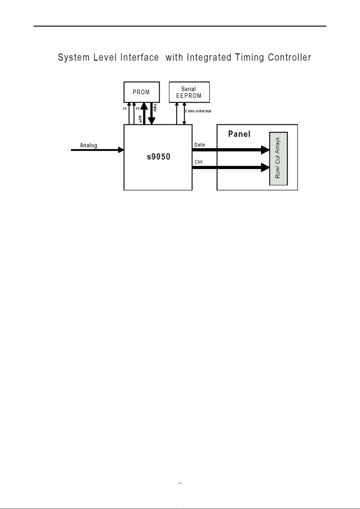
C.Block Diagram (Control Ckt)......................................................................................................................8
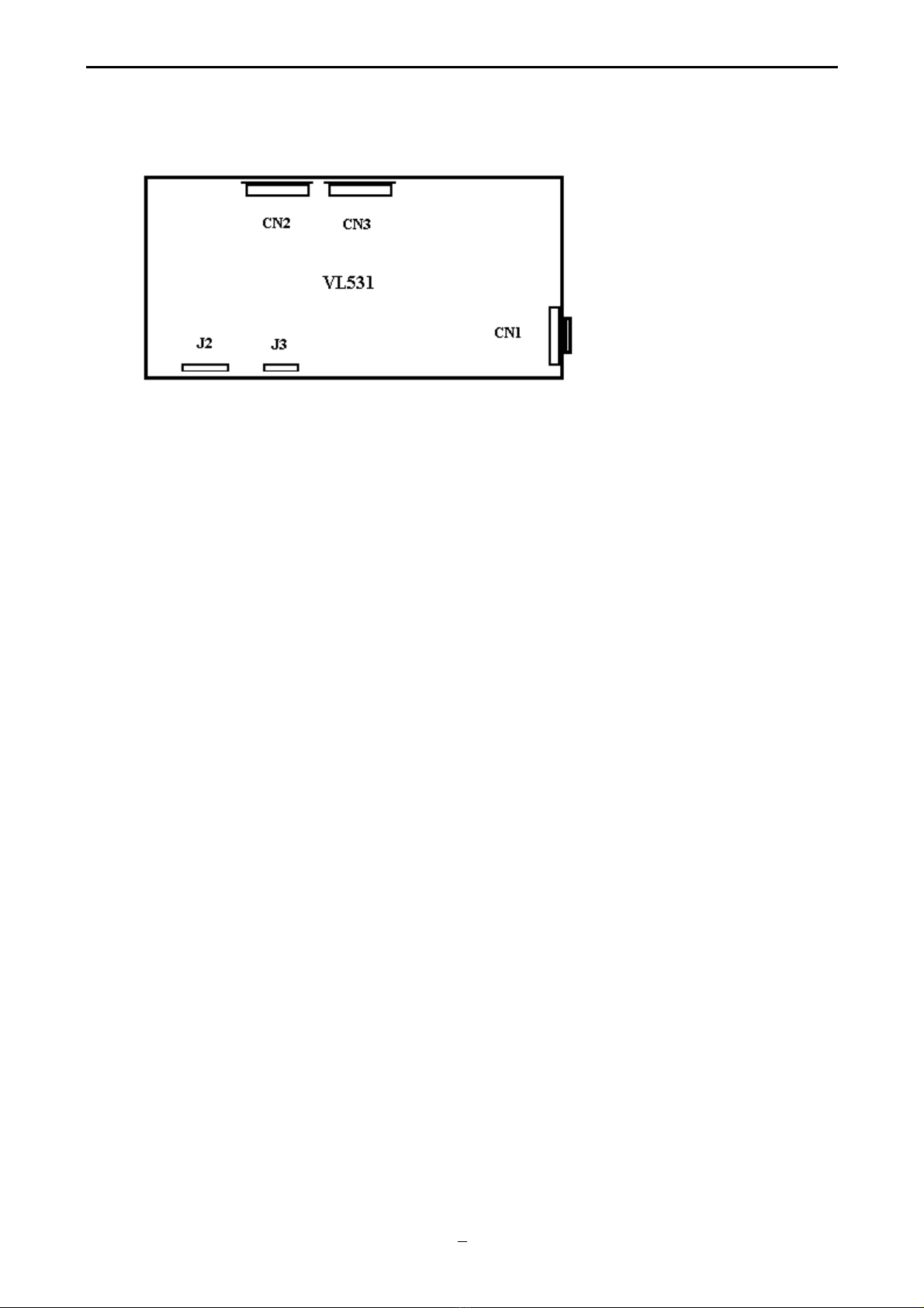
D.Connector Locations..................................................................................................................................9
E. Connector Type.........................................................................................................................................9
F. Connector Pin Assignment......................................................................................................................10
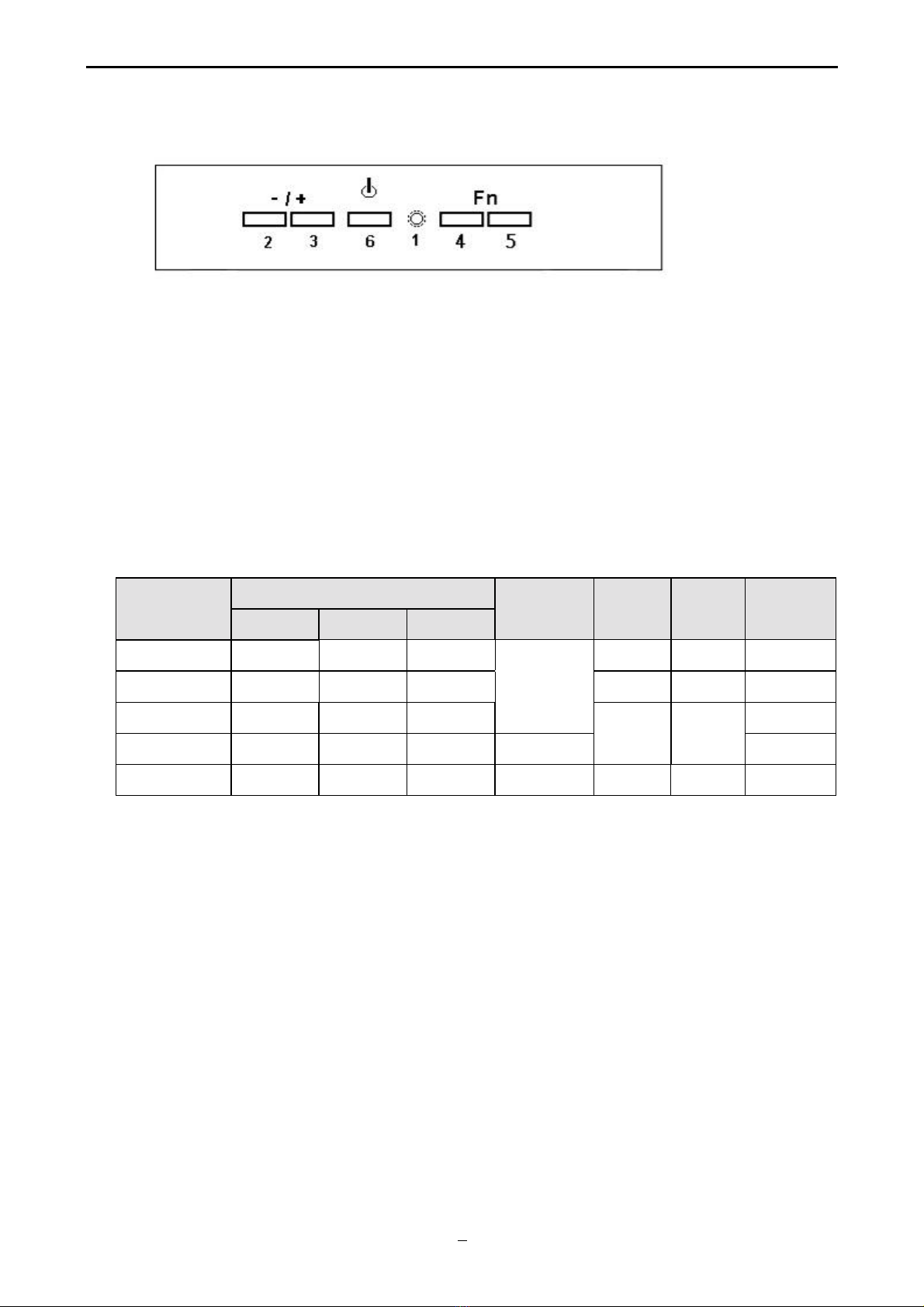
6.VK-531 CONTROL PANEL BOARD............................................................................. 14
A. Description...............................................................................................................................................14
B. Connector and Switch Locations.............................................................................................................14
C.Connector type........................................................................................................................................14
D.Connector pin Assignment......................................................................................................................15
7.VP-531 POWER BOARD.............................................................................................. 17
A. Description...............................................................................................................................................17
B. Electrical characteristics..........................................................................................................................17
C.Connector locations.................................................................................................................................18
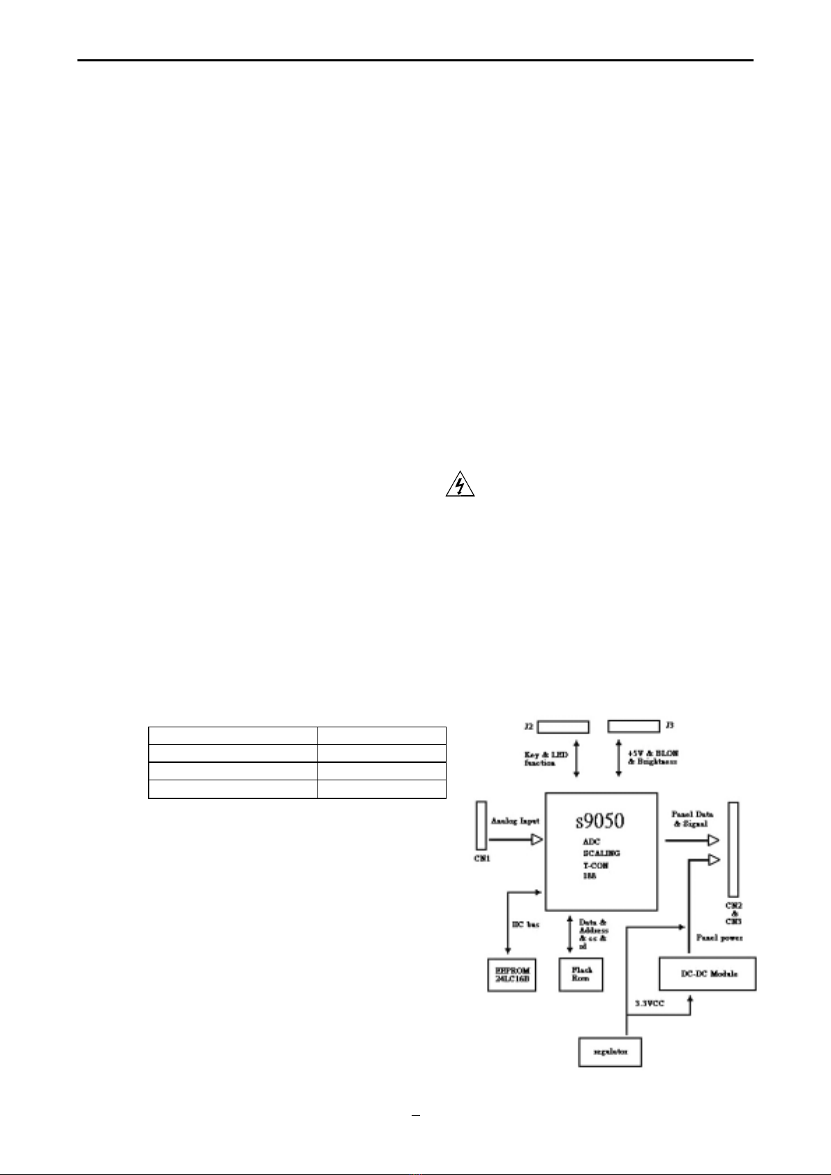
8.CIRCUIT DESCRPTION ............................................................................................... 20
A. Micro-Controller Circuit............................................................................................................................20
B. Circuit of Plug and Play...........................................................................................................................20
C.System Clock...........................................................................................................................................20
D.Image Engine (Zoom)..............................................................................................................................20
E. Power Regulator......................................................................................................................................20
9.INTRODUCTION........................................................................................................... 21
A. Front Panel Control And Led...................................................................................................................21
B. Rear Panel Connector Input Signals.......................................................................................................22
10.TROUBLESHOOTING................................................................................................. 23
A. Main Procedure.......................................................................................................................................23
APPENDIX A: PARATS LISTS……………..…………………………………………………..28
APPENDIX B: DISPLAY UNIT ASSEMBLY…………………………………………………..35
APPENDIX C: P.C.B.A ASSEMBLY…………………………………………………………...40

2
1. ELECTRICAL REQUIREMENTS
A. LCD Panel Specification
Display: 15 inch (15” viewable image size): active matrix: thin film transistor
(TFT): liquid crystal display (LCD): 0.297 mm dot pitch: R.G.B.
Vertical stripe 200 cd//m2 white luminance, typical: 300:1 contrast
ratio, typical
Compatibility: 640 x 350: VGA-350
720 x 400: VGA text
640 x 400: VGA-GRAPH
640 x 480: VGA, 60Hz to 75 Hz vertical refresh rate
800 x 600: 56Hz to 75 Hz vertical refresh rate
1024 x 768 non-interlaced: 60Hz to 75 Hz vertical refresh rate
Synchronization
Frequencies: Horizontal: 24 kHz to 60 kHz
Vertical: 56 Hz to 75 Hz (1024 x 768 is up to 75 Hz)
Pixel Frequency: 21 Mhz to 78 Mhz
Resolution: Horizontal: 1024 dots
Vertical: 768 lines
Active Display Area: Horizontal: 304.1 mm
Vertical: 228.1 mm
Viewing Angles: Up 40deg down 45deg (TYP)
Left 60deg, Right 60deg (TYP)
CR > 10
Display Colors: 6-bits driver
Power Supply: AC 100 to 240V worldwide input, 50 / 60Hz
Power
Consumption: Typical: 25W on mode +10 / -25%
Environmental: Operating temperature: 0ºC to 50ºC
Storage temperature: -20ºC to 65ºC
Storage humidity: 10%~90%

3
B. CONTROLS
B-1 Control panel (monitor front panel)
1. Power LED, ( Please refer to C-2 LED definition table)
2. Adjust decrease.
3. Adjust increase
4. Function select counter-clockwise.
5. Function select clockwise.
6. Power ON/OFF switch, push to ON and push to OFF. (toggle switch)
C. Power Management
C-1 Power Management condition and status
State Signals Power Video LCD LED
Horizontal Vertical Video Supply Circuit
On Pulses Pulses Active On On On Green
Stand-by No Pulses Pulses Blanking Off Off Yellow
Suspend Pulses No Pulses
Off No pulses No pulses Blacking On Yellow
DC Power off Don’t care Don’t care Don’t care Off Off Off Off

4
C-2 LED definition Table
State LED
On mode Green
Stand-by Yellow
Suspend Yellow
Off mode Yellow
DC power off Dark
disconnection 1. Yellow(stand-by; suspend; off mode)
2. LED Dark (DC power off)
C-3 Power Consumption
Meet VESA DPMS Proposal
On mode 25 Wmax
Stand-by 5 Wmax
Suspend 5 Wmax
Off mode 5 Wmax
DC power off 5 Wmax
disconnection 5 Wmax
Measured from AC input end of AC power adapter, and not include audio at power-saving state
The stand-by, suspend and off mode recover to on mode about 3 seconds.

5
D. Display Modes FOR Inspections
D-1 Supported Timing(for Not supported timing will go to power saving mode)T
TIMING FH(KHZ)
FV(HZ)
SYNC
POLARITY
TOTAL
(DOT/LINE)
ACTIVE
(DOT/LINE)
SYNC
WIDTH
(DOT/LINE)
FRONT
PORCH
(DOT/LINE)
BACK
PORCH
(DOT/LINE)
PIXEL
FOREQ.
(MHZ)
31.469 +800 640 96 16 48 25.175
640x350
VGA-350 70.087 −449 350 2 37 60
24.83 −848 640 64 64 80 21.05
640x400
NEC PC9801 56.42 −440 400 8 7 25
31.469 −800 640 96 16 48 25.175
640x400
VGA-GRAPH 70.087 +449 400 2 12 35
31.5 −800 640 64 16 80 25.197
640x400
NEC PC9821 70.15 −449 400 2 13 34
31.469 −800 640 96 16 48 25.175
640x480
VGA-480 59.94 −525 480 2 10 33
37.861 −832 640 40 16 120 31.5
640x480
VESA-480-72Hz 72.809 −520 480 3 1 20
37.5 −840 640 64 16 120 31.5
640x480
VESA-480-75Hz 75 −500 480 3 1 16
31.469 −900 720 108 18 54 28.322
720x400
VGA-400-TEXT 70.087 +449 400 2 12 35
35.156 +1024 800 72 24 128 36
800x600
SVGA 56.25 +625 600 2 1 22
37.879 +1056 800 128 40 88 40
800x600
VESA-600-60Hz 60.317 +628 600 4 1 23
48.077 +1040 800 120 56 64 50
800x600
VESA-600-72Hz 72.188 +666 600 6 37 23
46.875 +1056 800 80 16 160 49.5
800x600
VESA-600-75Hz 75 +625 600 3 1 21
49.725 - 1152 832 64 32 224 57.2832
832x624
APPLE MAC-800 74.55 - 667 624 3 1 39
48.363 −1344 1024 136 24 160 65
1024x768
XGA 60.004 −806 768 6 3 29
53.964 +1328 1024 176 16 112 71.664
1024x768
COMPAQ-XGA 66.132 +816 768 4 8 36
56.476 −1328 1024 136 24 144 75
1024x768
VESA-768-70Hz 70.069 −806 768 6 3 29
60.023 +1312 1024 96 16 176 78.75
1024x768
VESA-768-75Hz 75.029 +800 768 3 1 28

6
2. ADJUSTMENT CONDITIONS
A. Measuring Apparatuses Used
Necessary measuring equipment that for the adjustment of LA-1221JMW’s MAIN PWB are
following items.
Adjusted Video Generator.
Oscilloscope (more than 4 channels required)
DC voltmeter
B. Input Signal
Input signal by using video signal generator with VGA Card port for this adjustment.
C. Indication
Input signal by using video signal generator with VGA Card port for this adjustment.
3. ADJUSTMENT of Power Supply
A. Adjustment of Switching Regulator (Adapter)
A-1 Specifications
Input voltage AC 100 ~ 240Vac
Rated input voltage AC 90 ~ 264Vac
Frequency 50 / 60 Hz
Rated frequency 47 ~ 63 Hz
DC output
Out voltage +12V
Maximum output current 3.33A
Minimum output current 0A
Range of voltage Regulation ±5%

7
4. ADJUSTMENT OF BOARDS
Equipment is connected with boards to be inspected before adjustments. Refer to diagram
below.
A. Connection Method
1. R.G.B Signal Cable
2. DC Power Cable
3. Inverter Cable
4. Control Cable
5. LCD Lamp Cable
5. VL-531 DISPLAY CONTROL BOARD
A. Description
The VL-531 display control board is design to directly convert the R.G.B signals from VGA
Card D-sub port to optimum LCD timing signals so as to construct a high display quality LCD
monitor.
B. Features
• On board sage chip to detect display timings and control user functions.
• Using sage chip to convert R.G.B signals to digital timing
• Using sage chip to offer full screen expansion function on non-XGA mode(Auto-Zoom).
• Support VESA DPMS function.
• Support DDC2B functions.

8
C. Block Diagram (Control CKT)
C-1 Sage Operation
The s9050-100 is highly-integrated display processors. It has an ADC/PLL block and a
microprocessor integrated on a single chip. The cost-effective s9050-100 is suitable for the
XGA and the s9050 for the SXGA market segment with smaller memory requirements. Other
features include a brand new high-end scaler, Active Color Management, a flexible OSD,
Autoadjust, SureSyncTM and independent monitoring of the analog interface. A new standalone
on-chip pattern generator has been incorporated to simplify the manufacture of monitors.

9
D. Connector Locations
E. Connector Type
Location Type Maker Number of pins
CN1 DZ11A91-L8 P1.524 FEMALE 15
J2 96113-1003 E&T 10
J3 96113-0703 E&T 7
CN3 98210-4011 E&T 40
CN2 98210-4011 E&T 40

10
F. Connector pin assignment
F-1 CN1
Pin NO. Signal Comment
1 R-Video Red Video Input.
2 G-Video Green Video Input.
3 B-Video Blue Video Input.
4 Ground Ground
5 Ground Ground
6 Ground Ground.
7 Ground Ground.
8 Ground Ground
9 5V-DCC DDC Power Input.
10 NC NC
11 Ground Ground
12 DDC-SDA DDC 2B Data
13 HS Horizontal Sync Input.
14 VS Vertical Sync Input.
15 DDC-SCL DDC 2B Clock

11
F-2 CN3
Terminal No. Symbol Function
1 VDD1 Digital Power Input (DC+3.3V)
2 VDD1 Digital Power Input (DC+3.3V)
3 GND Ground
4 GND Ground
5 0B5 Odd-dot Blue Data bit 5 (MSB)
6 0B4 Odd-dot Blue Data bit 4
7 0B3 Odd-dot Blue Data bit 3
8 0B2 Odd-dot Blue Data bit 2
9 0B1 Odd-dot Blue Data bit 1
10 0B0 Odd-dot Blue Data bit 0
11 GND Ground
12 0G5 Odd-dot Green Data bit 5 (MSB)
13 0G4 Odd-dot Green Data bit 4
14 0G3 Odd-dot Green Data bit 3
15 0G2 Odd-dot Green Data bit 2
16 0G1 Odd-dot Green Data bit 1
17 0G0 Odd-dot Green Data bit 0 (LSB)
18 GND Ground
19 0R5 Odd-dot Red Data bit 5 (MSB)
20 0R4 Odd-dot Red Data bit 4
21 0R3 Odd-dot Red Data bit 3
22 0R2 Odd-dot Red Data bit 2
23 0R1 Odd-dot Red Data bit 1
24 0R0 Odd-dot Red Data bit 0 (LSB)
25 GND Ground
26 CPH2 Pixel Clock Input
27 GND Ground
28 GND Ground
29 NC No connecting
30 NC No connecting
31 VGH Gate Driver High Voltage Input
32 NC No connecting
33 VGL Gate Driver Low Voltage Input
34 NC No connecting
35 VGC Gate Driver Common Voltage Input
36 NC No connecting
37 NC No connecting
38 NC No connecting
39 GND Ground
40 GND Ground

12
F-3 CN2
Terminal No. Symbol Function Terminal No. Symbol Function
1 VDD2 Analog Power Input (DC+9V) 31 POL Source Driver Output
Polarity Control
2 VDD2 Analog Power Input (DC+9V) 32 REV Data Reverse Control
Signal
3 GND Ground 33 GND Ground
4 GND Ground 34 GND Ground
5 EB5 Even-dot Blue Data bit 5(MSB) 35 STV1 Vertical start Pulse1
6 EB4 Even-dot Blue Data bit 4 36 STV2 Vertical start Pulse2
7 EB3 Even-dot Blue Data bit 3 37 CPV Vertical Clock Input
8 EB2 Even-dot Blue Data bit 2 38 OE Gate Driver Output Enable
Signal
9 EB1 Even-dot Blue Data bit 1 39 GND Ground
10 EB0 Even-dot Blue Data bit 0 (LSB) 40 GND Ground
11 GND Ground
12 EG5 Even-dot Green Data bit 5 (MSB)
13 EG4 Even-dot Green Data bit 4
14 EG3 Even-dot Green Data bit 3
15 EG2 Even-dot Green Data bit 2
16 EG1 Even-dot Green Data bit 1
17 EG0 Even-dot Green Data bit 0 (LSB)
18 GND Ground
19 ER5 Even-dot Red Data bit 5 (MSB)
20 ER4 Even-dot Red Data bit 4
21 ER3 Even-dot Red Data bit 3
22 ER2 Even-dot Red Data bit 2
23 ER1 Even-dot Red Data bit 1
24 ER0 Even-dot Red Data bit 0 (LSB)
25 GND Ground
26 CPH1 Pixel Clock Input
27 GND Ground
28 GND Ground
29 STH Horizontal start Pulse
30 LOAD Source Driver Latch Pulse

13
F-4 J2
Pin NO. Signal Comment
1 NONE
2 LED-Y Power saving mode
3 LED-G Monitor is ON
4 GND GND
5 KEY-UP Function select counter-clockwise key
6 KEY-Down Function select counter-clockwise key
7 KEY-R Adjust up key
8 KEY-L Adjust down key
9 KEY-POWER Power ON/OFF key
10 GND GND
F-5 J3
Pin NO. Signal Comment
1 +5V VL531 power input
2 +5V VL531 power input
3 GND Ground
4 GND Ground
5 BLON Back Light ON/OFF.
6 MUTE Audio amplifier control signal (No use)
7 BRIGHT Brightness Adjustment.

14
6. VK-531 Control Panel Board
A. Description
The VK-531 is designed to offer an user interfaced control panel which passes and
receives signals to and from VP-531 power board .
B. Connector and Switch Locations
C. Connector type
Location Type Maker Number of pins
J5 96113-1013 E&T 10

15
D. Connector pin Assignment
D-1 J5
Pin NO. Signal Comment
1 NONE
2 LED-Y Power saving mode.
3 LED-G Monitor on mode.
4,10 GND Ground
5 KEY-UP Function select up to VL-531
6 KEY-DOWN Function select down to VL-531
7 KEY-R Function select right to VL-531
8 KEY-L Function select left to VL-531
9 KEY-PWR Power ON/OFF signal to VL-531

16
D-2 Switch definition
Location Definition
S1 Power ON/OFF
S2 Function select by clockwise direction
S3 Function select by counter-clockwise direction
S4 Adjust up
S5 Adjust down
D-3 LED definition
Location Definition
D1 Green for ON mode; Yellow for DC power off; stand by;
suspend and off mode.

17
7. VP-531 POWER BOARD
A. Description
The VP-531 power board is designed for lighting up the back-lights of LCD module.
B. Electrical characteristics
B-1 FOR HANNSTAR PANEL
MIN. TYP. MAX. COMMENT
INPUT VOLTAGE 11.4V 12V 12.6V
INPUT CURRENT -------- 0.85A 1A Vin=12V MAX.
BRIGHTNESS
NO LOAD BACKLIGHT
VOLTAGE -------- 640V rms. --------
LAMP CURRENT 3mA rms. 6mA rms. 7mArms
DRIVING FREQUENCY 40KHz 55KHz 70KHz
EFFICIENCY -------- 75% -------- Vin = 12V
Operating Life Time 50,000 ------- -------- Hours (noto)
Note:
Life time(Hr) can be defined as the time in which it continues to operate under the
condition:
Ta=25±3°C, IL=6.0Ma(ms) and fL=30 KHz until one of the following event occurs:
1. When the brightness becomes 50%
2. When the startup voltage (Vs) at 0°C becomes higher than the maximal value of
Vs specified above
B-2 DC/DC power
B.2.1 Input
12V
B.2.2 Output
Item Output voltage max. load Min. load tolerence ripple & noise(max.)
Vcc 5V 1.2A 0.1A 150Vpp
B.2.3 Efficiency:78% typ. at maximum load.

18
C. Connector locations
C-1 Connector type VP-531
Location Type Maker Number of pins
J920,J960 SM02 (8.0)B-BHS-1 JST 2
J3 96113-0702 E&T 7
J801 SCD-014-I SC 2

19
C-2 Connector pin assignment
C.2.1 J920 & J960 VP-531
Pin NO. Signal Comment
1 LV Low voltage (common)
2 HV High voltage for lamp
C.2.2 J3
Pin NO. Signal Comment
1,2 Vcc +5V
5 Ven Back-light ON/OFF control , high active(3.3V)
3,4 GND
6 MUTE1 Audio mute (No use)
7 Vbr: BRITE Brightness (0-3.4V) control from VL-531
0.7V for min. brightness
C.2.3 J801 DC 12V INPUT
Pin No. Signal Comment
PIN1 +12V From adapter output cable
PIN2 GND From adapter output cable

20
8. CIRCUIT DESCRPTION
A. Micro-Controller Circuit
The U5 (s9050-100) is a system controller.
The Y1 is 14.318MHz XTAL.
B. Circuit of Plug and Play
Plug and play allows the serial communication of host PC and peripherals offering minimal
configurations to end users. This monitor supports DDC2B communication protocal.
SDATA and VCLK are input to U4 (24LC21A).
C. System Clock
The Y1 (14.318MHz XTAL) supports U5 (Sage) reference clock.
D. Image Engine (Zoom)
The U5 (Sage) is a image engine that have following functions.
(1) The Sage is a IFM ( Input Format Measurement )
(2) The Sage are both high guilty scalar and timing controller chip.
E. Power Regulator
(1)The U12(APL117) is 1A linear regulator that transfer input voltage from 5V to 3.3V
supports U5.
(2)The U13(AIC1084) is 5A linear regulator that transfer voltage from 5V to 3.3V supports
U17 and Panel Vcc.
(3)The U14 (APL1117) is 1A linear regulator that transfer voltage from 5V to 2.5V.
(4)The U15 (APL1117) is 1A linear regulator that transfer voltage from 5V to 2.5V.
Other manuals for AL501
1
Table of contents
Other Acer Monitor manuals