ADL ADLQM67PC User manual

ADL Embedded Solutions GmbH, Eiserfelder Str. 316, ADL Embedded Solutions Inc. 4411 Morena Blvd., Suite 101
57080 Siegen, Germany San Diego, CA 92117-4345
P. +49 (0) 271 250 810 0 F. +49 (0) 271 250 810 20 P. +1 858 490-0597 F. +1 858 490-0599
e-mail: sales@adl-europe.com; web: http://www.adl-europe.com e-mail: sales@adl-usa.com; web: http://www.adl-usa.com
ADLQM67PC
Manual
rev. 1.4


Contents
ADL Embedded Solutions ADLQM67PC page 3
Contents
0Document History................................................................................................................................. 6
1Introduction .......................................................................................................................................... 7
1.1 Important Notes ............................................................................................................................ 7
1.2 Technical Support......................................................................................................................... 7
1.3 Warranty ....................................................................................................................................... 7
1.4 Return Authorization..................................................................................................................... 7
1.5 Description of Safety Symbols...................................................................................................... 8
1.6 RoHS ............................................................................................................................................ 8
1.7 FCC Approvals for the United States of America......................................................................... 8
1.8 FCC Approval for Canada ............................................................................................................ 8
2Overview.............................................................................................................................................. 9
2.1 Features........................................................................................................................................ 9
2.2 Specifications and Documents ................................................................................................... 11
3Connectors......................................................................................................................................... 13
3.1 Connector Map ........................................................................................................................... 14
3.2 Power Supply.............................................................................................................................. 15
3.3 System/SM-Bus.......................................................................................................................... 16
3.4 Memory....................................................................................................................................... 17
3.5 PCIe/104 Connector ................................................................................................................... 20
3.6 DVI/HDMI.................................................................................................................................... 22
3.7 DisplayPort.................................................................................................................................. 23
3.8 VGA ............................................................................................................................................ 24
3.9 LCD............................................................................................................................................. 25
3.10 USB............................................................................................................................................. 27
3.11 LAN............................................................................................................................................. 28
3.12 Audio........................................................................................................................................... 29
3.13 SATA Interfaces.......................................................................................................................... 30
3.14 COM1 and COM2....................................................................................................................... 31
3.15 GPIO........................................................................................................................................... 32
3.16 Monitoring Functions .................................................................................................................. 33
4State LEDs......................................................................................................................................... 34
4.1 HD LED....................................................................................................................................... 34
4.2 RGB LED.................................................................................................................................... 35
5BIOS Settings..................................................................................................................................... 36
5.1 General Remarks........................................................................................................................ 36
5.2 Main............................................................................................................................................ 37
5.3 Advanced.................................................................................................................................... 39
5.3.1 PCI Subsystem Settings..................................................................................................... 41
5.3.2 ACPI Settings...................................................................................................................... 43
5.3.3 CPU Configuration.............................................................................................................. 44
5.3.4 SATA Configuration............................................................................................................ 46
5.3.5 Power Controller Options.................................................................................................... 47
5.3.6 USB Configuration.............................................................................................................. 49
5.3.7 Super IO Configuration....................................................................................................... 50
5.3.8 H/W Monitor........................................................................................................................ 52
5.3.9 Serial Port Console Redirection.......................................................................................... 54

Contents
page 4 ADL Embedded Solutions ADLQM67PC
5.3.10 Network Stack..................................................................................................................... 56
5.3.11 CPU PPM Configuration..................................................................................................... 57
5.3.12 Intel(R) GigabitNetworkConnection.................................................................................... 58
5.4 Chipset........................................................................................................................................ 60
5.4.1 PCH-IO Configuration......................................................................................................... 61
5.4.2 System Agent (SA) Configuration....................................................................................... 68
5.5 Boot............................................................................................................................................. 76
5.5.1 CSM Parameters ................................................................................................................ 78
5.6 Security....................................................................................................................................... 79
5.6.1 Secure Boot Policy ............................................................................................................. 80
5.6.2 Key Management................................................................................................................ 81
5.7 Save & Exit ................................................................................................................................. 83
5.8 BIOS-Update .............................................................................................................................. 84
6Mechanical Drawings......................................................................................................................... 85
6.1 PCB: Mounting Holes ................................................................................................................. 85
6.2 PCB: Pin 1 Dimensions .............................................................................................................. 86
6.3 PCB: Heat Sink/Die Center......................................................................................................... 87
6.4 Heat Spreader: Chassis Mount................................................................................................... 88
7Technical Data................................................................................................................................... 89
7.1 Electrical Data............................................................................................................................. 89
7.2 Environmental Conditions........................................................................................................... 89
7.3 Thermal Specifications ............................................................................................................... 90
IAnnex: Post-Codes............................................................................................................................ 92
II Annex: Resources.............................................................................................................................. 93
IO Range................................................................................................................................................ 93
Memory Range....................................................................................................................................... 93
Interrupt.................................................................................................................................................. 93
PCI Devices............................................................................................................................................ 94
SMB Devices.......................................................................................................................................... 94

Important Notes Chapter: Document History
ADL Embedded Solutions ADLQM67PC page 5

Chapter: Document History Important Notes
page 6 ADL Embedded Solutions ADLQM67PC
0 Document History
Version
Changes
0.1
first pre-release
0.2
corrected RAM frequency; explained DP pin 11, minor changes
1.0
first complete version
1.1
updated BIOS settings
1.2
chapter 3.16: pinout pin 7 and 9 corrected
1.3
chapter 2.1: added CPU
1.4
chapter 1.7 / 1.8: added FCC Approval
NOTE
All company names, brand names, and product names referred to in this manual are registered or
unregistered trademarks of their respective holders and are, as such, protected by national and
international law.
Important Notes Chapter: Introduction
ADL Embedded Solutions ADLQM67PC page 7
1 Introduction
1.1 Important Notes
Please read this manual carefully before you begin installation of this hardware device. To avoid
Electrostatic Discharge (ESD) or transient voltage damage to the board, adhere to the following rules at all
times:
oYou must discharge your body from electricity before touching this board.
oTools you use must be discharged from electricity as well.
oPlease ensure that neither the board you want to install, nor the unit on which you want to install this
board, is energized before installation is completed.
oPlease do not touch any devices or components on the board.
CAUTION
As soon as the board is connected to a working power supply, touching the board may result in electrical
shock, even if the board has not been switched on yet. Please also note that the mounting holes for heat
sinks are connected to ground, so when using an externally AC powered device, a substantial ground plane
differential can occur if the external device's AC power supply or cable does not include an earth ground.
This could also result in electrical shock when touching the device and the heat sink simultaneously.
1.2 Technical Support
Technical support for this product can be obtained in the following ways:
oBy contacting our support staff at +1 858-490-0597 or +49 (0) 271 250 810 0
oBy contacting our staff via e-mail at support@adl-usa.com or support@adl-europe.com
oVia our website at www.adl-usa.com/support or www.adl-europe.com/support
1.3 Warranty
This product is warranted to be free of defects in workmanship and material. ADL Embedded Solutions' sole
obligation under this warranty is to provide replacement parts or repair services at no charge, except
shipping cost. Such defects which appear within 12 months of original shipment of ADL Embedded
Solutions will be covered, provided a written claim for service under warranty is received by ADL Embedded
Solutions no less then 30 days prior to the end of the warranty period of within 30 days of discovery of the
defect –whichever comes first. Warranty coverage is contingent upon proper handling and operation of the
product. Improper use such as unauthorized modifications or repair, operation outside of specified ratings,
or physical damage may void any service claims under warranty.
1.4 Return Authorization
All equipment returned to ADL Embedded Solutions for evaluation, repair, credit return, modification, or any
other reason must be accompanied by a Return Material Authorization (RMA) number. ADL Embedded
Solutions requires a completed RMA request form to be submitted in order to issue an RMA number. The
form can be found under the Support section at our website: www.adl-usa.com or www.adl-europe.com.
Submit the completed form to support@adl-usa.com or fax to +1 858-490-0599 for the USA office, or to
Germany. Following a review of the information provided, ADL Embedded Solutions will issue an RMA
number.

Chapter: Introduction Description of Safety Symbols
page 8 ADL Embedded Solutions ADLQM67PC
1.5 Description of Safety Symbols
The following safety symbols are used in this documentation. They are intended to alert the reader to the
associated safety instructions.
ACUTE RISK OF INJURY!
If you do not adhere to the safety advise next to this symbol, there is immediate danger to life and health of
individuals!
RISK OF INJURY!
If you do not adhere to the safety advise next to this symbol, there is danger to life and health of individuals!
HAZARD TO INDIVIDUALS,ENVIRONMENT,DEVICES,OR DATA!
If you do not adhere to the safety advise next to this symbol, there is obvious hazard to individuals, to
environment, to materials, or to data.
NOTE OR POINTER
This symbol indicates information that contributes to better understanding.
1.6 RoHS
The PCB and all components are RoHS compliant (RoHS = Restriction of Hazardous Substances
Directive). The soldering process is lead free.
1.7 FCC Approvals for the United States of America
FCC: Federal Communications Commission Radio Frequency Interference Statement
This equipment has been tested and found to comply with the limits for a Class A digital device, pursuant to
Part 15 of the FCC Rules. These limits are designed to provide reasonable protection against harmful
interference when the equipment is operated in a commercial environment. This equipment generates,
uses, and can radiate radio frequency energy and, if not installed and used in accordance with the
instruction manual, may cause harmful interference to radio communications. Operation of this equipment
in a residential area is likely to cause harmful interference in which case the user will be required to correct
the interference at his own expense.
1.8 FCC Approval for Canada
FCC: Canadian Notice
This equipment does not exceed the Class A limits for radiated emissions as described in the Radio
Interference Regulations of the Canadian Department of Communications.

Features Chapter: Overview
ADL Embedded Solutions ADLQM67PC page 9
2 Overview
2.1 Features
The ADLQM67PC is a highly complex computer motherboard in the PC/104™ form factor, complying with
the state-of-the-art "PCIe/104™" standard. It's based on Intel®'s 2nd Generation Core™ and Celeron®
CPUs (BGA, embedded) combined with the QM67 PCH. Modern DDR3 technology provides top-notch
memory performance, accomodating up to 4 GByte of RAM (DDR3-1066/1333/1600) via SO-DIMM204.
PCI-Express is available through the PCI/104-Express Type 1 connector, offering one x16 connection and
four x1 lanes for connecting all kinds of expansion cards in a PCIe/104™ stack-down fashion. For
connecting graphics devices, several interfaces are available: CRT, LVDS, HDMI, DisplayPort. Additional
interfaces include two serial ports, two Gigabit Ethernet interfaces (LAN), two SATA channels (up to 6Gb/s),
an audio interface (HDA 7.1), and ten USB channels. There are also 16 discrete programmable GPIO
signals available.
oProcessor Intel® Core™ i7-2715QE, i7-2655LE, i7-3517UE or Celeron® 827E
oChipset Intel® QM67 PCH
oSO-DIMM204 socket for one DDR3-1066/1333/1600 module of up to 4 GByte
oTwo serial interfaces COM1-2
oTwo LAN interfaces Ethernet 10/100/1000 (Base-T)
oTwo SATA channels (1.5/3/6 Gb/s)
oPS2 keyboard / mouse interface
oTen USB 2.0 interfaces (two on PCI104-Express connector)
oBIOS AMI® Aptio
oDisplayPort interface
oHDMI interface
ddd
PCIe/104 connector (type 1)
Intel® QM67 PCH
SMSC®
SCH3114
LPC
Intel®
82574L
SO-DIMM204
DDR3-1066/1333
(dual channel)
MEMORY
Power VCCCore; VTT;
DDRVTT, GFXVCC
1,05V; 1,5V; 1,8V; 3,3V
BIOS
MS
2x SATA
RealTek®
ALC889 MIC 1/2
7.1 Audio
AUX l/r
HDA Link
KB
LAN2
USB9-10
COM1-2
CRT
Intel®: Core™
i7-2715QE,
i7-2655LE,
i7-3517UE,
Celeron® 827E
FDI
1.5/3/6 Gb/s
SPDIF i/o
Intel®
82579L
4x
PCIe x1 PCIe (x1) Gen. 2
FAN 1-3
USB 2.0
DMI
DP/HDMI
DVI/HDMI
SPI
PCIe x16 PCIe (x16) / PEG Gen. 2/3
16x GPIO
SMBus
LAN1
LVDS
18/24/36/48
SMBus
RealTek®
ALC889
NXP®
PCA9535
USB1-8 USB 2.0

Chapter: Overview Features
page 10 ADL Embedded Solutions ADLQM67PC
oCRT connection
oLCD connection via LVDS 18/24bit (dual pixel)
oHDA compatible sound controller with SPDIF in and out
oRTC with external CMOS battery
oPCI-Express bus via PCI/104-Express connector (type 1, one x16, four x1 lanes)
o16x GPIO
o5V and 12V supply voltage
oSize: 96 mm x 90 (115.5) mm

Specifications and Documents Chapter: Overview
ADL Embedded Solutions ADLQM67PC page 11
2.2 Specifications and Documents
In making this manual and for further reading of technical documentation, the following documents,
specifications and web-pages were used and are recommended.
PC/104™ Specification
Version 2.5
www.pc104.org
PC/104-Plus™ Specification
Version 2.0
www.pc104.org
PCI/104-Express™ Specification
Version 2.0
www.pc104.org
PCI Specification
Version 2.3 and 3.0
www.pcisig.com
ACPI Specification
Version 3.0
www.acpi.info
ATA/ATAPI Specification
Version 7 Rev. 1
www.t13.org
USB Specifications
www.usb.org
SM-Bus Specification
Version 2.0
www.smbus.org
Intel® Chipset Description
Intel® 6 Series Chipset Datasheet
www.intel.com
Intel® Chip Description
2nd Generation Core™ Processor Family Datasheet
www.intel.com
SMSC® Chip Description
SCH3114 Datasheet
www.smsc.com
(NDA required)
Intel® Chip Description
82574L Datasheet
www.intel.com
Intel® Chip Description
82579L Datasheet
www.intel.com
Realtek® Chip Description
ALC885/889 Datasheet
www.realtek.com.tw
Chrontel® Chip Description
Chrontel 7318C Datasheet
www.chrontel.com

Chapter: Overview Specifications and Documents
page 12 ADL Embedded Solutions ADLQM67PC
American Megatrends®
Aptio™ Text Setup Environment (TSE) User Manual
www.ami.com
American Megatrends®
Aptio™ 4.x Status Codes
www.ami.com

Specifications and Documents Chapter: Connectors
ADL Embedded Solutions ADLQM67PC page 13
3 Connectors
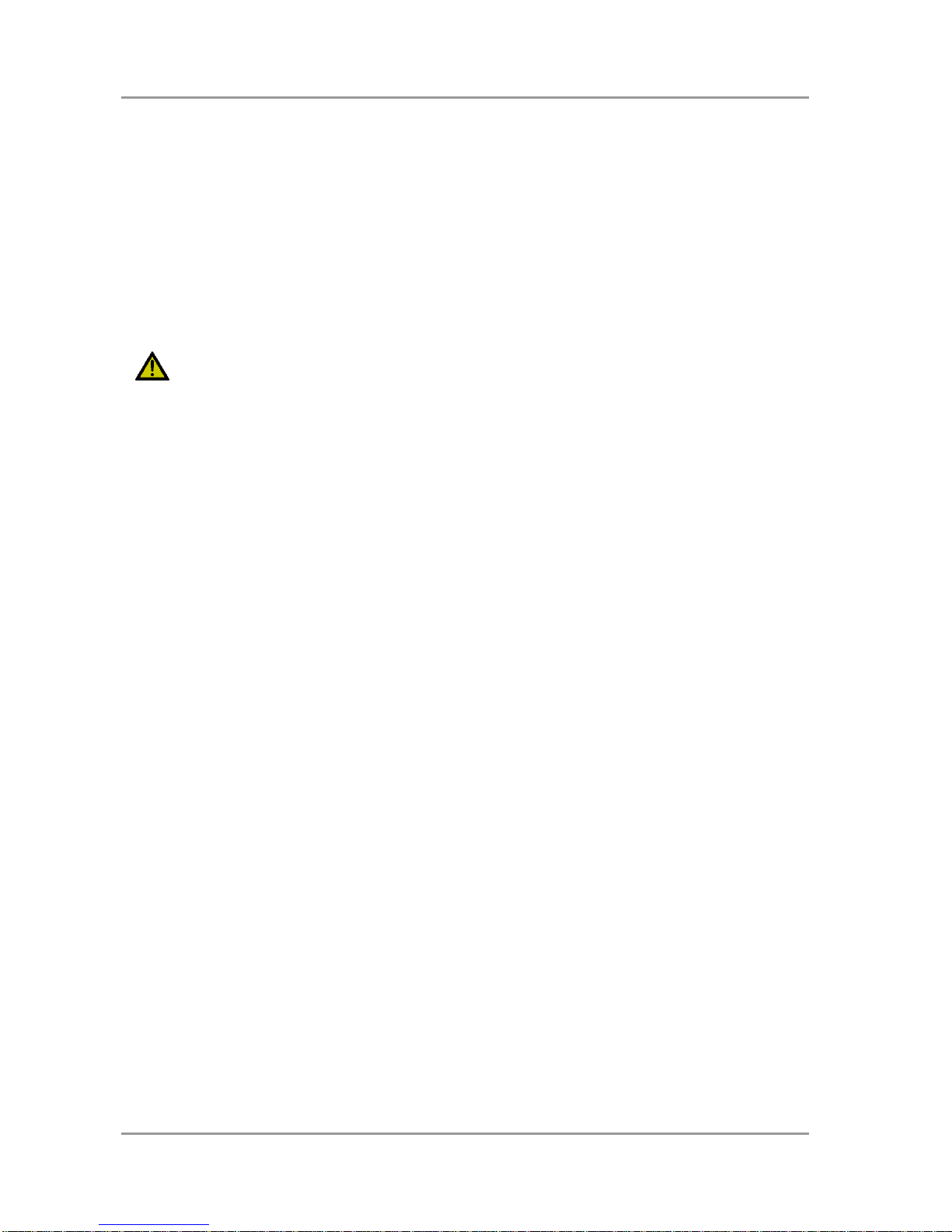
This section describes all the connectors found on the ADLQM67PC.
CAUTION
For most interfaces, the cables must meet certain requirements. For instance, USB 2.0 requires twisted and
shielded cables to reliably maintain full speed data rates. Restrictions on maximum cable length are also in
place for many high speed interfaces and for power supply. Please refer to the respective specifications and
use suitable cables at all times.
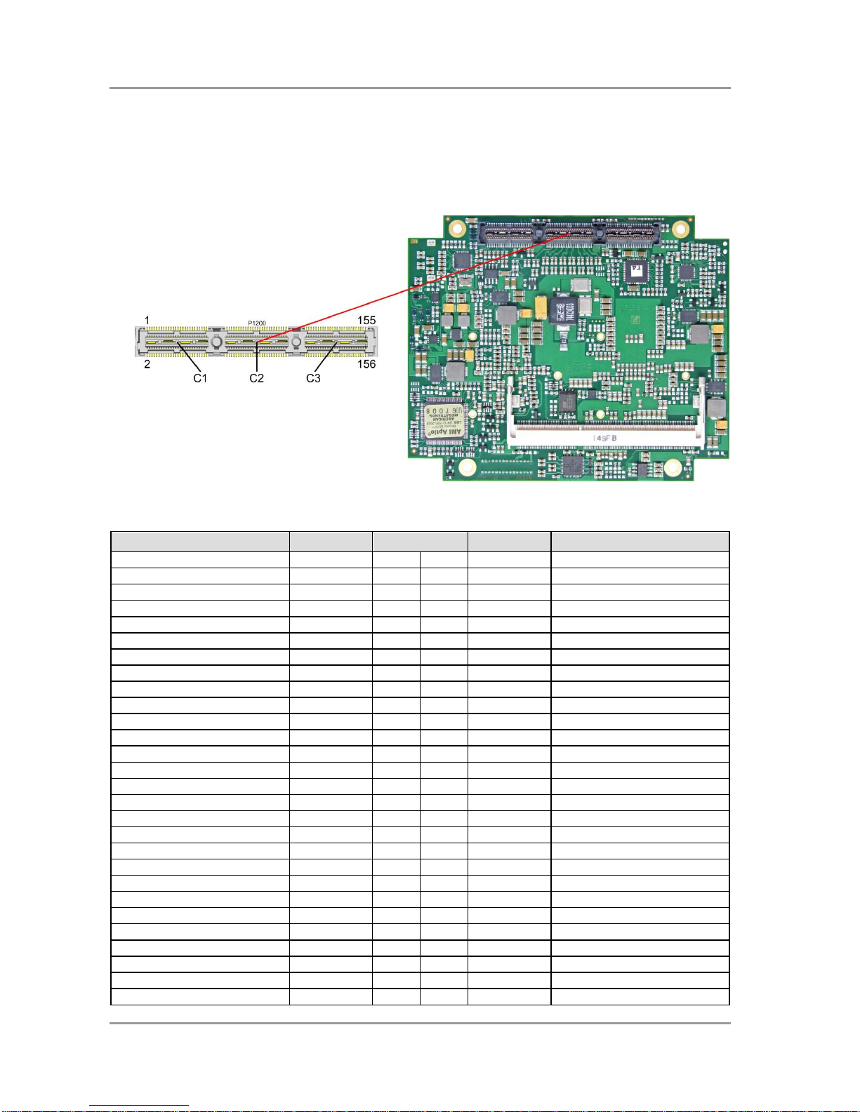
Chapter: Connectors Connector Map
page 14 ADL Embedded Solutions ADLQM67PC
3.1 Connector Map
Please use the connector map below for quick reference. Only connectors on the component side are
shown. For more information on each connector refer to the table below.
Ref-No.
Function
Page
P500
"SATA Interfaces"
p. 30
U600*
"Memory"
p. 17
P801/3
"LAN"
p. 28
P802/5
"COM1 and COM2"
p. 31
P804
"Audio"
p. 29
P807/10
"USB"
p. 27
P808/9
"LCD"
p. 25
P1200*
"PCIe/104 Connector"
p. 20
P1300
"DVI/HDMI"
p. 22
P1301
"DisplayPort"
p. 23
P1400
"System/SM-Bus"
p. 16
P1401
"VGA"
p. 24
P1402
"Power Supply"
p. 15
P1403
"Monitoring Functions"
p. 33
P1404
"GPIO"
p. 32
* not in the picture above (cf. bottom side of board)
Power Supply Chapter: Connectors
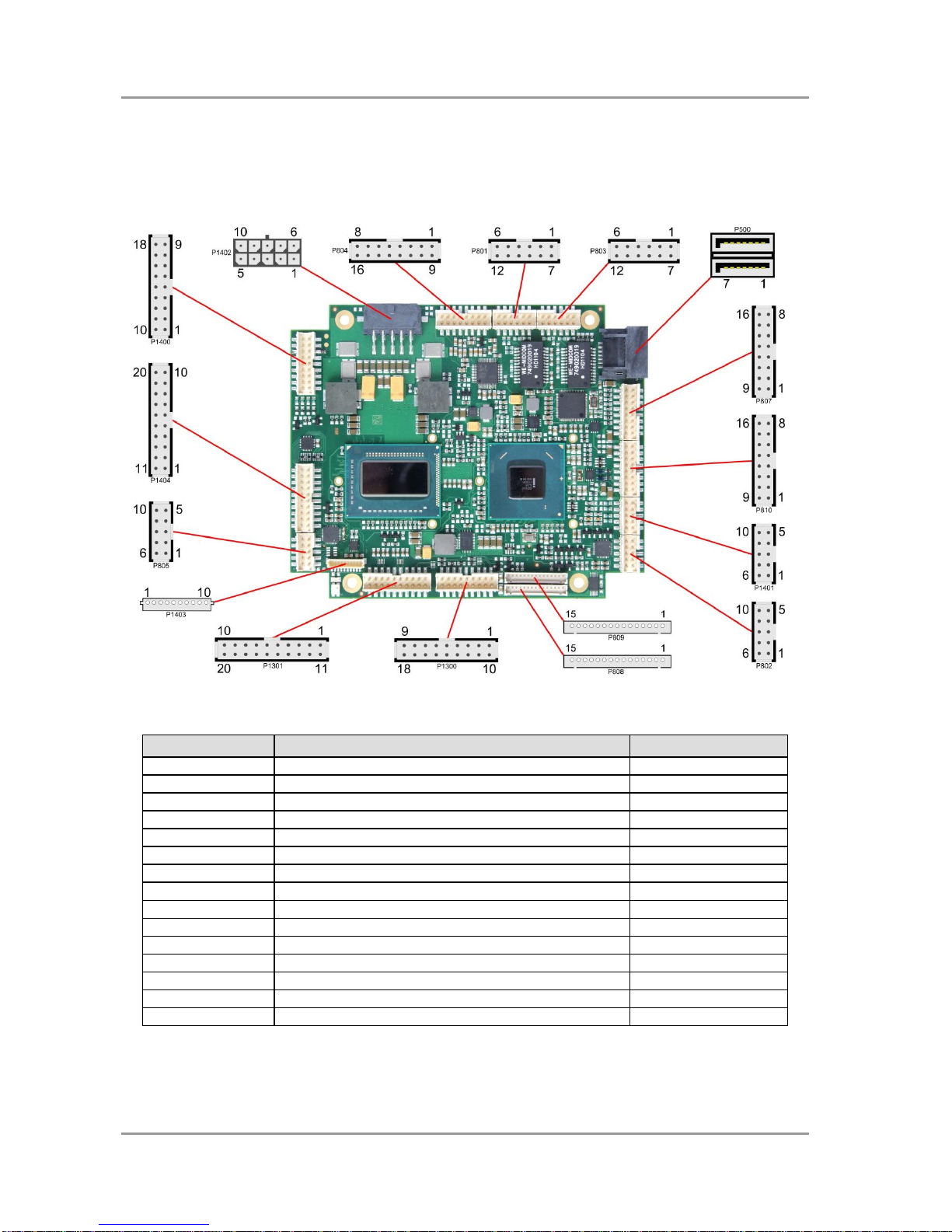
ADL Embedded Solutions ADLQM67PC page 15
3.2 Power Supply
The power supply of the hardware module is realized via a 2x5-pin connector (Molex PS 43045-10xx,
mating connector: Molex PS 43025-10xx). Both 5V VCC/SVCC and 12V need to be provided. The 12V
input can optionally be tied to 5V if 12V is not required by attached peripherals. It cannot, however, be left
unconnected.
CAUTION
The ADLQM67PC includes circuitry that will notify an intelligent power supply to shut down if the processor
reaches a critical temperature. This is achieved by deasserting the (low-active) PS_ON# signal found on
the SM-Bus connector. When PS_ON# is no longer pulled low, an intelligent power supply would take this
as a signal to shut down power. For this to work, PS_ON# must be connected to the power supply's PS_ON
input. If PS_ON# is not otherwise connected, the ADLQM67PC can be damaged beyond repair if a thermal
shutdown event occurs. In rare instances, if power is not shut down, the board will continue to heat up until
failure occurs.
NOTE
Since this is a 90 degree connector, the symbol in the drawing below represents the connector face as seen
from the side (PCB on bottom) rather than from above.
Description
Name
Pin
Name
Description
12 volt supply
12V
1
6
12V
12 volt supply
ground
GND
2
7
GND
ground
ground
GND
3
8
SVCC
standby-supply 5V
ground
GND
4
9
GND
ground
5 volt supply
VCC
5
10
VCC
5 volt supply
Chapter: Connectors System/SM-Bus
page 16 ADL Embedded Solutions ADLQM67PC
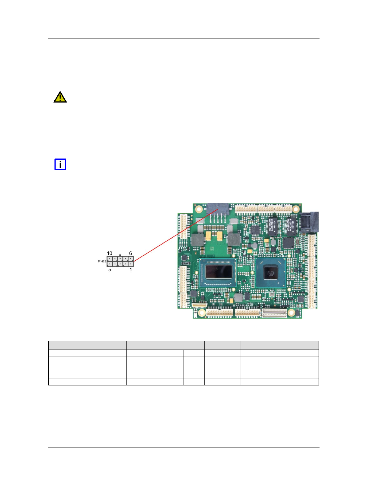
3.3 System/SM-Bus
Both SM-Bus signals, and signals for PS/2 keyboard, PS/2 mouse and speaker are provided through a
2x9pin connector (FCI 98424-G52-18LF, mating connector e.g. FCI 90311-018LF). For the #PSON signal,
please refer to the cautionary note in the chapter "Power Supply" (page 15).
Pinout 2x9pin connector:
Description
Name
Pin
Name
Description
speaker to 5V
SPEAKER
1
10
GND
ground
reset to ground
RSTBTN#
2
11
N/C
reserved
keyboard data
KDAT
3
12
KCLK
keyboard clock
mouse data
MDAT
4
13
MCLK
mouse clock
battery
BATT
5
14
VCC
5 volt supply
power supply on
PS-ON#
6
15
SMBCLK
SMB clock
standby supply 3.3V
S3.3V
7
16
SMBDAT
SMB data
power button
PWRBTN#
8
17
SMBALERT#
SMB alert
ground
GND
9
18
3.3V
3.3 volt supply

Memory Chapter: Connectors
ADL Embedded Solutions ADLQM67PC page 17
3.4 Memory
There is one conventional SO-DIMM204 socket available to equip the board with memory
(DDR3-1066/1333/1600). It is located on the bottom side of the board. For technical and mechanical
reasons it is possible that particular memory modules cannot be employed. Please ask your sales
representative for recommended memory modules.
With currently available SO-DIMM modules a memory extension up to 4 GByte is possible. The timing
parameters for different memory modules are automatically set by BIOS.
Pinout SO-DIMM204:
Description
Name
Pin
Name
Description
memory reference current
REF-DQ
1
2
GND
ground
ground
GND
3
4
DQ4
data 4
data 0
DQ0
5
6
DQ5
data 5
data 1
DQ1
7
8
GND
ground
ground
GND
9
10
DQS0#
data strobe 0 -
data mask 0
DM0
11
12
DQS0
data strobe 0 +
ground
GND
13
14
GND
ground
data 2
DQ2
15
16
DQ6
data 6
data 3
DQ3
17
18
DQ7
data 7
ground
GND
19
20
GND
ground
data 8
DQ8
21
22
DQ12
data 12
data 9
DQ9
23
24
DQ13
data 13
ground
GND
25
26
GND
ground
data strobe 1 -
DQS1#
27
28
DM1
data mask 1
data strobe 1 +
DQS1
29
30
RESET#
Reset
ground
GND
31
32
GND
ground
data 10
DQ10
33
34
DQ14
data 14
data 11
DQ11
35
36
DQ15
data 15
ground
GND
37
38
GND
ground
data 16
DQ16
39
40
DQ20
data 20
data 17
DQ17
41
42
DQ21
data 21
ground
GND
43
44
GND
ground
data strobe 2 -
DQS2#
45
46
DM2
data mask 2
data strobe 2 +
DQS2
47
48
GND
ground
ground
GND
49
50
DQ22
data 22

Chapter: Connectors Memory
page 18 ADL Embedded Solutions ADLQM67PC
Description
Name
Pin
Name
Description
data 18
DQ18
51
52
DQ23
data 23
data 19
DQ19
53
54
GND
ground
ground
GND
55
56
DQ28
data 28
data 24
DQ24
57
58
DQ29
data 29
data 25
DQ25
59
60
GND
ground
ground
GND
61
62
DQS3#
data strobe 3 -
data mask 3
DQM3
63
64
DQS3
data strobe 3 +
ground
GND
65
66
GND
ground
data 26
DQ26
67
68
DQ30
data 30
data 27
DQ27
69
70
DQ31
data 31
ground
GND
71
72
GND
ground
clock enables 0
CKE0
73
74
CKE1
clock enables 1
1.5 volt supply
1.5V
75
76
1.5V
1.5 volt supply
reserved
N/C
77
78
(A15)
reserved
SDRAM bank 2
BA2
79
80
A14
address 14
1.5 volt supply
1.5V
81
82
1.5V
1.5 volt supply
address 12 (burst chop)
A12/BC#
83
84
A11
address 11
address 9
A9
85
86
A7
address 7
1.5 volt supply
1.5V
87
88
1.5V
1.5 volt supply
address 8
A8
89
90
A6
address 6
address 5
A5
91
92
A4
address 4
1.5 volt supply
1.5V
93
94
1.5V
1.5 volt supply
address 3
A3
95
96
A2
address 2
address 1
A1
97
98
A0
address 0
1.5 volt supply
1.5V
99
100
1.5V
1.5 volt supply
Clock 0 +
CK0
101
102
CK1
clock 1 +
Clock 0 -
CK0#
103
104
CK1#
clock 1 -
1.5 volt supply
1.5V
105
106
1.5V
1.5 volt supply
address 10 (auto precharge)
A10/AP
107
108
BA1
SDRAM bank 1
SDRAM Bank 0
BA0
109
110
RAS#
row address strobe
1.5 volt supply
1.5V
111
112
1.5V
1.5 volt supply
write enable
WE#
113
114
S0#
chip select 0
column address strobe
CAS#
115
116
ODT0
on die termination 0
1.5 volt supply
1.5V
117
118
1.5V
1.5 volt supply
address 13
A13
119
120
ODT1
on die termination 1
Chip Select 1
S1#
121
122
N/C
reserved
1.5 volt supply
1.5V
123
124
1.5V
1.5 volt supply
reserved
(TEST)
125
126
REF-CA
reference current
ground
GND
127
128
GND
ground
data 32
DQ32
129
130
DQ36
data 36
data 33
DQ33
131
132
DQ37
data 37
ground
GND
133
134
GND
ground
data strobe 4 -
DQS4#
135
136
DQM4
data mask 4
data strobe 4 +
DQS4
137
138
GND
ground
ground
GND
139
140
DQ38
data 38
data 34
DQ34
141
142
DQ39
data 39
data 35
DQ35
143
144
GND
ground
ground
GND
145
146
DQ44
data 44
data 40
DQ40
147
148
DQ45
data 45
data 41
DQ41
149
150
GND
ground
ground
GND
151
152
DQS5#
data strobe 5 -
data mask 5
DQM5
153
154
DQS5
data strobe 5 +
ground
GND
155
156
GND
ground
data 42
DQ42
157
158
DQ46
data 46
data 43
DQ43
159
160
DQ47
data 47

Memory Chapter: Connectors
ADL Embedded Solutions ADLQM67PC page 19
Description
Name
Pin
Name
Description
ground
GND
161
162
GND
ground
data 48
DQ48
163
164
DQ52
data 52
data 49
DQ49
165
166
DQ53
data 53
ground
GND
167
168
GND
ground
data strobe 6 -
DQS6#
169
170
DQM6
data mask 6
data strobe 6
DQS6
171
172
GND
ground
ground
GND
173
174
DQ54
data 54
data 50
DQ50
175
176
DQ55
data 55
data 51
DQ51
177
178
GND
ground
ground
GND
179
180
DQ60
data 60
data 56
DQ56
181
182
DQ61
data 61
data 57
DQ57
183
184
GND
ground
ground
GND
185
186
DQS7#
data strobe 7 -
data mask 7
DQM7
187
188
DQS7
data strobe 7 +
ground
GND
189
190
GND
ground
data 58
DQ58
191
192
DQ62
data 62
data 59
DQ59
193
194
DQ63
data 63
ground
GND
195
196
GND
ground
SPD address 0
SA0
197
198
EVENT#
Event
3.3 volt supply
3.3V
199
200
SDA
SMBus data
SPD address 1
SA1
201
202
SCL
SMBus clock
termination current
VTT
203
204
VTT
termination current
Chapter: Connectors PCIe/104 Connector
page 20 ADL Embedded Solutions ADLQM67PC
3.5 PCIe/104 Connector
Expansion modules for the PCI-Express bus can be connected to the board using the PCIe/104™
connector. This is a "type 1" connector which offers full PCI-Express x16. "Stacking Error" functionality is
available. For specifics, please refer to the PCI/104-Express™ documentation (rev. 2.0).
Description
Name
Pin
Name
Description
reserved
N/C
1
2
PERST#
PCIe reset
3.3 volt supply
3.3V
3
4
3.3V
3.3 volt supply
display data channel clock
DDPC-CLK
5
6
N/C
reserved
display data channel data
DDPC-DAT
7
8
N/C
reserved
ground
GND
9
10
GND
ground
transmit lane 2 +
PET2
11
12
PET1
transmit lane 1 +
transmit lane 2 -
PET2#
13
14
PET1#
transmit lane 1 -
ground
GND
15
16
GND
ground
transmit lane 3 +
PET3
17
18
PET4
transmit lane 4 +
transmit lane 3 -
PET3#
19
20
PET4#
transmit lane 4 -
ground
GND
21
22
GND
ground
receive lane 2 +
PER2
23
24
PER1
receive lane 1 +
receive lane 2 -
PER2#
25
26
PER1#
receive lane 1 -
ground
GND
27
28
GND
ground
receive lane 3 +
PER3
29
30
PER4
receive lane 4 +
receive lane 3 -
PER3#
31
32
PER4#
receive lane 4 -
ground
GND
33
34
GND
ground
clock slot 1 +
PECLK1
35
36
PECLK0
clock slot 0 +
clock slot 1 -
PECLK1#
37
38
PECLK0#
clock slot 0 -
5 volt standby supply
SVCC
39
40
SVCC
5 volt standby supply
clock slot 2 +
PECLK2
41
42
PECLK3
clock slot 3 +
clock slot 2 -
PECLK2#
43
44
PECLK3#
clock slot 3 -
CPU direction
CPU_DIR
45
46
PWRGOOD
powergood
SMBus data
SMBDAT
47
48
PECLKx16
clock x16 slot +
SMBus clock
SMBCLK
49
50
PECLKx16#
clock x16 slot -
SMBus alert
SMBALERT
51
52
PSON#
PSU on
link reactivation
PEWAKE#
53
54
PEGENA#
PCIe graphics enable
ground
GND
55
56
GND
ground
Table of contents
Other ADL Motherboard manuals


