ADL S15PC User manual
Advanced DigitalLogicGmbH,EiserfelderStr. 316, Advanced DigitalLogic, Inc. 4411MorenaBlvd., Suite101
57080Siegen, Germany SanDiego, CA92117-4345
P. +49(0)271 2508100F. +49(0)271 250 81020 P. +1858490-0597F. +1858490-0599
e-mail: sales@adl-europe.com;web: http://www.adl-europe.com e-mail: sales@adl-usa.com;web: http://www.adl-usa.com
ADLS15PC
Manual
rev. 1.4


Contents
Advanced Digital Logic ADLS15PC page 3
Contents
0DocumentHistory...........................................................................................................................5
1Introduction.....................................................................................................................................6
1.1 Important Notes......................................................................................................................6
1.2 TechnicalSupport..................................................................................................................6
1.3 Warranty................................................................................................................................6
1.4 ReturnAuthorization...............................................................................................................6
1.5 Description of SafetySymbols................................................................................................7
2Overview........................................................................................................................................8
2.1 Features.................................................................................................................................8
2.2 Specificationsand Documents..............................................................................................10
3DetailedDescription......................................................................................................................11
3.1 PowerSupply.......................................................................................................................11
3.2 CPU.....................................................................................................................................11
3.3 Memory................................................................................................................................11
4Connectors...................................................................................................................................12
4.1 ConnectorMap.....................................................................................................................12
4.2 PowerSupply.......................................................................................................................13
4.3 System.................................................................................................................................14
4.4 Memory................................................................................................................................15
4.5 PC/104-Bus..........................................................................................................................18
4.6 PC/104-PlusBus..................................................................................................................20
4.7 VGA.....................................................................................................................................22
4.8 LCD......................................................................................................................................23
4.9 USB.....................................................................................................................................25
4.10 LAN......................................................................................................................................27
4.11 Audio....................................................................................................................................28
4.12 IDEInterface........................................................................................................................29
4.13 ParallelInterfaceLPT...........................................................................................................31
4.14 Serial InterfaceCOM1..........................................................................................................32
4.15 Serial InterfaceCOM2..........................................................................................................33
4.16 SMBus.................................................................................................................................34
4.17 Monitoring Functions............................................................................................................35
4.18 Fan......................................................................................................................................36
5BIOSSettings...............................................................................................................................37
5.1 RemarksforSetup Use........................................................................................................37
5.2 Top-Menü.............................................................................................................................37
5.3 StandardCMOSFeatures....................................................................................................38
5.3.1 IDEChannel0Master/Slave............................................................................................39
5.4 Advanced BIOSFeatures.....................................................................................................40
5.4.1 CPUFeature....................................................................................................................42
5.4.2 HardDiskBoot Priority.....................................................................................................43
5.5 Advanced Chipset Features..................................................................................................44
5.6 Integrated Peripherals..........................................................................................................45
5.6.1 OnChipIDEDevices........................................................................................................47
5.6.2 OnboardDevices.............................................................................................................48
5.6.3 PCI Express Root PortFunction.......................................................................................49

Contents
page 4 Advanced Digital Logic ADLS15PC
5.6.4 USB DeviceSetting..........................................................................................................50
5.7 PowerManagement Setup...................................................................................................51
5.7.1 HPETFeature..................................................................................................................52
5.7.2 Intel DTSFeature.............................................................................................................53
5.8 PnP/PCIConfiguration..........................................................................................................54
5.8.1 IRQ Resources.................................................................................................................55
5.9 PCHealthStatus..................................................................................................................56
5.10 Load Fail-SafeDefaults........................................................................................................58
5.11 Load Optimized Defaults......................................................................................................58
5.12 Set Password.......................................................................................................................58
5.13 Save&Exit Setup................................................................................................................58
5.14 ExitWithout Saving..............................................................................................................58
6BIOSupdate.................................................................................................................................59
7Mechanical Drawing......................................................................................................................60
7.1 PCB: Mounting Holes...........................................................................................................60
7.2 PCB: Pin1Dimensions........................................................................................................61
7.3 PCB: HeatSink....................................................................................................................62
7.4 Heat Spreader: ChassisMount.............................................................................................63
8TechnicalData..............................................................................................................................64
8.1 ElectricalData......................................................................................................................64
8.2 EnvironmentalConditions.....................................................................................................64
8.3 Thermal Specifications.........................................................................................................65
IAnnex:Post-Codes.......................................................................................................................66
II Annex:Resources........................................................................................................................69
AIO Range..................................................................................................................................69
BMemoryRange.........................................................................................................................69
CInterrupt....................................................................................................................................69
DPCI Devices..............................................................................................................................70
ESMB Devices............................................................................................................................70
Important Notes Chapter: DocumentHistory
Advanced Digital Logic ADLS15PC page 5
0DocumentHistory
Version Changes
0.1 first pre-release
0.9 first completeversion,todo: updatephotographstoG2
1.0 added SSDdescription,updated thermalspecs, minorcorrections
1.1 newphotographs, updated contact details,minorchanges
1.2 added pinoutforRS-422/RS-485 COMsoldering option,minorchanges
1.3 minorchanges
1.4 updated block diagram(ALC 885 EOL,8GBSSD),
added "3.3Vonly"warning forIDE, added noteconcerning PS_ON,
minorchanges
NOTE
Allcompanynames, brand names, and product namesreferredtointhismanual areregistered or
unregistered trademarksof theirrespectiveholdersand are, assuch, protected bynationaland
internationallaw.

Chapter: Introduction Important Notes
page 6 Advanced Digital Logic ADLS15PC
1Introduction
1.1ImportantNotes
Pleaseread thismanualcarefullybeforeyou startwiththe installation of thishardwaredevice.Toavoid
ElectrostaticDischarge (ESD)ortransientvoltage damage tothe board, adheretothe following rulesat
alltimes:
oYou must discharge yourbodyfromelectricitybeforetouching thisboard.
oToolsyou usemust be discharged fromelectricityaswell.
oPleasemakesurethat neitherthe boardyou want toinstall,northe unityou want toinstallthisboard
on, isenergized beforeinstallation iscompleted.
oPleasedo not touchanydevicesorcomponentson theboard.
CAUTION
Assoonasthe boardisconnected toaworking powersupply, touching the boardmayresultinelectrical
shock, even if the boardhasnot been switched on yet. Pleasealsonotethatthe mounting holesforheat
sinksareconnected toground, sowhen using an externallyACpowered device, asubstantialground
plane differential can occurifthe external device'sACpowersupplyorcabledoesnotinclude an earth
ground. Thiscouldalsoresultinelectricalshock when touching the deviceand the heatsink
simultaneously.
1.2Technical Support
Technicalsupportforthisproductcan be obtained inthefollowing ways:
oBy contacting oursupport staff at+1858-490-0597 or+49 (0)271 250 810 0
oBy contacting ourstaff via e-mailat support@adl-usa.com or support@adl-europe.com
oViaourwebsiteat www.adl-usa.com/support or www.adl-europe.com/support
1.3Warranty
Thisproductiswarranted tobe free of defectsinworkmanshipand material.ADL’ssoleobligation under
thiswarrantyistoprovide replacement partsorrepairservicesat no charge,except shipping cost. Such
defectswhichappearwithin12 monthsoforiginalshipmentofADL willbecovered, provided awritten
claimforserviceunderwarrantyisreceived byADL no less then 30 dayspriortothe end of thewarranty
period ofwithin30 daysofdiscoveryof the defect –whichevercomesfirst.Warrantycoverage is
contingent upon properhandling and operation ofthe product. Improperusesuchasunauthorized
modificationsorrepair, operation outside ofspecifiedratings, orphysicaldamage mayvoidanyservice
claimsunderwarranty.
1.4ReturnAuthorization
Allequipment returned toADL forevaluation, repair,credit return,modification,oranyotherreason must
be accompanied byan RMAnumber.Inordertoobtainan RMA authorization numberwewillneed a
completed RMAformsubmitted to support@adl-usa.com orfaxedto+1858-490-0599 fortheUSA office.
Forareturntothe European officeinGermany, pleasesubmitthe formto rma@adl-europe.com orfaxto
+49 (0)271 250 810 20.The formcanbe obtained atourwebsite: www.adl-usa.com orwww.adl-
europe.comunderthe Support section.Following areviewofthe information provided wewillissue a
returnauthorization number.
Description of SafetySymbols Chapter: Introduction
Advanced Digital Logic ADLS15PC page 7
1.5DescriptionofSafetySymbols
The following safetysymbolsareused inthisdocumentation.Theyareintended toalertthe readertothe
associated safetyinstructions.
ACUTERISKOFINJURY!
Ifyoudo not adheretothe safetyadvisenext tothissymbol,thereisimmediatedangertolifeand health
of individuals!
RISKOFINJURY!
Ifyoudo not adheretothe safetyadvisenext tothissymbol,thereisdangertolifeand healthof
individuals!
HAZARD TOINDIVIDUALS,ENVIRONMENT,DEVICES,ORDATA!
Ifyoudo not adheretothe safetyadvisenext tothissymbol,thereisobvioushazardtoindividuals,to
environment,tomaterials, ortodata.
NOTEORPOINTER
Thissymbolindicatesinformationthatcontributestobetterunderstanding.
Chapter: Overview Features
page 8 Advanced Digital Logic ADLS15PC
2Overview
2.1Features
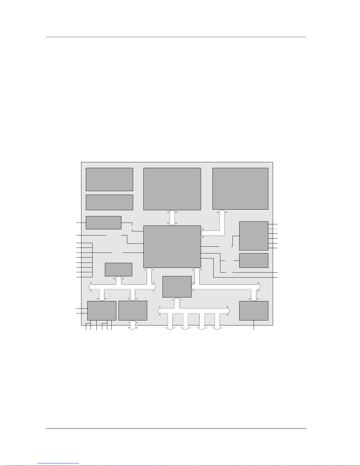
The ADLS15PCisahighlycomplexPC/104-Plusboardwhichincorporatescompletemotherboard
functionality.Equipped withan Intel®Atom™ processor(Z510 orZ530),it can accommodateup to2
GByteofRAM(DDR2-533)via SO-DIMM200.Italsoprovidesa16-bitISAbus(viaPC/104, no DMAand
memorytransferfunctionsavailable)aPCI bus(viaPC/104-Plus)and additional peripheral devicessuch
astwoserialinterfaces,GigabitEthernetinterface(LAN), an IDEinterface, an audiointerface(HDA7.1),
eight USBchannelsand CRT and LVDS/TFTsupport. Asan option,the ADLS15PCcan be equipped
withan onboardSSDof2, 4or8GBcapacity.The boardisbased on Intel®'sMenlow®platformwhichis
optimized forlowpowerconsumption. Relievingsystemdesignersofthe burden that theneed foractive
cooling normallypresents, Menlow®offersattractivenewpossibilitiesinthe embedded and mobile
markets.
Winbond®
W83627HG
LPC
PCI Intel®
82574L
1xSODIMM200
DDR2-RAM
(400/533MHz)
Power
VCCCore;VTT;
DDRVTT
1,5V;1,8V; 2,5V; 3,3V
Clock
ICS9UMS9633
BIOS
MS
IDE
RealTek®
ALC885/889 MIC
LINE IN
LINE OUT
HDA-Link
KB
USB1
USB2
USB3
PC/104plus
Slot 1
LAN
USB4
COM1
COM2
LPT
Watchdog
HOST
CRT
LCD LVDS18/24
Intel®SCH
US15WChipset
slave
SPDIFi
SPDIFo
PC/104plus
Slot 2
PC/104plus
Slot 3
USB5
USB6
USB7
USB8
PCIe
SMBus
Fintek®
F85226
LPC-to-ISA
FAN 1
FAN 2
AUX
Intel®Atom™CPU
Z510/ Z530
(1.1GHz/ 1.6GHz)
PC/104
PC/104plus
Slot 4
USB2.0
Pericom®
PI7C9X110
PCIe-to-PCI
MEMORY
SDVO-to-RGB-
DAC(CH7317A) SDVO
2/4/8GB
SSD
master
oProcessorIntel®Atom™(singlecore,512KB L2-cache, up to1.6GHzclockspeed)
oChipset Intel®SCHUS15Wwithintegrated graphicsadapter
oSO-DIMM200 socketforone DDR2-533 moduleof up to2GByte
oTwoserialinterfacesCOM1and COM2
oLANinterfaceEthernet 10/100/1000 (Base-T)
oIDEinterface
oOption: 2,4or8GBSSDonboard(IDEmaster.Soldering option: slave)
oPS2keyboard/ mouseinterface

Features Chapter: Overview
Advanced Digital Logic ADLS15PC page 9
oLPTinterface
oEight USB 2.0interfaces(7xhost, 1xhost/device)
oAWARD BIOS6.10
oCRT connection
oLCD connection via LVDS18/24Bit
oAC97/HDAcompatiblesound controllerwithSPDIFinand out
oRTCwithexternalCMOSbattery
o5Vsinglesupplyvoltage
oISA busviaPC/104 (full16bitsupport, no DMA and memorytransferfunctionality)
oPCI busviaPC/104-Plus(max.fourmasterdevices)
oSize:96 mm x90 mm

Chapter: Overview Specificationsand Documents
page 10 Advanced Digital Logic ADLS15PC
2.2SpecificationsandDocuments
Inmaking thismanualand forfurtherreading of technicaldocumentation the following documents,
specificationsand web-pageswereused and arerecommended.
§ISA Specification
IEEE996P
www.ieee.org
§PC/104™Specification
Version 2.5
www.pc104.org
§PC/104-Plus™Specification
Version 2.0
www.pc104.org
§PCI Specification
Version 2.3and 3.0
www.pcisig.com
§ACPI Specification
Version 3.0
www.acpi.info
§ATA/ATAPISpecification
Version 7Rev. 1
www.t13.org
§USB Specifications
www.usb.org
§SM-BusSpecification
Version 2.0
www.smbus.org
§Intel®Chipset Description
SCH Datasheet
www.intel.com
§Intel®ChipDescription
Atom®Datasheet
www.intel.com
§Winbond®ChipDescription
W83627HF
www.winbond-usa.com or www.winbond.com.tw
§Fintek® ChipDescription
F85226F Datasheet
www.fintek.com.tw
§Intel®ChipDescription
82574L Datasheet
www.intel.com

PowerSupply Chapter: Detailed Description
Advanced Digital Logic ADLS15PC page 11
3DetailedDescription
3.1PowerSupply
The powersupplyofthe hardwaremoduleiseffected viathe powerconnector. The boardonlyrequires
an operating voltage of 5volt±5%.
3.2CPU
The motherboardemploysan Intel®Atom™processoreitherwith1.1GHzorwith1.6GHzclock speed
(Z510/Z530).ThesearesinglecoreCPUswhichareoptimized forlowpowerconsumption whileatthe
sametimeproviding state-of-the-artcomputing performance.
The processorsinclude asecond level cache of 512 KByte.Theyalsooffermanyfeaturesknownfrom
the desktop range suchasMMX2, serialnumber,loadablemicrocode etc.
The Atom™ CPUiscombined withthe SCH US15Wchipset. The powerconsumption ofthesetwo
componentsneverexceeds5wattscombined.Therefore, passivecooling solutionswillbe sufficientfor
manysystemconfigurations.
3.3Memory
Thereisone conventionalSO-DIMM200 socket availabletoequipthe boardwithmemory.For
mechanical reasonsitispossiblethat particularmemorymodulescannot be employed. Pleaseaskyour
salesrepresentativeforrecommended memorymodules.
WithcurrentlyavailableSO-DIMM200 modulesamemory extension up to2GByteispossible(DDR2-
533). NOTE
The chipset doesnot support morethan 2GBofmemory.

Chapter: Connectors ConnectorMap
page 12 Advanced Digital Logic ADLS15PC
4Connectors
4.1ConnectorMap
Pleaseusethe connectormap belowforquick reference. Onlyconnectorson the component side are
shown. Formoreinformation on eachconnectorrefertothe tablebelow.
Ref-No. Function Page
P400 "IDEInterface" p. 29
U500* "Memory" p. 15
P800** "LAN" p. 27
P801 "Serial InterfaceCOM1" p. 32
P802** "Audio" p. 28
P803 "ParallelInterfaceLPT" p. 31
P804 "Serial InterfaceCOM2" p. 33
P805/6 "LCD" p. 23
P807/8** "USB" p. 25
P1200** "VGA" p. 22
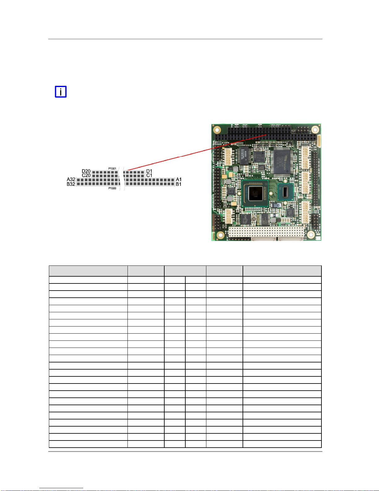
P1300/1 "PC/104-Bus" p. 18
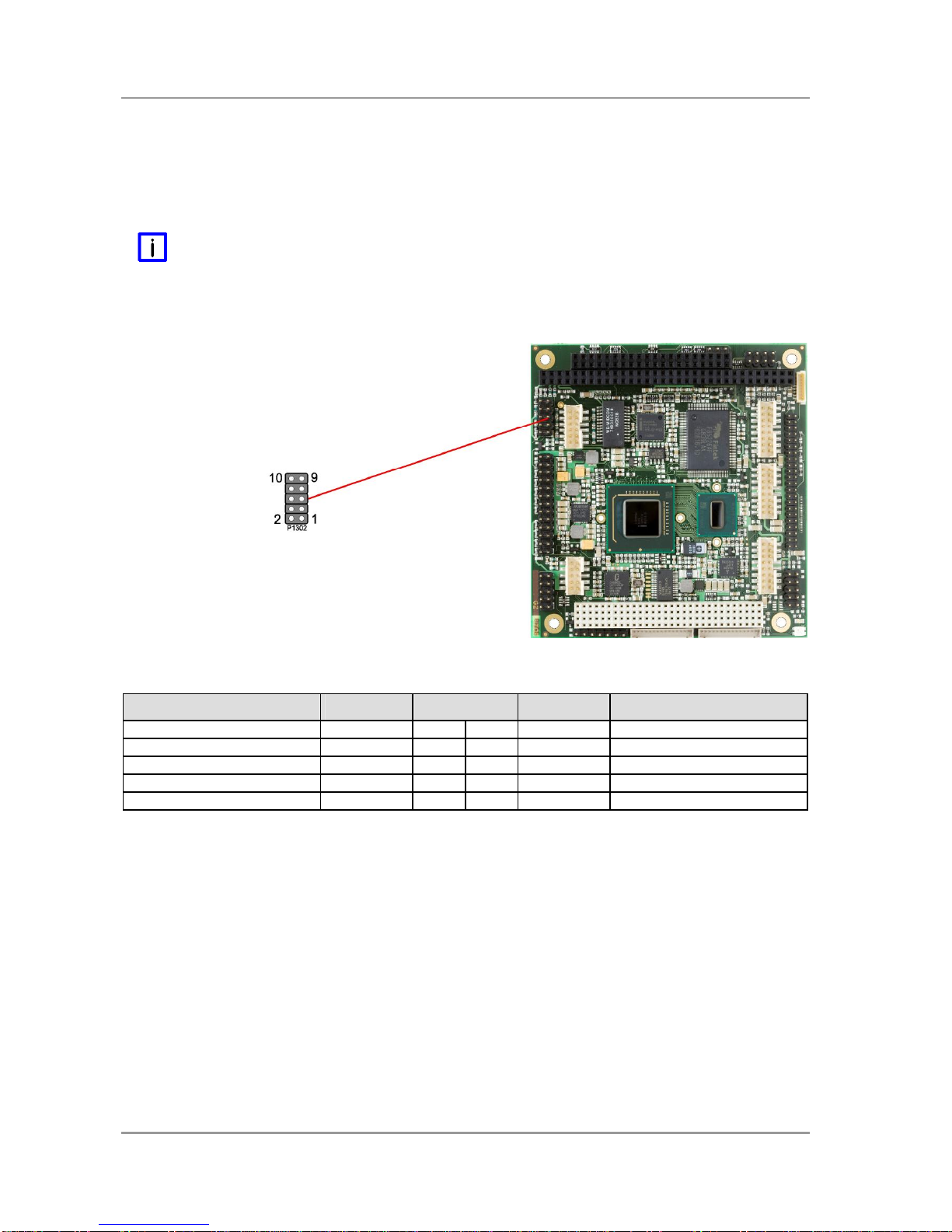
P1302 "System" p. 14
P1303 "PowerSupply" p. 13
P1304 "SMBus" p. 34
P1305 "MonitoringFunctions" p. 35
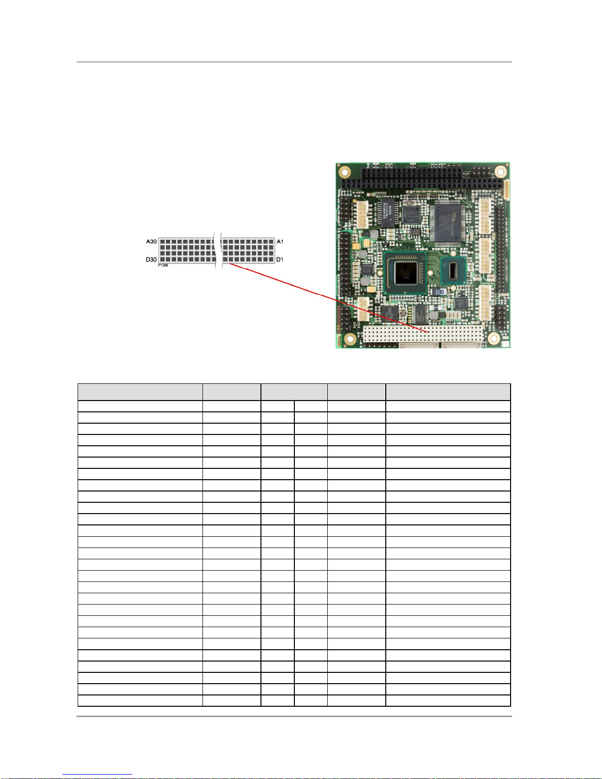
P1306 "PC/104-PlusBus" p. 20
P1307 "Fan" p. 36
*not inthe pictureabove(cf. bottomside of board)
** pinorientation holdsforboardrevision G2and later

PowerSupply Chapter: Connectors
Advanced Digital Logic ADLS15PC page 13
4.2PowerSupply
The connectorforthe powersupplyisastandardIDC socket connectorwithaspacing of2.54 mm.
The boardonlyrequiresan operating voltage of 5volt±5%. 3.3VoutputtothePC/104-Plusbusisthe
onlyoff-boardsupplyavailable.
Shouldadditional voltagesbe needed forPC/104 expansion cards, thesemust be provided externallyby
connecting the respectivepins(see below).
Formaximumcurrentavailability,it isrecommended touseboththispowerconnectorand the PC/104
connectorforpowersupply.
NOTE
For"Real TimeClock"an external battery(3.3V)mustbe connected. You can usepins1&3hereorthe
"System"connector(see next page).
CAUTION
The ADLS15PCincludescircuitrythat willnotifyan intelligentpowersupplytoshut downif the processor
reachesacritical temperature.Thisisachieved bydeasserting the (low-active)PS_ON#signalfound on
the SM-Busconnector. When PS_ON# ispulled high,itcan signalan intelligentpowersupplytoshut
down ifPS_ON# isconnected tothe powersupply'sPS_ONinput. If PS_ON#isnot otherwiseconnected,
the ADLS15PCcan be damaged beyond repairif athermalshutdowneventoccurs. Inrareinstances, if
powerisnot shut down, the boardwillcontinue toheat up untilfailureoccurs.
Description Name Pin Name Description
ground GND 1 2 VCC 5 voltsupply
CMOSbattery>=3volt VBAT 3 4 12V 12 voltsupply
-5volt supply -5V 5 6 -12V -12 voltsupply
ground GND 7 8 VCC 5 voltsupply
Chapter: Connectors System
page 14 Advanced Digital Logic ADLS15PC
4.3System
The systemconnector, whichhasthe mainfunctionsthat arenecessary tostart the board,isprovided via
astandardIDC socket connectorwithaspacing of 2.54mm.
Thisconnectorsupportsthe following interfaces: PS/2keyboard, PS/2mouse, speaker, externalRTC-
battery and reset ofthe board.
NOTE
For"Real TimeClock"an external battery(3.3V)mustbe connected. Connect "+"toVBATand "-"to
GND.
Description Name Pin Name Description
speakerto5volt SPEAKER 1 2 GND ground
reset toground RESET# 3 4 KLOCK# keyboardlock
keyboardData KDAT 5 6 KCLK keyboardclock
mousedata MDAT 7 8 MCLK mouseclock
CMOSbattery 3volt VBAT 9 10 VCC 5 voltsupply

Memory Chapter: Connectors
Advanced Digital Logic ADLS15PC page 15
4.4Memory
Thereisone conventionalSO-DIMM200 socket availabletoequipthe boardwithmemory(DDR2-533).It
islocated onthe bottomside of the board.Formechanicalreasonsitispossiblethatparticularmemory
modulescannot be employed.Pleaseaskyoursalesrepresentativeforrecommended memory modules.
WithcurrentlyavailableSO-DIMMmodulesamemory extension up to2GByteispossible.The timing
parametersfordifferentmemory modulesareautomaticallyset byBIOS.
NOTE
The chipset doesnot support morethan 2GBofmemory.
Description Name Pin Name Description
memoryreferencecurrent REF 1 2 REF memoryreferencecurrent
ground GND 3 4 GND ground
data0 DQ0 5 6 DQ4 data4
data1 DQ1 7 8 DQ5 data5
2.5volt supply 2.5V 9 10 2.5V 2.5volt supply
datastrobe 0 DQS0 11 12 DQM0 datamask0
data2 DQ2 13 14 DQ6 data6
ground GND 15 16 GND ground
data3 DQ3 17 18 DQ7 data7
data8 DQ8 19 20 DQ12 data12
2.5volt supply 2.5V 21 22 2.5V 2.5volt supply
data9 DQ9 23 24 DQ13 data13
datastrobe 1 DQS1 25 26 DQM1 datamask1
ground GND 27 28 GND ground
data10 DQ10 29 30 DQ14 data14
data11 DQ11 31 32 DQ15 data15
2.5volt supply 2.5V 33 34 2.5V 2.5volt supply
clock CK0 35 36 2.5V 2.5volt supply
clock CK0# 37 38 2.5V 2.5volt supply
ground GND 39 40 GND ground
data16 DQ16 41 42 DQ20 data20
data17 DQ17 43 44 DQ21 data21

Chapter: Connectors Memory
page 16 Advanced Digital Logic ADLS15PC
Description Name Pin Name Description
2.5volt supply 2.5V 45 46 2.5V 2.5volt supply
datastrobe 2 DQS2 47 48 DQM2 datamask2
data18 DQ18 49 50 DQ22 data22
ground GND 51 52 GND ground
data19 DQ19 53 54 DQ23 data23
data24 DQ24 55 56 DQ28 data28
2.5volt supply 2.5V 57 58 2.5V 2.5volt supply
data25 DQ25 59 60 DQ29 data29
datastrobe 3 DQS3 61 62 DQM3 datamask3
ground GND 63 64 GND ground
data26 DQ26 65 66 DQ30 data30
data27 DQ27 67 68 DQ31 data31
2.5volt supply 2.5V 69 70 2.5V 2.5volt supply
datacheck bit 0 CB0 71 72 CB4 datacheck bit 4
datacheck bit 1 CB1 73 74 CB5 datacheck bit 5
ground GND 75 76 GND ground
datastrobe 8 DQS8 77 78 DQM8 datamask8
datacheck bit 2 CB2 79 80 CB6 datacheck bit 6
2.5volt supply 2.5V 81 82 2.5V 2.5volt supply
datacheck bit 3 CB3 83 84 CB7 datacheck bit 7
reserved N/C 85 86 N/C reserved
ground GND 87 88 GND ground
clock CK2 89 90 GND ground
clock CK2# 91 92 2.5V 2.5volt supply
2.5volt supply 2.5V 93 94 2.5V 2.5volt supply
clockenables1 CKE1 95 96 CKE0 clockenables0
reserved N/C 97 98 N/C reserved
address12 A12 99 100 A11 address11
address9 A9 101 102 A8 address8
ground GND 103 104 GND ground
address7 A7 105 106 A6 address6
address5 A5 107 108 A4 address4
address3 A3 109 110 A2 address2
address1 A1 111 112 A0 address0
2.5volt supply 2.5V 113 114 2.5V 2.5volt supply
address10 A10 115 116 BA1 SDRAM bank1
SDRAM bank0 BA0 117 118 RAS# rowaddressstrobe
writeenable WE# 119 120 CAS# columnaddress strobe
chipselect S0# 121 122 S1# chipselect
reserved N/C 123 124 N/C reserved
ground GND 125 126 GND ground
data32 DQ32 127 128 DQ36 data36
data33 DQ33 129 130 DQ37 data37
2.5volt supply 2.5V 131 132 2.5V 2.5volt supply
datastrobe 4 DQS4 133 134 DQM4 datamask4
data34 DQ34 135 136 DQ38 data38
ground GND 137 138 GND ground
data35 DQ35 139 140 DQ39 data39
data40 DQ40 141 142 DQ44 data44
2.5volt supply 2.5V 143 144 2.5V 2.5volt supply
data41 DQ41 145 146 DQ45 data45
datastrobe 5 DQS5 147 148 DQM5 datamask5
ground GND 149 150 GND ground
data42 DQ42 151 152 DQ46 data46
data43 DQ43 153 154 DQ47 data47

Memory Chapter: Connectors
Advanced Digital Logic ADLS15PC page 17
Description Name Pin Name Description
2.5volt supply 2.5V 155 156 2.5V 2.5volt supply
2.5volt supply 2.5V 157 158 CK1# clock
ground GND 159 160 CK1 clock
ground GND 161 162 GND ground
data48 DQ48 163 164 DQ52 data52
data49 DQ49 165 166 DQ53 data53
2.5volt supply 2.5V 167 168 2.5V 2.5volt supply
datastrobe 6 DQS6 169 170 DQM6 datamask6
data50 DQ50 171 172 DQ54 data54
ground GND 173 174 GND ground
data51 DQ51 175 176 DQ55 data55
data56 DQ56 177 178 DQ60 data60
2.5volt supply 2.5V 179 180 2.5V 2.5volt supply
data57 DQ57 181 182 DQ61 data61
datastrobe 7 DQS7 183 184 DQM7 datamask7
ground GND 185 186 GND ground
data58 DQ58 187 188 DQ62 data62
data59 DQ59 189 190 DQ63 data63
2.5volt supply 2.5V 191 192 2.5V 2.5volt supply
SPDdata SDA 193 194 SA0 SPDaddress
SPDclock SCL 195 196 SA1 SPDaddress
3.3volt supply 3.3V 197 198 SA2 SPDaddress
reserved N/C 199 200 N/C reserved
Chapter: Connectors PC/104-Bus
page 18 Advanced Digital Logic ADLS15PC
4.5PC/104-Bus
AnonboardLPC-to-ISAbridge (Fintek®F85226F)makesit possibletoexpand thefunctionalityof the
boardwithadditionalPC/104 cards. Thisinterfaceoffers full16bitISAcompliance.Forfurtherinformation
on thisinterfacepleaserefertothe PC/104 specifications(see"Specificationsand Documents",p. 10).
NOTE
The chipset used on thisboarddoesnot support ISA-DMA functionality.
Pinning ofthe standard8bitPC/104 connector.
Description Name Pin Name Description
ISA -IO channel check IOCHK# A1 B1 GND ground
ISA –data7 SD7 A2 B2 RSTDRV reset drive
ISA –data6 SD6 A3 B3 VCC 5 voltsupply
ISA –data5 SD5 A4 B4 IRQ9 ISA –interrupt 9(2)
ISA –data4 SD4 A5 B5 -5V -5volt supply
ISA –data3 SD3 A6 B6 (DRQ2) reserved
ISA –data2 SD2 A7 B7 -12V -12 voltsupply
ISA –data1 SD1 A8 B8 IOCHRDY ISA –IO channelready
ISA –data0 SD0 A9 B9 12V 12 voltsupply
ISA –IO channelready IOCHRDY A10 B10 N/C reserved
ISA –addressenable AEN A11 B11 SMEMW# ISA –systemmemorywrite
ISA –address19 SA19 A12 B12 SMEMR# ISA –systemmemoryread
ISA –address18 SA18 A13 B13 IOW# ISA –IO write
ISA –address17 SA17 A14 B14 IOR# ISA –IO read
ISA –address16 SA16 A15 B15 (DACK3#) reserved (pulled high)
ISA –address15 SA15 A16 B16 (DRQ3) reserved
ISA –address14 SA14 A17 B17 (DACK1#) reserved (pulled high)
ISA –address13 SA13 A18 B18 (DRQ1) reserved
ISA –address12 SA12 A19 B19 REFRESH# ISA –refresh
ISA –address11 SA11 A20 B20 SYSCLK ISA –systemclock
ISA –address10 SA10 A21 B21 IRQ7 ISA –interrupt 7
ISA –address9 SA9 A22 B22 IRQ6 ISA –interrupt 6
ISA –address8 SA8 A23 B23 IRQ5 ISA –interrupt 5
ISA –address7 SA7 A24 B24 IRQ4 ISA –interrupt 4
PC/104-Bus Chapter: Connectors
Advanced Digital Logic ADLS15PC page 19
Description Name Pin Name Description
ISA –address6 SA6 A25 B25 IRQ3 ISA –interrupt 3
ISA –address5 SA5 A26 B26 (DACK2#) reserved (pulled high)
ISA –address4 SA4 A27 B27 T/C ISA –terminal count
ISA –address3 SA3 A28 B28 BALE ISA –addresslatchen.
ISA –address2 SA2 A29 B29 VCC 5 voltsupply
ISA –address1 SA1 A30 B30 OSC ISA –14,318MHz
ISA –address0 SA0 A31 B31 GND ground
ground GND A32 B32 GND ground
Pinning ofthe 16 bit expansion PC/104 connector.
Description Name Pin Name Description
ground GND C0 D0 GND ground
ISA –bytehigh enable SBHE# C1 D1 MEMCS16# ISA –memorychipselect
ISA –latched address23 LA23 C2 D2 IOCS16# ISA –IO chipselect
ISA –latched address22 LA22 C3 D3 IRQ10 ISA –interrupt 10
ISA –latched address21 LA21 C4 D4 IRQ11 ISA –interrupt 11
ISA –latched address20 LA20 C5 D5 IRQ12 ISA –interrupt 12
ISA –latched address19 LA19 C6 D6 IRQ15 ISA –interrupt 15
ISA –latched address18 LA18 C7 D7 IRQ14 ISA –interrupt 14
ISA –latched address17 LA17 C8 D8 (DACK0#) reserved (pulled high)
ISA –memoryread MEMR# C9 D9 (DRQ0) reserved
ISA –memorywrite MEMW# C10 D10 (DACK5#) reserved (pulled high)
ISA –data8 SD8 C11 D11 (DRQ5) reserved
ISA –data9 SD9 C12 D12 (DACK6#) reserved (pulled high)
ISA –data10 SD10 C13 D13 (DRQ6) reserved
ISA –data11 SD11 C14 D14 (DACK7#) reserved (pulled high)
ISA –data12 SD12 C15 D15 (DRQ7) reserved
ISA –data13 SD13 C16 D16 VCC 5 voltsupply
ISA –data14 SD14 C17 D17 MASTER# ISA –busmaster
ISA –data15 SD15 C18 D18 GND ground
reserved N/C C19 D19 GND ground
Chapter: Connectors PC/104-PlusBus
page 20 Advanced Digital Logic ADLS15PC
4.6PC/104-PlusBus
Expansion cardscan be connected tothe boardusing the PCI connectorfirstintroduced withthePC/104-
Plusstandard. AmaximumoffourPC/104-Pluscardsaresupported.
The interrupt routing and the IDSELsignalsforthe expansion cardsarespecified inthe PC/104-Plus
specification (see "Specificationsand Documents", p.10).
Description Name Pin Name Description
ground GND A1 B1 N/C reserved
5volt-IObufferpower VCCIO A2 B2 AD2 PCI –address/data2
PCI –address/data5 AD5 A3 B3 GND ground
PCI –com/byteenable0 CBE0# A4 B4 AD7 PCI –address/data7
ground GND A5 B5 AD9 PCI –address/data9
PCI –address/data11 AD11 A6 B6 VCCIO 5volt-IObufferpower
PCI –address/data14 AD14 A7 B7 AD13 PCI –address/data13
3.3volt supply 3.3V A8 B8 CBE1# PCI –com/byteenable1
PCI –systemerror SERR# A9 B9 GND ground
ground GND A10 B10 PERR# PCI –parityerror
PCI –stop stop# A11 B11 3.3V 3.3volt supply
3.3volt supply 3.3V A12 B12 TRDY# PCI –target ready
PCI –frame FRAME# A13 B13 GND ground
ground GND A14 B14 AD16 PCI –address/data16
PCI –address/data18 AD18 A15 B15 3.3V 3.3volt supply
PCI –address/data21 AD21 A16 B16 AD20 PCI –address/data20
3.3volt supply 3.3V A17 B17 AD23 PCI –address/data23
PCI –IDselectslot 1 IDSEL0 A18 B18 GND ground
PCI –address/data24 AD24 A19 B19 CBE3# PCI –com/byteenable3
ground GND A20 B20 AD26 PCI –address/data26
PCI –address/data29 AD29 A21 B21 VCC 5 voltsupply
5voltsupply VCC A22 B22 AD30 PCI –address/data30
PCI –busrequest slot 1 REQ0# A23 B23 GND ground
ground GND A24 B24 REQ2# PCI –busrequest slot 3
PCI –busgrant slot4 GNT1# A25 B25 VCCIO 5volt-IObufferpower
5voltsupply VCC A26 B26 CLK0 PCI –clockslot 1
PCI –clockslot 3 CLK2 A27 B27 VCC 5 voltsupply
Table of contents
Other ADL Motherboard manuals


