Aiwa XP-770 User manual

SPECIFICATIONS
Tracking system: 1-beam iaser
Laser pickup: Semiconductor iaser
D/A conversion: 8-times oversampiing digitai fiiter +1-bit
DAC
Frequency response:20 -20,000 Hz
output: PHONES/LiNE OUT: stereo mini-jack
Msximum output: 12mW+12mW (EiAJ160hmsatlkHz)
500mV (47 kohms at 1kHz)
Powsr suppiy: DC 3Vusing lwo size AA (LR6) aikaiine
batteries
<770AU,779U,AHR>
DC 2.4V using commercially avaiiabie
rechargeable batteries
<AEZ,AK>
DC 2.4V using suppiied rechargeable
batteries
AC house current using the suppiied AC
adaptor
146.9 (W) x 28 (H) x158.5 (D) mm
(5 718X1318X6‘1. in.)
240 grams (8.4 oz.) without batteries
Dimensions:
Weight:
<AC Adaptor>
Rated voitage: <770AU,779AU>
AC-A62U :AC 120V,60HZ
dHR>
AC-A62 :AC 11 O-120V /220-240V,
selectable 50/60Hz
<AEZ,AK>
AC-A62: AC 230 V, 50 iiz
<Suppiied headphones HP-MO13> (AEZ ONLY)
Type: in-ear type
impedance: 16 ohms
Sensitivity: f07 dBlmW
cRecomendsd commercially avaiiabie headphones>
Type: in ear typelVerticai type/headband type
impsdance: 16-32 ohms
Sensitivity: 100-109 dB/mW
<Car audio cassetts adsptor> (779AU ONLY)
Frequency range: 50-20,000 Hz (it may differ depending
on type of your cassette car stereo)
Cord iength: 1,5 m(4 feet 11 inches)
Dimensions: 102.4 (W) x12.1 (H) x63.8 (D) mm
(4’/8x ‘/, x25/, inches)
Weight Approx. 41 g(1.4 OZ)
<Car battery adaptor> (779AU ONLY)
input voitage: DC 12 V124 V
Output voitage: DC 6V300 mA
Cord iength 1.5 m(4 feet 11 inches)
Weight Approx. 53g (1.9 OZ)
●Design and specifications are subject to change without
notice.
–2–
w
w
w
.
x
i
a
o
y
u
1
6
3
.
c
o
m
Q
Q
3
7
6
3
1
5
1
5
0
9
9
2
8
9
4
2
9
8
T
E
L
1
3
9
4
2
2
9
6
5
1
3
9
9
2
8
9
4
2
9
8
0
5
1
5
1
3
6
7
3
Q
Q
TEL 13942296513 QQ 376315150 892498299
http://www.xiaoyu163.com

PROTECTION OF EYES FROM LASER BEAM
This set employs laser. Therefore, be sure to follow carefully
the instructions below when servicing.
WARNING!!
WHEN SERVICING, DO NOT APPROACH THE LASER EXIT
WITH THE EYE TOO CLOSELY. IN CASE IT IS NECESSARY
TO CONFIRM LASER BEAM EMISSION. BE SURE TO
OBSERVE FROM ADISTANCE OF MORE THAN 30crn
FROM THE SURFACE OF THE OBJECTIVE LENS ON THE
OPTICAL PICK-UP BLOCK.
Caution: Invisible laser radiation when
open and intertocke defeated avoid expo-
sure to beam.
Advarsel: Usynlig Iaaeretiling ved &bning,
n& sikkerhedsafbrydere er ude af funktion.
Undg& udsattelse for str~ling.
DURING SERVICING
CAUTION
Use of controls or adjustments or performance of pr&adures
other than those specified herein may result in hazardous red{-
ation exposure.
AllENTION
L’utilisation de commandes, r6glages ou prw%cfures autres que
ceux sp6cifi6epeutentraher unedangereuseexpositionaux
radiations.
ADVARSEL!
Usynlig IaseratMlng ved Mining, n& sikkerhedsafbrydereer ude
af funktion. Undg& udssettelse for strAling.
This Compact Disc player is classified as a CLASS 1USER
product.
The CLASS 1LASER PRODUCT label is located on the rear
exterior.
VAROITUS!
Laiteen K/iytMminen muulla kuin tiias~ k~yttbohjeessa mainit-
ulla tavalla saattaa altiataa k@t-taj&i turvallisuusluokan 1yiit-
WvAlle nAkymMt&ni411e laaeraMeilylle.
VARNING!
Om apparaten anvi+nds pa annat sMt &I vad som specificeraa
idenna brukaanvising, ken anv~daren utsWtas fbr osynling
laserstr&ning, som Werskrider grtinsen f& Iaserklaaa 1.
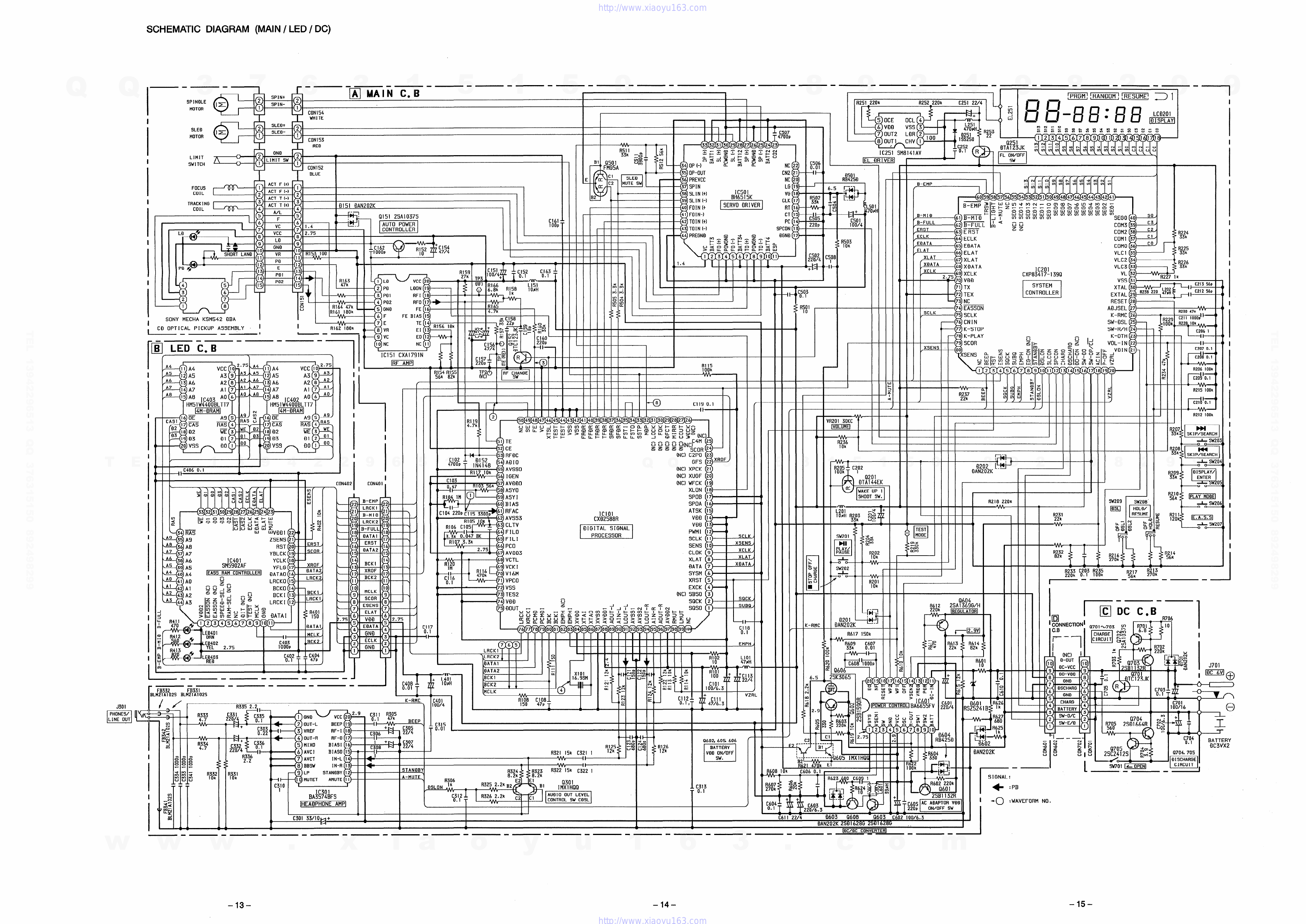
Precaution to replace Optical block
(KSS -5420)
Body or clotheselectrostaticpotentialcould
ruinlaserdiodein the opticalblock,Be sure
ground body and workbench, and use care the
clothes do not touch the diode.
1) After the connection, remove solder shown in
right figure.
1910
—
-3-
w
w
w
.
x
i
a
o
y
u
1
6
3
.
c
o
m
Q
Q
3
7
6
3
1
5
1
5
0
9
9
2
8
9
4
2
9
8
T
E
L
1
3
9
4
2
2
9
6
5
1
3
9
9
2
8
9
4
2
9
8
0
5
1
5
1
3
6
7
3
Q
Q
TEL 13942296513 QQ 376315150 892498299
http://www.xiaoyu163.com

ELECTRICAL MAIN PARTS LIST
IIfczm’t understandfor Description please kindly refer to” REFERENCE NAME LIST”. I
REF.NO. PARTNO. KANRI DESCRIPTION
NO.
IC
87-A20-144-040
87-A2O-894-O1O
87-A2O-897-O1O
87-A20-574-010
87-A2O-614-O1O
87-A2O-892-O1O
87-A20-928-040
87-A2O-963-O1O
88-HC4-608-O1O
TRANSISTOR
DIODE
MAIN C.B
Clol
C102
C103
C104
C105
C108
Clll
C112
C113
C115
C116
C117
C118
C119
C121
C122
C123
C124
C151
C152
C154
C155
C156
C157
C158
C159
C160
C161
C162
C163
C201
C202
C203
89-110-373-080
87-026-608-080
87-026-211-080
87-026-580-080
87-026-585-080
87-026-678-080
89-211-323-080
87-A3O-21O-O4O
87-A30-183-040
89-113-695-680
87-A30-203-080
89-416-643-080
89-324-123-080
87-020-331-080
87-A40-246-080
84-XMC-624-080
87-002-882-080
87-A40-220-080
87-016-557-080
87-010-186-080
87-016-526-080
87-012-156-080
87-010-992-080
87-012-188-080
87-016-558-080
87-010-196-080
87-016-296-080
87-010-184-080
87-010-196-080
87-010-196-080
87-010-196-080
87-010-831-080
87-012-197-080
87-012-197-080
87-012-272-080
87-012-272-080
87-010-502-040
87-010-196-080
87-010-501-040
87-010-501-040
87-010-501-040
87-012-156-080
87-010-314-080
87-010-313-080
87-012-156-080
87-010-322-080
87-010-178-080
87-010-196-080
87-010-502-040
87-010-805-080
87-010-196-080
C-IC,BA3574BFS
C-IC,BH6515K
C-IC,BA6655FV
IC,SM5902AF
c-Ic,HM51W4400BLTT/BTT-7/8
C-IC,CXD2588R
C-IC,sM814lAV
C-IC,CXA1791N
C-IC,CXP83417-139Q
CHIP-TR,2SA1037
C-TR,DTC 123JR
C-TR,DTA144EK
C-TR,DTA123JK
C-TR,INK1HQQ
C-TR,FMG5A
C-TR,2SB1132R
CATR,2SB1590KQR
C-TR,2SD1628G
C-TR,2SA1369G/H
C-FET,2SK3065
C-TR,2SD1664R
C-TR,2SC2412KS
s
CHIP-DIODE,DAN202K
DIODE,IN4148T-72
C-DIODE,1SS250
C-DIODE,RB425D
COZENER,RSZ5241B
CAP,E 100-6.3SF
CAP,CHIP4700P
C-CAP,S 0.47-16BK
C-CAP,S 220P-50CH
C-CAP,S 0.047-25B
C-CAP,U 47P-50CH
C-CAP,TN47-6.3F93B
CHIPCAPACITOR,0.1-25
C-CAP,TN 22-4SV(A]
CHIPCAPACITOR3300P(K)
CHIPCAPACITOR,0.1-25
C-CAF,U,O.1-16F
C-CAP,U 150P-50CH
C-CAP,U 150P-50CH
C-CAP,U 680P-50B
C-CAP,U 680P-50B
CAP ELECTGAS 100/4
CHIPCAPACITOR,0.1-25
E/CAPGAS 47-4
E/CAFGAS 47-4
E/C?@GAS 47-4
C-CAP,S 220P-50CH
C-CAP,S 22P-50V
CAP,CHIP 18P
C-CAP,S 220P-50CH
C-CAP,S 1OOP-5OCH
CHIPCAP 1000P
CHIPCAPACITOR,0.1-25
CAP ELECTGAS 100/4
CAP,S 1-16
CHIPCAPACITOR,0.1-25
REF.NO. PARTNO. KANRI DESCRIPTION
NO.
C206
C207
C208
C209
C21O
C211
C212
C213
C251
C252
C301
C303
C305
C306
C307
C308
C31O
C311
C312
C313
C315
C321
C322
C331
C332
C333
C334
C335
C336
C341
C401
C408
C501
C502
C503
C504
C505
C506
C507
C508
C511
C601
C602
C603
C604
C605
C606
C607
C608
C609
C61O
C611
EL251
FB331
FB332
FB341
FB342
J301
L101
L151
L201
L202
L251
L501
L601
LCD201
R606
SW201
SW202
SW203
4-
87-010-805-080
87-010-196-080
87-010-196-080
87-010-196-080
87-010-196-080
87-010-178-080
87-012-337-080
87-012-337-080
87-016-296-080
87-AIO-811-080
87-010-077-080
87-012-141-080
87-016-296-080
87-010-805-080
87-016-296-080
S7-O1O-8O5-O8O
87-010-805-080
87-010-196-080
87-010-196-080
87-010-196-080
87-018-134-080
87-010-805-080
87-010-805-080
87-010-503-040
87-010-503-040
87-010-178-080
87-010-178-080
87-010-196-080
87-010-196-080
87-010-178-080
87-010-502-040
87-010-197-080
87-010-502-040
87-010-503-040
87-010-196-080
87-010-805-080
87-012-156-080
87-010-197-080
87-010-186-080
87-010-805-080
87-010-185-080
87-010-503-040
87-010-079-040
87-A1O-5O5-O8O
87-010-196-080
87-012-156-080
87-010-831-080
87-010-197-080
87-010-178-080
87-010-805-080
87-010-196-080
87-016-296-080
88-HC4-61O-O1O
87-A50-190-080
87-A50-190-080
87-A50-190-080
87-A50-190-080
85-HC5-616-O1O
87-005-781-080
87-005-780-080
87-005-780-080
87-005-781-080
87-A50-281-080
87-005-843-080
88-HC4-615-040
88-HC4-607-O1O
87-022-525-080
87-A90-095-080
87-A90-095-080
87-A90-095-080
CAP, S 1-16
CHIPCAPACITOR,0.1-25
CHIPCAP 1000P
C-CAP,U56P-50CH
C-CAP,U 56P-50CH
C-CAP,TN 22-4SV(A)
C-CAP,0.1-100VC30E
CAP,E 33-105L
CHIP-CAPACITOR,O.22-16F
C-CAF,TN 22-4SV(A)
CAP, S 1-16
C-CAP,TN 22-4SV(A)
CAP, S 1-16
CAP, S 1-16
CHIPCAPACITOR,0.1-25
CAPACITOR,TC-U 0.01-16
CAP, S 1-16
CAP, S 1-16
CAP,E220-4GAS
CAP,E 220-4GAS
CHIPCAP 1000P
CHIPCAP 1000P
CHIPCAPACITOR,0,1-25
CHIPCAPACITOR,0.1-25
CHIPCAP 1000F
CAP ELECTGAS 100/4
CAP,CHIP 0.01DM
CAP ELECTGAS 100/4
CAP,E 220-4GAS
CHIPCAPACITOR,0.1-25
CAP, S 1-16
C-CAP,S 220P-50CH
CAP, CHIP 0.01DM
CAP,CHIP 4700P
CAP, S 1-16
C-CAP,S 3900P-50B
CAP,E 220-4GAS
CAP,E 100-6.35L
CAP,E 220-6.3SF
CHIPCAPACITOR,0.1-25
C-CAF,S 220P-50CH
C-CAP,U,O.1-16F
CAP,CHIP 0.01DM
CHIPCAP 1000P
CAP,S 1-16
CHIPCAPACITOR,0.1-25
C-CAP,TN 22-4SV(A)
EL,8HC-4
C-COIL,S BLM21A102S
C-COIL,S BLM21A102S
C-COIL,S BLM21AI02S
C-COIL,S BLM21A102S
JACK,3.5 ST W/R GRN
C-COIL,47UHFLC32C
C-COIL,IOUHFLC32C
C-COIL,10UHFLC32C
C-COIL,47UHFLC32C
C-COIL,LQH4N470UHK
C-COIL,470UHK LQH3C
C-COIL,39UH 7006-2M
LCD,8HC-4
C-RES,S 20K-1/10WF
SW,TACTEVQ11G04M
SW,TACTEVQ11G04M
SW,TACTEVQ11G04M
w
w
w
.
x
i
a
o
y
u
1
6
3
.
c
o
m
Q
Q
3
7
6
3
1
5
1
5
0
9
9
2
8
9
4
2
9
8
T
E
L
1
3
9
4
2
2
9
6
5
1
3
9
9
2
8
9
4
2
9
8
0
5
1
5
1
3
6
7
3
Q
Q
TEL 13942296513 QQ 376315150 892498299
http://www.xiaoyu163.com

REF.NO. PARTNO, KANRI DESCRIPTION
NO.
SW204 87-A90-095-080 SW,TACT EVQ11G04M
SW205 87-A90-095-080 SW,TACTEVQ11G04M
SW206 87-A90-095-080 SW,TACTEVQ11G04M
SW207 87-A90-095-080 SW,TACTEVQ11G04M
SW208 87-A90-494-080 C-SW,SL 1-1-3SSSS81
SW209 87-A90-494-080 C-SW,SL 1-1-3SSSS81
VR201 87-A9O-462-O1O VR,RTRY 30KCX2H Rx14J12A0
Xlol 87-A70-143-080 C-VIB,CER 16.93MHZCSTCV-MXOC4
LED C.B
C402 87-010-196-080 CHIPCAPACITOR,0.1-25
C403 87-010-178-080 CHIPCAP 1000P
C404 87-010-318-080 C-CAP,S 47P-50CH
C406 87-010-196-080 CHIPCAPACITOR,0.1-25
LED401 88-HC4-611-O1O LED,8HC-4GRN
LED402 88-HC4-612-O1O LED,8HC-4YEL
LED403 88-HC4-613-O1O LED,8HC-4RED
OCC.B
C701 87-A1O-829-O4O CAP,E 100-16lILVR
C702 87-010-079-040 CAP,E 100-6.35L
C703 87-010-196-080 CHIP CAPACITOR,0.1-25
C704 87-010-196-080 CHIPCAPACITOR,0.1-25
C705 87-010-196-080 CHIPCAPACITOR,0.1-25
J701 87-099-391-010 JACK,DC 4.4 NEW EIAJ
SW701 87-036-109-010 PUSHSWITCH
CONNECTIONC.B
?uffikn%t%=r– Ff-9)iiv Ii%
Chip Resistor ParI Coding
IIIlm-clncl ❑on
~-r l_-
L:7%-;:
m%:”.=–F
Resistor Code +Mm
Value of resislor
*‘Y YMR
Chip resistor
%$= ?&H ~gg%g %% $’&/Dimensions (mm) ~fi}fi=r– F:A
Wattage Type Tolerance Symbol fl%/Form LwIResistor Code: A
l/16W 1608 *5%
I/low 2125 *5%
l/8W 3216 f~o~ :=7’ !t: f
–!5–
w
w
w
.
x
i
a
o
y
u
1
6
3
.
c
o
m
Q
Q
3
7
6
3
1
5
1
5
0
9
9
2
8
9
4
2
9
8
T
E
L
1
3
9
4
2
2
9
6
5
1
3
9
9
2
8
9
4
2
9
8
0
5
1
5
1
3
6
7
3
Q
Q
TEL 13942296513 QQ 376315150 892498299
http://www.xiaoyu163.com

TRANSISTOR ILLUSTRATION
Q
,.
c
;;..
%..’
BE
2SA1037
2SC2412
DTA144EK
DTC123JK
2SB1590K
DTA123JK
A
Q
~K
:$:. ,.
::
...*
BEc
FMG5A
C2
J$iib
h. B1
i: ).. El
@~ :,.
.-. .
%:..
,:~.
E2B2cl
IMH1
BCE
2SA1369
2SB1132
2SD1664
2SD1628
GDS
2SK3065
–6-
w
w
w
.
x
i
a
o
y
u
1
6
3
.
c
o
m
Q
Q
3
7
6
3
1
5
1
5
0
9
9
2
8
9
4
2
9
8
T
E
L
1
3
9
4
2
2
9
6
5
1
3
9
9
2
8
9
4
2
9
8
0
5
1
5
1
3
6
7
3
Q
Q
TEL 13942296513 QQ 376315150 892498299
http://www.xiaoyu163.com

BLOCKDIAGRAM(MAIN/LED/DC)
I.—-— -—-— -—-— -—-— .—. —-— -—- —-— -—- —.— -—- —-— -—- —- —-— -—- —- iLCDDISPLAY
1
I
I
1
I
I
I
I
I
I
I
I
I
I
I
I
I
I
I
I
I
1
I
.1
❑MAINc.B
I
*-—. -—- —-— .— -iI
I
I
I
I
+2,75v I I
II
I
1C402,
w
ao 1 3!90
01~ 00%03 3:01
IC403 02 1$ 29 02
HM51W440003 19 io 03
BLTT7
lC251
SH8141AV
~EL251 L.ci120I
IC401
SI15902AF
IEm
R91 $
LOR
2
Q251
FL ON/OFF
Sw
IECLK
/~/ /–/ BAR ‘/’/B/–/
/_/
IQ–‘IQ’/:/
EOATA Gm!t!lE
ELAT
I
ij u
I❑LEDc.B
CON402
-—- —-— CON40I ,
~
L
I+EEiEl
W3
-PR
I(- -( -L7— WI W2 55
‘r Cof’10%3
IL-OUT
E’ <
2OUT-L [C301
R-OUT
K-m ‘::m
1
1IN-L 9
!!l Z
9 15
AW10 OUT
0301 63LCU4
LEVEL
Sw
A A
IC201
CXP83417-1390
I!3YSTEIICONTROLLERI
INO COM1 COM2 COM3 COM4
1PR IF lE 10
21A lB lG lC
3W1 2F 2E 29
42A 2B 2G 2C
5BAR 3F 3E 30
63A 3E 3G 3C
7W2 4F ,4E 40
84A 4B 4G 4C
9COL 5F SE 5-D
10 5A 5B 5G SC
11 W3 6F 6B 60
12 6A 6B 6G 6C
13 S1 S2 S6 S5
14 ONE S3 S4 “
15 COM1 —“-
16 “COM2 — —
17 ‘“—COM3 —
18 — — —COM4
I‘“N-
1F
W-RM ?.4 RESUt!E/HOLIl
SW209
3V-33L2s 9SL
CNAROE13
Ewuxwlos14
~~-op/cL 1
1- —
-L
I1+
Xlol
1$
(KEY
IIATRIX
SW203h207
I
-L”’-’
I
[
—- —- 1
PICK-UP BLOCK
KSM-542EIBA III020I I
IIclol
(I
,SW202
0201 :tpT!iRFy%Ti!Fq
b1C601 I
BA6655FV
IPOWERCONTROLLERI
I
I
I
I
I
I
I
CX%2588R
Le
PO
m
~ ~
d d
FCCU9
COIL
I,—-— -4
‘❑DCC,B
II
1
,
OSCHARGE
Q701%705
wI
0602.605
wI
I
10C3VX2
T
I
I
I
I
I
I
El
SERVO OP(-1 NeP
ORIVER
MOTOR 31.lN(+) BL(4)
3L1N(-) 93L(-)
~
HOTOR 3$ SPcfflISPCON
19 1s 050I
060%Q603i
QbOS II 11+
II
-—-—
I I I m
1
I-—
.— -—-— -—- —. —-— -—- —-— -—- —-— +—- —-— -—- —-— -— .— -—-— -—- —-— .
-7- –8- -9-
w
w
w
.
x
i
a
o
y
u
1
6
3
.
c
o
m
Q
Q
3
7
6
3
1
5
1
5
0
9
9
2
8
9
4
2
9
8
T
E
L
1
3
9
4
2
2
9
6
5
1
3
9
9
2
8
9
4
2
9
8
0
5
1
5
1
3
6
7
3
Q
Q
TEL 13942296513 QQ 376315150 892498299
http://www.xiaoyu163.com

WIRING-1 (MAIN)
14 13 12 ‘II 10 98 7 654
BLY
32234567 8 9‘lo
A
+
co PI
KS
El
K4>A c
D
E
1+) I
1I I II I *III
IF
G
H
I
——.
.-
———. .—
SW202
ISTOP OFF/
-.--.CHAR~E-.=
1204
F
‘-”1‘---”-7--D>.
T-E7.....‘z..
...........>
1,. $----- ‘., .-- . . . . . -- - -. . . . . . .
&,---- ,
I I LcmoI
@19pLAY] I I SW203
d
II I
LKIp/sEARcH
~
-1o- -11- -12-
w
w
w
.
x
i
a
o
y
u
1
6
3
.
c
o
m
Q
Q
3
7
6
3
1
5
1
5
0
9
9
2
8
9
4
2
9
8
T
E
L
1
3
9
4
2
2
9
6
5
1
3
9
9
2
8
9
4
2
9
8
0
5
1
5
1
3
6
7
3
Q
Q
TEL 13942296513 QQ 376315150 892498299
http://www.xiaoyu163.com

SCHEMATICDIAGRAM(MAIN/LED/DC)
—. —- —--— ._. -— -— -— -— -— -— -— -—- —- —- —- —- —- —- —- —. —- —- —- —. .
III1I I I
De, l?n II
SLEf)+ ~IIIE 1 k . . 4
I
ISPIN+ ❑t14AINc.B
SP1NOLE 5P1N-
MOTOR 1~—CON154 111:
R251 220k R252 220k
YI
I
I
I
I
I
I
I
I
I
I
I
IC1l-cu
MOTOR ICON153
REfl
.GNfl
I
LIHIT LIMIT SW
SWITCH 1
aCON152
AAk
R&l -on
B1 Q501 m%Tr‘FMG5A ‘m C506
0.01
II
Q251
~1
mISw I I
—
—
—
—
—
—
—
LIItI
I—– .IIax,-”—w———i—u
35 OP-OUT CN2~-+i ;—+ awl 1
1BLUE
I
#
36PflEVCC
37 SPIN
38 SLIN(+)
39 SL1N[-)
40 FOIN(+
41 FOIN-)
42 TO1N(+)
43 TOIN (-)
NC
LG
VG
CLK
RT
CT
Pc
SPCON
FOCUS ACT F(+)
COIL ACT F(-)
ACT T(-) I1C50I
BH6515K
lSERVOtIRlvERl
I501
?()/It
—
I I I
I I —..
“’mm%EGO B
40 ‘o
39 C3
38 C2 R.I.24
37 c’
36 co ;$2:
35
34 $52;
33
32 R227 lk
C161
loop ‘B-FULL
ERST
ECLK
EDATA
ELAT
XLAT
cXf)ATA
XCLK
COM3
COM2
COM1
COMO
VLC1
VLC2
VLC3
VL
----
-‘‘1
R~if
-<000<000 am
>mIL mI& ml- a-l- Paw
f5y4 C5?8
—
I I I
I
IC201
CXP83417-139Q
m
I—
il-
—
—
.
—
I
■SONYMECHAKSM542flBA IIIVvv
IAAA
R162 180k w
“. ,L”. m
7E lL t-l
8VR El 13
9Vc EO 12
10 NC NC 11
IC151CXA1791N
ICfl OPT 1CAL PICKUP ASSEMBLY I
I1II—
—
—
—
—
A
I
-
1 1 I
1“
-—-
❑LEDC.13 -—qI
11
C2070.1
(}
R206100k
1: C209O.I
R2151OOI(
II
!+ c21tl’o.l
R212100k
1 1 I
IEDim I
A4
A5
A6
A7
A8 a
434241 4039
II
I5
I
I
II I
—
—
—
.
—
I
—<
—
—
I
+
VR201 30KC
Imm
R:;;
—
—
I-mu) clzfx
m(nu-)cprpcjr
W>>(EI. L(.K
t- lLl.Ll-
RFf)C
IIi.’ 1J11Afl10
AVSSO
1GE”
AVflt10
ASYO
ASY1
BIAS
RFAC
AVSS3
CLTV
FILO
FILI
Pco
AV0f)3
VCTL
VCKI
V16M
VPCO
Vss
II
#l C406 O.I1Tb%
m: J- c2p2
Q201
f)TA144EK
m!zzzl
I I 1IICON402ICON40I , —
—
—
ISW209
b
W208
ml HOLD/
RESUME
lCIOI
CX+)2588R
BEEl
Eli
34m
ziH w
‘U’u “’x ‘ilivf.)f)l 22
‘9 35 A9
‘8 36 A8
‘7 37 A7
‘6 38 A6 IC401
‘5 ZqAfi SM5902AF
Im
.
.
.
.
.
.
.
R233 C203 R235
220k O.I1OOI(
I=H
--
““
‘4 40 A4 IEAS5 Rt04CONTROLLER{ ‘‘
OAT
‘0 41 AO G
z. LRC
I----
~- -— --—
I1-— -— 1
4I(NC) SBSO dQ604
R612 2SA1369G/H
220k lmumm
f--m
=CJ
+Rftfl;
R&y
llz
II❑DC C.B
Jn ,-R706
A-.,., *Amn.l 1 1 . . I
I
:-RtlC
h41U ~cdyI
aw4Ic;lf
.In -l”l+ ~.
~C403 ~L–I I I I I I 1111111111111 II
Q1000P t-
1CMOU
L
-( )LLtiLKI II
E
d1-k St-1-twwlllll I‘w :4::
.I I
i:yNEu’’u”-‘70’%703
J%P
I-,& t:! ‘u :
Ii II —.-+
m
ml AA MJ2 I
I I II1II I I I I I II14
-l..wlII I I I
I3++idllql,~ 1LJ
R&#
T1
1.,..,., I I I125 i II F+! IT1TI I AI I I AAAl AmZl,..m!““v”‘“”l-lI I 1:
—
—
—
‘2* 11111’11111i+Li P
&
c
.9 -
L-____: ‘:—: JI I
r-—.—-—-—-C408 ::
FB332 FB33I0.01
BLH21AI02s BLI121A102s
tiATA2 E
BCK1
t1
A4A ‘:C& + ~
Xlol
16.93M
BCK2
~CLK 4
~## C108-
47P _f_
.
.
5
—lIJzlLlcLiILzwt3Y-
U)>>ol&lcJnl
w
e+ u
a>r,.,n. QTEL i
1//, K-RMC C40I
Ozzc 9 9 100/4 II
J30IAA A
1~*- AAAII I I 1
I ““’”5 k —— II II 1
PHONES/
LINE OU1
kkhtd-1 mLv-
1Q602960!5606 c: K15+LXJ III--”
... ,..-.
I
Iv
u
BATTERY
Vf18 ON/OFF
Sw. H7~ “R62i
Kc6060.1~ I I I 1 I’”#
-.
R621 4’j~k EI1I I I 11’ ,—
t+ :$
9LP STANDBY12
10 MUTET AMUTEI1
C3,1oIC301
BA3574BFS
HEAOPHONEAMP
31 ANtJlJY R324 I15ZZ Iwc322 I
A-MUTE 8.2k
R;;6 R325 2. Zk B2 Q301
DSLON
AaA IMXIHQQ
vTTVvv Lf I I+
--0
:PB
IC3121 IR326 2.2k ~I I AUIIIO OUT LEVELII
II
I[().1 T(Al Iu ICONTROLSWCflSL[I
II1-1 :WAVEFORMNOo
u
~=1 I I II I I AI1ILII
-1
mII H I C301 33/1 o- +1II I 1-22/4
+lAl
I—-— -— -— .— -— -— -— -— -— -— -— -— -— -— -— -— -— -— -— -
,“-. “- “.J, . . . . . . . . . . I
-15–
–13– -14–
w
w
w
.
x
i
a
o
y
u
1
6
3
.
c
o
m
Q
Q
3
7
6
3
1
5
1
5
0
9
9
2
8
9
4
2
9
8
T
E
L
1
3
9
4
2
2
9
6
5
1
3
9
9
2
8
9
4
2
9
8
0
5
1
5
1
3
6
7
3
Q
Q
TEL 13942296513 QQ 376315150 892498299
http://www.xiaoyu163.com

WIRING–2 (LED/DC/ CONNECTION)
IC BLOCKDIAGRAM-1
Ic,BA3574FS
Vcc BEEP RF- IRF-O B]ASI BIASO IN-L IN-R STAN+IBYAMUTE 123 4 56 7 8 9 10 11 12
15 14 13 12 11 10 9876
A
B
c
.D
F-F
cmB
.
ED- x-4-t)N----&-4l3
t
I
+1 I I II I I l!!
-10
A7
Z5
03
01
:.._ uuIY’ml.n!!!!:.<H
. . .
A
EI I HII I vI
uuwww---—
GNEI OUT-L VREF OUT-R MIXO AVC IAVCT BBSW LP MUTET
II
JJ
IC,CXA1791N
KK
-L
M
L
~---+lt--- --9
BATTERY 1I I
I I IQ I I IIIII
wM
N
‘Hz’!rlTr Y$ VWz
26K 13K I 11 In I
/\’ l/I +\T= +—l VC I
kw
-16- -“17- -18-
w
w
w
.
x
i
a
o
y
u
1
6
3
.
c
o
m
Q
Q
3
7
6
3
1
5
1
5
0
9
9
2
8
9
4
2
9
8
T
E
L
1
3
9
4
2
2
9
6
5
1
3
9
9
2
8
9
4
2
9
8
0
5
1
5
1
3
6
7
3
Q
Q
TEL 13942296513 QQ 376315150 892498299
http://www.xiaoyu163.com

IC BLOCK DIAGRAM – 2
IC,BH6515K
RR
r’
35
----- ---- I I Y
T’mF-lJr---‘“VJ
1
~=--------------E-------41+A“%
,
“’ 1,
‘‘m
17
“G
!;
1,
1,
PRE f, SAW ,
LOGIC3 :_--- ._-—_________________ J,
BRIVER3 ,,
1, Osc
-L
F
I1
M
16
1,
1,
1,
R
6,
t, 15
1,
A!! —
F‘—] EIRIVER4 I \ w“
,1
%----.-l- ~--------t--
+%mT’r7Tb-+
IC,BH6515K
aN
E>
m m 1=
x*
>= =
Jl-l 0 0
HIGH VOLTAGE
SWITCHING CIRCUIT I
OSCILLATION CIRCUIT OSCILLATION CIRCUIT
FOR VOLTAGR BOOSTER FOR OUTPUT
mJ
mid
uv
>00
-19-
w
w
w
.
x
i
a
o
y
u
1
6
3
.
c
o
m
Q
Q
3
7
6
3
1
5
1
5
0
9
9
2
8
9
4
2
9
8
T
E
L
1
3
9
4
2
2
9
6
5
1
3
9
9
2
8
9
4
2
9
8
0
5
1
5
1
3
6
7
3
Q
Q
TEL 13942296513 QQ 376315150 892498299
http://www.xiaoyu163.com

WAVEFORM
o
1IC101 Pin61 (RF O) VOLT/DIV: 500mV
TIME/DIV: 200nS
o
2IC101 Pin49 & 51 (TAO) VOLT/DIV: 50mV
TIME/DIV lmS
Vc
o
3IC101 Pin 47 (FE o) VOLT/DIV: 50mV
TIME/DIV: lmS
w
o
4IC101 Pin 85 (XTAI) VOLT/DIV: lV
TIME/DIV: 50nS
w
o
5IC101 Pin 81 (BCK) VOLT/DIV: lV
TIME/DIV: 100nS
of
o
6IC101 Pin 79 (PCMDI) VOLT/DIV: lV
TIME/DIV 500nS
o
7IC101 Pin 77 (KRCKI) VOLT/DIV: lV
TIME/DIV: 10wS
Ov
o
8IC101 Pin 32 (MDP) VOLT/DIV: lV
TIME/DIV: 100@
Vc
-20-
w
w
w
.
x
i
a
o
y
u
1
6
3
.
c
o
m
Q
Q
3
7
6
3
1
5
1
5
0
9
9
2
8
9
4
2
9
8
T
E
L
1
3
9
4
2
2
9
6
5
1
3
9
9
2
8
9
4
2
9
8
0
5
1
5
1
3
6
7
3
Q
Q
TEL 13942296513 QQ 376315150 892498299
http://www.xiaoyu163.com

IC DESCRIPTION
IC, CXP83417-139Q
Pin No. Pin Name II/o Description
1INC I - I Notccmnected.
21 BEEP IoIBeepoutput. Output 2kHzshotiformwave when beeping.
31 RST ]OISystem resetoutput.Resetat t’L’’,normaIly’H1,
4IESENS I I ! Sense input from EASS controller.
5SQCK oSUBQ read clock output.
6SUBQ ISUBQ data input.
7EMPH oEmphasis control terminal. ON at “H”.
8IEG-ON (NC) IOIEar guard ON/OFF output. ON at “H”.(Not connected.)
9ISTANDBY IOIHeadphoneamppowerON standby output. %“ at standby.
10 IDSLON IOIDSLONoutput<
11 ISLCON \OISled control pulse output,
12 ISPCON IOISpindle motor ccmtrolpulse output
13 ICHARG IOIChargecontroloutput. Ch~geat “I-I.
14 1DISCHARG IOIDischarge control output. Discharge at “I-I”.
,11
15 DO-ON (NC) IODigital out output. Output at “L’. (Not connected.)
16 SW-DO IDigital out ON/OFF switch input. ON at “L’.
17 sw-oP/m ICD cover OPEN/CLOSE detection switch. Close at “L”.
18 IACIN 1. I1External power (AC) detection input. “H”at AC power cm.
I1I
19 P-OFF oPower OFF signal output. “L when OFF output.
III
20 VZRL IZero mute detection input. —.
21 VDIN IInternal battery voltage detection input.
22 VOL-IN IVolume level detection input.
23 K-OTH IFunction key detection input.
24 SWR/H IRESUME /HOLD detection terminal.
25 SWDSL IDSL OFF/ 1/2detection terminal.
26 IK-RMC I I I Remote control keydetection terminal.
27 IADJSEL I I I Adjustment setting selection input.
28 IRESET I I I Reset terminal.
29 EXTAL ISystem clock input terminal.
30 XTAL oSystem clock output terminal.
31 Vss —GND.
%A%--l -Power supply for LCD bias terminals.
36-39 ICOMO-3 IOILCD common output
40-53 ISEGO-13 IOILCD segment output.
54,55 SEG14,15(NC) -LCD segment output. (Not connected.)
56 NC Not connected.
57 A-MUTE oAudio mute output. Mute at “H”.
58 B-LIGHT oOutuut for LCD back lights. “L’ when output.
59 TRsw oPower supply TR,FET switching terminal. “H”at less than 500ms.
60 B-EMP oRemaining battery LED (EMP) indicator terminal. LED on at “L.
-21-
w
w
w
.
x
i
a
o
y
u
1
6
3
.
c
o
m
Q
Q
3
7
6
3
1
5
1
5
0
9
9
2
8
9
4
2
9
8
T
E
L
1
3
9
4
2
2
9
6
5
1
3
9
9
2
8
9
4
2
9
8
0
5
1
5
1
3
6
7
3
Q
Q
TEL 13942296513 QQ 376315150 892498299
http://www.xiaoyu163.com

Pin No. Pin Name I/o Description
61 B-MID oRemaining battery LED (MID) indicator terminal. LED on at “L”.
#
62 B-FULL oRemaining battery LED (FULL) indicator terminal. LED on at “L.
63 ERST oEASS controller reset output. Reset at “L”or EASS off at “L”.
64 ECLK oEASS controller serial data transfer clock output.
65 EDATA oEASS controller serial data output.
66 ELAT oEASS controller serial data latch output.
67 XLAT oSerial data latch output to DSP.
68 XDATA oSerial data output to DSP.
69 XCLK oSerial data transfer clock outrmtto DSP.
I70 IVDD I-IPower suPPlY.
I71 ITX (NC) I - I Not connected. I
TEx I- I Connected to ground. I
73 NC Not connected,
74 EASSON oEASS on =“L”.
I75 ISCLK IO]Serial data clock output to DSP. I
I76 ICNIN I I I Track count input. I
I77 IK-STOP I I I Stou key detection inuut, I
78 K-PLAY IPlay key detection input,
79 SCOR ISub code sync SCOR input.
80 XSENS ISense input from CD DSP.
-22-
w
w
w
.
x
i
a
o
y
u
1
6
3
.
c
o
m
Q
Q
3
7
6
3
1
5
1
5
0
9
9
2
8
9
4
2
9
8
T
E
L
1
3
9
4
2
2
9
6
5
1
3
9
9
2
8
9
4
2
9
8
0
5
1
5
1
3
6
7
3
Q
Q
TEL 13942296513 QQ 376315150 892498299
http://www.xiaoyu163.com

IC,CXD2588R
Pin No. Pin Name I/o Description
1SQSO oSubQ 80 bit or PCM peak level data output. CD text data output.
2SQCK IClock input for SQSO read out.
3SBSO oSerial output for Sub P-W.
4EXCK ISBSO read out clock input.
5XRST ISystem reset. “L at reset.
6SYSM IMute input terminal. Mute at “H”setting.
7DATA ISerial data input from CPU.
8XLAT ILatch input from CPU. Latch serial data at fall down.
9CLOK IClock input to serial data transfer from CPU,
10 SENS oSENS signrdoutput to CPU.
11 SCLK INumber of trackjump are counted and input. Clock input to read SENS serial data.
12 PWMI IExternal control input for spindle motor.
13 VDD Power supply.
14 VDD Power supply.
15 ASTK (NC) I/o Anti-shock input/output. (Not connected.)
16 SPOA IMicrocomputer expansion interface. (Input A)
17 SPOB IMicrocomputer expansion interface. (Input B)
18 XLON oAPC amp ON/OFF output. ON=’’H”.
19 WFCK(NC) oWFCK output. (Not connected.)
20 XUGF (NC) oXUGF output. MNT1 or RPCK output by switching command. (Not connected.)
21 XPCK (NC) oXPCK output. MNTOoutput by switching command.
22 GFS oGFS output. MNT3 or XRAOF output by switching command.
23 C2P0 (NC) oC2P0 output. GTOP output by switching command. (Not connected.)
24 SCOR oOutput “H”when the subcode sync SOor S1 is detected.
25 C4M (NC) I4.2336 MHz output.Output 1/4divided frequency of VCKI at CAV-W mode.(Not used)
26 WDCK (NC) oD/A interface,word clock (2Fs) for 48-bit slot. (Not connected.)
27 COUT (NC) 1/0 Track number count signal input/output. (Not connected.)
28 MIRR (NC) I/o Mirror signal input/output. (Not connected.)
29 DFCT (NC) I/o Defect signal input/output. (Not connected.)
30 FOK (NC) I/o Focus OK input terminal. (Not connected,)
GFS is sampled by 460 Hz, “H”output when GFS is at “H”. “L”output when GFS is
31 LOCK (NC) Uo at “L eight times continually and when LKIN =“H”.(Not connected.)
32 MDP oServo control for spindle motor.
33 SSTP IInput innermost track detection signal of disc.
34 FSTO oOutput 2/3 frequency of XTAI terminal.
35 FSTI IInput 2/3 frequency of XTAI terminal.
36 SFDR oSled drive output.
37 SRDR oSled drive output.
38 TFDR oTracking drive output.
39 TRDR oTracking drive output.
40 FFDR oFocus drive output.
–23–
w
w
w
.
x
i
a
o
y
u
1
6
3
.
c
o
m
Q
Q
3
7
6
3
1
5
1
5
0
9
9
2
8
9
4
2
9
8
T
E
L
1
3
9
4
2
2
9
6
5
1
3
9
9
2
8
9
4
2
9
8
0
5
1
5
1
3
6
7
3
Q
Q
TEL 13942296513 QQ 376315150 892498299
http://www.xiaoyu163.com

Pin No. Pin Name I/o Description
41 FRDR oFocus drive output.
I42 IVss ] - I GND. I
I43 IVss 1- IGND. I
I44 ITEST I I I Test terminal. Normally connected to ground. I
45 TEST ITest terminal. Normally conneeted to ground.
46 XTSL ICrystal select input terminal. Crystal :16.9344MHz =“L”,33.8688MHz =“H”.
47 Vc 1Mid point voltage input.
48 FE IFocus error signal input.
49 SE ISled error signal input.
50 NC Not connected.
51 TE ITracking error input.
52 CE IMid point servo analog input.
I53 IRFDC I I I RFsignal input. I
54 ADIO oOP amp output.
55 AVSSO Analog GND.
I56 IIGEN I I I Constant current input for OP amp. I
I57 IAVDDO 1- IAnalog power supply. I
I58 IASYO IOIEFM full awing output. (L=VSS, H=VDD) I
l+--+=- 1Comparison voltage input to asymmetry circuit.
IConstant current input to asymmetry circuit.
t+-t==-
1EMF signal input. I
Analog GND. I
63 CLTV
64 FILO
IVCO control voltage input for master. I
oFilter (slave =digital PLL) output for master PLL. I
I65 IFILI I I I Filter input for master PLL. I
I66 IPco oCharge pump output for master PLL.
*
Analog power supply.
VC02 control voltage input for extensive EFM PLL.
VC02 oscillator input for extensive EFM PLL..
I
I
V16M oVC02 oscillator output for extensive EFM PLL.
71 VPCO
72 Vss
73 TES2
74 VDD
75 DOUT
oCharge pump output for extensive EFM PLL.
GND.
ITest terminal. Normally connected to GND.
Power supply.
Output digital out signal.
o
H--H=-- 0
1
D/A interface, LR clock output f=Fs.
D/A interface, LR clock input.
D/A interface, serial data output. (2’scomp MSB first)
D/A interface, serial data input. (2’scomp MSB first)
I78 IPCMD o
I79 IPCMDI I
80 BCK
81 BCKI
o
I
D/A interface bit clock output.
D/A interface bit clock input.
–24–
w
w
w
.
x
i
a
o
y
u
1
6
3
.
c
o
m
Q
Q
3
7
6
3
1
5
1
5
0
9
9
2
8
9
4
2
9
8
T
E
L
1
3
9
4
2
2
9
6
5
1
3
9
9
2
8
9
4
2
9
8
0
5
1
5
1
3
6
7
3
Q
Q
TEL 13942296513 QQ 376315150 892498299
http://www.xiaoyu163.com

Pin No. Pin Name 1/0 Description
82 EMPH (NC) o“H”when the playback disc has emphasis. “L”when it does not. (Not connected.)
83 EMPHI IDe-emphasis ON/OFF. “H”when on, “L”when off.
84 XVDD Power supply for master clock.
85 Input terminal for cyrstal oscillator circuit. Input external master clock from this
XTAI Iterminal.
86 XTAO oOutput terminal for crystal oscillator circuit.
I87 IXvss 1- !GND terminal formatter clock.
88 AVDD1 Analog power supply.
89 AOUT-L oAnalog output (Lch) terminal.
90 AIN-L IOP amp input (Lch) terminal.
91 LOUT-L oLine output (Lch) terminal.
92 AVSS1 Analog GND.
93 AVSS2 Analog GND.
I94 ILOUT-R !OILine output (Rch) terminal,
95 AIN-R 1OP amp input (Rch) terminal.
96 AOUT-R oAnalog output (Rch) terminal.
97 AVDD2 Analog power supply.
98 RMUT oRch “O”detect flag.
99 LMUT oLch “O”detect flag.
NC ! - I Not connected.
-25-
w
w
w
.
x
i
a
o
y
u
1
6
3
.
c
o
m
Q
Q
3
7
6
3
1
5
1
5
0
9
9
2
8
9
4
2
9
8
T
E
L
1
3
9
4
2
2
9
6
5
1
3
9
9
2
8
9
4
2
9
8
0
5
1
5
1
3
6
7
3
Q
Q
TEL 13942296513 QQ 376315150 892498299
http://www.xiaoyu163.com

IC, SM5902AF
Pin No. Pin Name 1/0 Description
1VDD2 VDD power supply.
2EASSON (NC) oEASS on =“L”.(Not connected.)
3EASSON (NC) oEASS on =“H”.(Not connected.)
4SPEED-SEL IRotation speed select terminalwhen EASS.
5RAM SEL ISelect using D-RAM quantity.
6NC Not connected.
7DIT (NC) oDigital audio interfaceterminal. (Not connected.)
8TEST (NC) ITest terminal.
9MCLK I16.9344MHz clock input.
10 GND GND.
11 DATAI IAudio serial input data.
12 LRCKI IAudio serial input LR clock data.
13 BCKI IAudio serial input bit clock data.
14 BCKO o Audio serial output bit clock data.
15 LRCKO o Audio serial output LR clock data.
16 DATAO oAudio serial output data.
17 YFLG IRAM over-flow flag of signal processing IC.
18 YCLK IFrame clock for crystal oscillator system.
19 YBLCK ISubcode block clock signal.
20 RST ISystem reset terminal.
21 ZSENS oMicroprocessor interfacestatus output.
22 VDD1 VDD power supply pin.
23 EMUTE IForce mute terminal.
24 ELAT IMicroprocessor interface latch clock input.
25 EDATA IMicroprocessor interfaceserial data input.
26 ECLK IMicroprocessor interfaceshift clock input.
27 GoD-RAM address 10or D-RAM2 C~S control
28 CAS1 oD-RAM fC~control.
29 D2 1/0 D-RAM data input/output 2,
30 D3 I/o D-RAM data inputfoutput3.
31 DO 1/0 D-RAM data input/output O.
32 D1 1/0 D-RAM data input/output 1.
33 EoD-RAM ~control.
34 soD-RAM ~S control.
35-40 A9-A4 oD-RAM address 4-9.
41-44 AO-A3 oD-RAM address O-3.
-26–
w
w
w
.
x
i
a
o
y
u
1
6
3
.
c
o
m
Q
Q
3
7
6
3
1
5
1
5
0
9
9
2
8
9
4
2
9
8
T
E
L
1
3
9
4
2
2
9
6
5
1
3
9
9
2
8
9
4
2
9
8
0
5
1
5
1
3
6
7
3
Q
Q
TEL 13942296513 QQ 376315150 892498299
http://www.xiaoyu163.com

TEST MODE
*The servo circuit of this model is regulated for no manual adjustment, and its IC controls the whole process internally.
This TEST MODE enables to monitor the adjustment status of each focus bias, tracking balance, tracking gain, and
focus gain in the IC.
1. Starting TEST MODE
1) Connect the AC plug.
2) While OPEN/CLOSE SW is set to ON, hold the PLAYMODE key and short a*test land for one second.
3) Check that all LCD light up while the *test land is on short. This indicates that TEST MODE is started.
MEMO:
1. During TEST MODE, the OPEN/CLOSE SW function is ignored, and it is not necessary to set the SW to ON for
operation.
2. Make sure that when aheadphone jack is not plugged. TEST MODE cannot be started.
2. Focus search mode
This mode enables to check the operation of focus search.
Starting the mode: Press the STOP button to start the mode when at stop mode status. To finish the mode, press the
STOP button again.
During this mode, adisc on the tray does not play (servo is not activated), and only search operation
is repeated.
3. Checking focus bias, tracking balance, focus gain, and tracking gain
While adisc is playing, press the PLAYMODE key to switch achecking mode to focus bias, tracking balance, focus
gain, or tracking gain. The mode is switched as the following order
Checking ~de OFF+ focus bias+ tracking balance+ focus Itracking gain 1
1)
1I
Focus bias
At the focus-bias checking mode, the LCD displaysthe diagram as shown below so that the bias setting level in the IC
can be monitored.
‘r ‘r
Focus bias Bias value
The setting value of focus bias is expressed in 32 steps of hexadecimal.
Range displayed: -00- FO
-27-
w
w
w
.
x
i
a
o
y
u
1
6
3
.
c
o
m
Q
Q
3
7
6
3
1
5
1
5
0
9
9
2
8
9
4
2
9
8
T
E
L
1
3
9
4
2
2
9
6
5
1
3
9
9
2
8
9
4
2
9
8
0
5
1
5
1
3
6
7
3
Q
Q
TEL 13942296513 QQ 376315150 892498299
http://www.xiaoyu163.com

1Checking RF level
●Test point: TPRF &VC
●Test disc: TCD-782
Check that the RF wave shapes the curve as shown below.
IMAX
1.2*o.2vp-p
Volt/Div: 0.5V
TimelDiv: 0.5ws
EYE PAT1’ERN
2Manual operation of focus bias control
At the f~cus-bias checking mode, press the F. SKIP key or B. SKIP key to set the focus bias manually.
The setting range is -00 to FOin 32 steps.
Check the RF wave shape with oscilloscope to adjust manually. Check that the initial value of RF signal level is
pointed at maximum. This indicates that the automatic adjustment is functioning properly.
2) Tracking balance
At the tracking-balance checking mode, the LCD displays the diagram as shown below.
bL Range displayed: -00- FF
Passing range: -EO -20
Tracking balance Tracking balance setting value
1Checking tracking balance
●Test point: TPTE &VC
●Test disc: TCD-782
When servo becomes stable after playing the disc, press the MODE key to set to the traverse mode. Then, check
that the TE wave shapes the curve as shown below.
!A
VREF O* 10mV
BVolmiv :O*1V
A=B Time/Div: 2ms
-28-
w
w
w
.
x
i
a
o
y
u
1
6
3
.
c
o
m
Q
Q
3
7
6
3
1
5
1
5
0
9
9
2
8
9
4
2
9
8
T
E
L
1
3
9
4
2
2
9
6
5
1
3
9
9
2
8
9
4
2
9
8
0
5
1
5
1
3
6
7
3
Q
Q
TEL 13942296513 QQ 376315150 892498299
http://www.xiaoyu163.com
Other manuals for XP-770
1
This manual suits for next models
1
Table of contents
Other Aiwa CD Player manuals

Aiwa
Aiwa IMPLE-2 XP-R120 User manual

Aiwa
Aiwa XP-V5210 User manual

Aiwa
Aiwa XP-K7 User manual

Aiwa
Aiwa XC-35 User manual

Aiwa
Aiwa XP-KM88 User manual

Aiwa
Aiwa XP-V74 User manual

Aiwa
Aiwa XP-ZR850 User manual

Aiwa
Aiwa CSD-EX111U CSD-EX110U, CSD-EX1 User manual

Aiwa
Aiwa EV600B User manual

Aiwa
Aiwa XP-V714 User manual