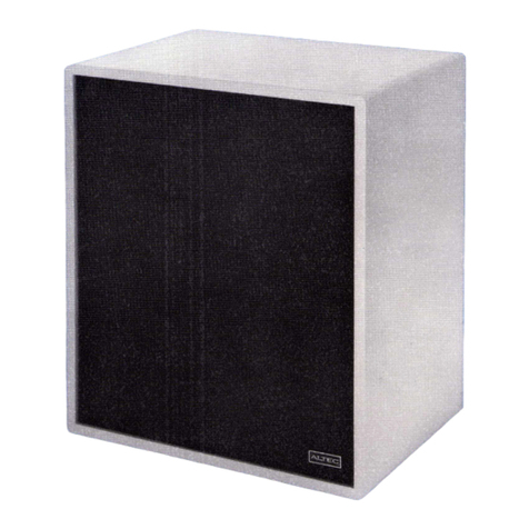
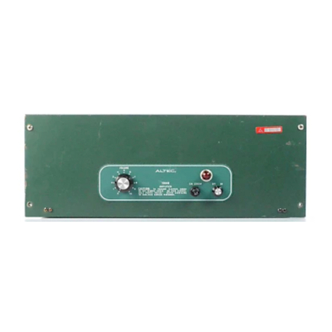
Altec Lansing 771B User manual

ALTEC. 771BAND771BX
ELECTRONICCROSSOVERBIAMPLIFIERS
OPERATING
INSTRUCTIONS
ALTEC 7718 and 7718X Electronic Crossover 8iamplifiers improve power handling and reduce distortion without
requiring a high-power amplifier and separate crossover network.
FEATURES:
Electronic Crossover with
Separate Power Amp Iifiers
Heavy LF Demands Do Not
Affect HF Performance
Full Amplifier Power and
Efficiency
Versatile Input Connections
Fail-Safe Protection for Output
Transistors
Export Model
ALTEC.
These ALTEC biamplifiers include electronic crossover circuitry and separate
low-frequency (LF)and high-frequency (HF) amplifiers ina single, compact
package that can be mounted directly in the speaker enclosure. The elec-
tronic crossover circuit divides the input signal into separate bass and treble
channels. A 60-watt LF amplifier drives the bass speaker and a 30-watt HF
amplifier drives the horn-loaded compression driver.
Extreme LF power demand does not affect HF reproduction because separate
amplifiers drive the LF and HF spea kers.
The electronic crossover is placed ahead of the dual power amplifiers so that
ful I biampl ifier output is distributed to the speakers.
Standard input connections are direct coupled. Transformer isolation of the
input is accomplished with an optional plug-in transformer. Input inter-
connecti9n phono jacks (7718 on Iy) permit connecting up to 20 biampl ifiers
into a single sound system.
ALTEC's Active Dissipation Sensing Circuit provides faiI-safe protection for
the output transistors. The action of the sensing circuit is immediate and
effectiveat all frequencies within the passband of the biamplifier, limiting
only that portion of the program material thatwould damage or degrade the
performance of the output transistors.
The ALTEC 7718X 8iamplifier (export model) is similar to the 7718, except
that voltage selection and fusing is provided for primary power. The jack for
connecting two or more biamplifiers into multiple systems is not provided.
Specifications and components subject to chang e without
notice . Ov erall performanc e will be maintain ed or improved.
1515 S. Manchester Ave., Anaheim, Calif. 92803 42-02-042741-01
Litho in USA CP-472-2.5K

Item
Title, Photograph and Description.
SPECIFICATIONS
OPERATION .
CONTROLS . • • • • •
NORMALCONTROL SETTINGS
VENTILATION. • • • •
USING INPUT TERMINALBOARD
OPTIONAL PLUG-IN TRANSFORMER
ACCESSORIES. • • •
CONNECTING 771Bs IN MULTIPLE
SYSTEMS • • • • • •
INSTALLATION . . .
SERVICEAND MAINTENANCE
INSTRUCTIONS. .
ACCESS
Installing Plug-In Input Transformer
Accessories • • • • • •
Power Driver Bias Adjustment •
PCBReplacement
RECOMMENDEDSERVICETECHNIQUES
Transistor Orientation.
Replacing Power Transistors .
Testing Transistors •
Replacing PCBComponents .
Repairing Fractured or Damaged PCB
Conductor . • •
PARTSLIST
MAIN CHASSIS •
LFPOWERDRIVERPCBASSEMBLY
HF POWERDRIVERPCB ASSEMBLY •
CROSSOVERPCBASSEMBLY •
DATA CONTENTS
Page
3
4
4
4
4
4
6
6
6
7
8
8
8
9
9
9
9
10
10
10
16
16
17
18
19
-2-
Graphics
771BCover Photograph . .
Table I. Operating Controls and Features
Figure No.
]. Controls and Features
2. Speaker Hookup and 771B
Interconnections. .
3. Biamplifier Interior . .
4. Typical Solid-State Component
Configurations . .
5. Power Transistor Installation
6. Schematic, 771B Electronic
Crossover Biamplifier
7. Schematic, 771BX Electronic
Crossover Baimplifier
8. Electronic Part Locations, LFPower
Driver PCBAssembly . . .
9. Schematic, LF Power Driver
PCBAssembly . . . .
10. Electronic Part Locations, HF Power
Driver PCBAssembly
11. Schematic, HF Power Driver
PCBAssembly . . .
12. Electronic Part Locations,
Crossover PCBAssembly . .
13. Schematic, Crossover PCB
Assembly . . . .
Page
1
. . 4
. . 5
. . 6
. 8
9
10
. 11
. 12
. 13
13
. . 14
. 14
. 15
. 15
-~ J

SPECIFICATIONS
Type:
Gain (with Full
Boost) -
Biamplifier with electronic cross-
over
BassAmplifier: 52 dB with 15356 Line Matching
Transformer
66 dB with 15095 Line Matching
Transformer
Treble Amplifier: 49 dB with 15356 Line Matching
Transformer
Input Sensitivity
(for Rated Output
with Fu11Boost):
Power Output -
BassAmplifier:
Treble Amplifier:
TotaI Harmonic
Distortion (THD):
IM Distortion:
Crossover
Frequency:
Frequency
Response:
Input Impedance:
Load Impedance:
Damping Factor:
Noise Level:
Controls:
63 dB with 15095 Line Matching
Transformer
0 .5V rms direct
0 .5V rms with 15356 Line Match-
ing Transformer (high-level ba 1-
anced-l ine matched input)
0. lV rms with 15095 Line Match-
ing Transformer (high-level bal-
anced-line matched input)
60 watts at less than O.5% THD
30 watts at less than O.5% THD
Less th a n O.5% at rated power,
20 Hz to 20 kHz
U n mea s u r a b Ie by norma I IHF
method
500, 800 or 1500 Hz with -12 dB/
octave slope
±1 dB from 20 Hz to 20 kHz (nor-
malized composite output)
80,000 ohms direct
600 ohms with 15356 or 15095
transformer
8ohms nominal foreachamplifier
25
80 dB below rated output
1 BASS GAIN CONTROL, con-
tinuously variable, +6 dB to -15
dB
1TREBLEGAIN CONTROL, con-
tinuously variable, +6 dB to -15
dB
- 3 -
Controls (Cont'd): 1 ELECTRON IC CROSSOVER
FREQUENCY switch, 500 Hz/800
Hz/1500 Hz
1 POWER switch
1 PRESS TO RESET pushbutton
(circuit breaker). Model 7718
only.
1 VO LTAGE SELECT switch.
Model 771BX only.
Power Requirements: 120V,50/60Hz,90watts. Model
771BX only.
Dimensions -
Overall:
Panel Cutout:
Weight:
Color:
Accessories:
Selectable 95V to 240V, 50/60
Hz, 90watts. Model 771 BXonly.
6-1/2" H x 9-7/8" W x 9" D
5-1/2" H x 9-1/2" W
16 pounds
Black
ALT EC 15095 Line Matching
Transformer (high-level balanced--
line matched input)
ALT EC 15356 Line Matching
Transformer (high-level balanced--
Iine matched input)
.-------NOTE --------.
IAccessories MUST BEORDERED SEPARATELY.1
INSTALLATION HARDWARESUPPLIED
6 -screws, 8-32" x 1-1/4"
6 - 'T' nuts, 8-32"
1 - Cable, 25 feet with phone plugs
4 - Speaker connecting wires with push-on
connectors

OPERATION
CONTROLS
VENTILATION
Al Inorma Ioperating controls and input jacks are located
on the front panel (see Figure l). Descriptions and
functions of controls and connections are Iisted in
Table I.
Air must circulate freely past the front panel of the bi-
amplifier for best performance. When moving or posi-
tioning the speaker enclosure containing the biampl ifier,
be sure free circulation of air past the heat-dissipating
vanes is not restricted by curtains, furniture, walls or
other equipment. Allow at least two inches of space in
front of the vanes.
NORMAL CONTROL SETTINGS USING INPUT TERMINAL BOARD
Recommended initial settings of the BASSand TREBLE
GAIN CONTROLS are at OdB. Adjust sound-system
volume at mixer/amplifier or other input device, then
use the BASS and TREBLEGAi N CONTROLS to boost
or attenuate the low and high frequencies for desired
resu Its.
The INPUT terminal board (see Table I and Figure l)
permits either direct coupling or transformer isolation
of the input. For direct coupling, connect the input
leads (shielded conductor recommended) to terminals l
and 2; terminal 2 is ground. For transformer-isolated
Table I. Operating Controls and Features
Item Name Function/Description
l BASS and TREBLE Provide separate control of bass and treble portions of input signal. Each
GAi N CONTROL control is continuously variable from +6 to -15 dB. Raise controls for gain,
potentiometers lower controls for attenuation. Controls are Iinear, slide-type potenti-
ometer.
-z FROM MIXER Connects (direct coupling) input signal from mixer, preamplifier or other
PREAMPLIFIER input device. Model 771B can accept an input signal from another 771B
jack for 771A).
3 INPUT Provides alternate direct coupling of input signal. Transformer isolation of
terminal input signal may be obtained when an optional ALTEC plug-in transformer
board accessorv is used.
4 TO ADDITIONAL Connects another 771B in parallel to enlarge the sound system.
POWER SPEAKER
iack
5 POWER switch Applies primary power. Pilot light in switch (771B only) is lit when power
is on.
6 PRESSTO Restores primary power if protective circuit breaker is open (771B only).
RESET If circuit breaker opens repeatedly, cause should be corrected before
pushbutton resettina.
7 VOLTAGE Must be set to appropriate voltage range before turning on amplifier
SELECT (771BX only). Selects proper transformer primary configuration for line
switch voltages of 95 to 240V, 50/60 Hz.
CAUTION
Turning switch with primary power applied to
amp Iifier may damage or burn out switch.
8 30 WATTS - 60 WATTS Connect HF and LF speakers. Terminals accept push-on connectors
speaker terminals without solderina.
9 ELECTRONIC Selects 500, 800 or 1500 Hz crossover frequency according to optimum
CROSSOVER requirements of speaker system.
FREQUENCY
switch
- 4 -
··~

Model 7718
Model 771BX
Side and Rear View
Figure 1. Controls and Features
- 5 -

coupling, connect the inp ut leads to termi na ls 3a nd 4.
Transformer-isolate d coup ling also requires insta llation
of a p lug-in ALTEC trans former accessor y.
OPTIONAL PLUG- IN IN PUT TRANSFORME RACCES-
SORIES
The ALTEC 15356 and 150 95 Line Matching Trans fo rmers
prov ide a high-level bala nced input capab il ity for th e
biam p lifier. The 15356 has a 0.5V rms inpu t sensit ivity
for full rated biamp lifieroutput. Input sensi ti v ity with
the 15095 is O. lV rms for full rated outpu t.
NOTE
THE ALTEC 15356 AND 15095 TRANSF ORM -
ERS ARE NOT CUSTOMER SERVICEABLE
COMPONENT S AN D THEREFORE MUST BE
INSTALLED BY AN ALTEC QUALIFIED SER-
VICE REPRESENTATIVE.
CONNECTING 771Bs IN MULTIPLE SYSTEMS
Each 771 B is pro vided wit h an interconnecti ng cab le to
combine an additiona I 77 1B into the sound syste m . Up
to 20 of the 771 Bs may be connected into a sing le sound
system in this mann er. Speaker hookup and parallel
mult iple-s ystem inter conn ections are shown in Figure 2 .
The input signal cab le i~ plugged into the FRO M MIXER
PREAMPLIFIER jack . The next 771 B is co nnected in
parallel by plugging the prov ided interconn ec ting cable
into the TO ADDITION AL PO WER SPEAKER jack on
the first 771 Band into th e FROM PREAMPLIFIER jack
on the second 771B . Co n t inue this int ercon nection
method to combine as man y 771Bs as requir ed (up to 20
units).
USE CABLE PROV IDED WITH EACH
771B BIAMPLIFIER TO CONN ECT
UP TO 20 UN ITS INTO THE SOUND
IN PUT SIGN AL FROM SYSTEM
MI XER, PREAMPLIFIER, / \
ETC.
,--+--
--~ ·~-
-- 7
I
I
I
I
I
LINE I
POWERI
771B
BIAMPLIFIER
COM HF COM LF I
I
I
§ I
I
I
I
I
I
771B
BIAMPLIF IER
COM HF COM LF
I LIN E
§ I POWER
I
I
I
I
I
L - _:l'~~E ~L::: U.'.:.:. - _J
Figure 2 . Speak er Hookup and 771 B lnt ercon nec tios
INSTALLATION
The 7718 and 771BX are designed to be installed at a
convenient location int he speaker enclosure. If in-
stallation is made in an ex isting spea ker system, the
passive crossover net work a Iread y pre sent in the system
must be remo ved because the biam p lifier contains an
electronic crossover c ircu it.
If the biamp lifier is to be installed in an enclosure not
previousl y prepared for its installat io n, complete all
steps of the fol lowing procedure. If the biamplifier is
to be install ed inan ALTEC enclosure specificall y pre-
pared for it, complete onl y Steps 5, 6 and 7 of the in-
stallation procedure.
Step 1. Cu t rectangular hole 5-1/2 " high b y 9- 1/ 2"
wide in enclosure at desire d location. Note
required dep th to accommo da te biampl ifier is
9" .
Step 2 . Insert biamplifie r in cutout a nd mark center
po ints for each of six hole s to be drilled fo r
se curing hardware . Remov e bi amp Iifier.
Step 3 . Use 7/ 32" (0.218") to dri 11 and bore holes,
loca ted in Step 2, toaccep t shaft of 8-32" 'T'
nuts supplied with biamplifi er . Remove debris
from enclosure and edges of holes.
- 6 -
Step 4 . Inser t six 'T' nuts in mounti ng holes from inner
side of enclosure. Gently h ammer each in
place until 'T' nut faces ar e flush with enclo-
sure surface .
Step 5. Install suppl ied speakerwir es on speakers and
biamplifier speaker termina ls (see Figure 2).
Note that minimum speaker impedance is eight
ohms .
Step 6 . Verif y that ELECTRONIC CROSSOVER FRE-
QUENCY switch is set to appropriate 500,
800 or 1500 Hz posit ion, as requ ired by speaker
system.
Step 7. lnsertbiamplifie r incutouta nd secure it to 'T'
nuts with si x (6) 8-32 " x l-1/4''screws
(supplied) .
SERVICEAND MAINTENANCE
INSTRUCTIONS
This service information is for the use of authorized warranty stations (dealers) only. Service must be
performed by an ALTEC Qua Iified Service Representative.
NOTICE
REPAIRPERFORMEDBYOTHERTHAN AUTHOR-
IZED WARRANTY STATIONS (DEALERS)OR
OTHER QUALIFIED PERSONNELSHALLVOID
THE WARRANTY PERIODOF THIS UNIT. TO
AVOID LOSSOFWARRANTY,SEEYOUR NEAR-
ESTALTEC AUTHORIZED DEALER OR CALL
ALTEC CUSTOMER SERVICE DIRECTLY AT
(714) 774-2900, OR WRITE:
Customer Service
ALTEC
1515 South Manchester Avenue
Anaheim, California 92803
- 7 -

ACCE SS
Remove thee igh t scr ewsse curing the cove r to the cha ssis.
Care fully slide co v er off , fle x ing it sligh tl y to clear
the scre ws that atta ch the speaker terminal brac ket.
lnstal ling Plug-In Input Transformer Acces sorie s
Veri fy line power is turne d off, th e n rem ove chass is
co ver. Carefu 11y pIug the accessor y inpu t tran sformer
into the octal socket (J3) in the chas sis (see Fig ure 3) ,
then replace chassis cover and secure with eight screws
prev iously removed .
Power Driver Bias Adjust ment
Adjustment of the power driver bias control (s) ma y be
required when repl a cing a p o w er transisto r or power
dri ver printed circuit boa rd (PCB) . One bias adjus ting
cont rol is located on each powerdri ver PCB; R12o n the
HF power drive r PCB and R13 on the LF po w er dr iver
PCB (see Figures 3 and 9) . These con trols set the bias
for proper crossover between negativ e and positive sig-
nal components of power transistors Ql an d Q2 (HF);
Q3 and Q4 (LF) (see Figures 3 and 5) . Imprope r ad-
justment of these controls resu I ts in disto rti on a t the
crossover frequenc y. To adjust either Rl 2 or R13, use
the fol lowing procedure:
1. Verif y Iine power is turned off, then remove chassis
cover .
2. If adjus ting R12, se t a de VTVM to scale that will
conven iently read 20 mV and co nnect its positive
(+) lead to Q 1emitter and its negat ive (-) lead to
Q2 co llector (see Figure 4, Motorola MJE).
3. If adju st ingR 13, set a dcVTVM to scale that will
conveniently read 20 mV and co nnect its positive
(+) lead to Q3 emitter and its negative (-) lead to
Q4 col lector (see Figure 4, Motorola MJE).
4 . Turn on line power to biamplifi er .
5 . Observ e VTVM; it should read a ppro x imately 17 .5
mV.
6 . Adjust bias control (R12 or R13) , as necessary(see
Figure 3). Cloc kw ise adjustment increases voltage,
counte rc lockwise adjustment de creases voltage.
7. Allow stabili zation 15 to30minu tes for drift check .
If de vol tage reading changes more than ±15 mV,
readjus t bias control for 17.5 mV .
8 . Turn off line power, disconne ct VTVM, replace
chassis cover and secure with e ight screws previ-
ous Iy removed .
Fig ure 3. Biamplifier Interio r
- 8 -

PCBReplacement
A crossover PCBand twopower driver PCBsare located
within the chassis (see Figures 3 and 6). Use the fol-
lowingprocedure to replace a failed PCBwith a new or
repaired PCB.
1. Verify line power is turned off, then remove chassis
cover.
2. If a power driver PCBis being replaced, carefully
remove cable connector from jack on PCB.
3. Carefully remove PCBfrom standoffs, loosening
evenly at each corner.
------CAUTION------
Do not warp, bend or twist the board or con-
ductor may fracture.
4. Carefully press new or repaired PCBinto place on
standoffs. Presscorners in place evenly until
plastic fasteners lock PCB in position.
5. If a power driver PCBis replaced, carefully press
cable connector, previously removed, onto jack on
PCB. Verify that power driver bias adjustment is
correct and readjust if necessary. Refer to Power
Driver Bias Adjustment procedure.
6. Replace chassis cover and secure with eight screws
previously removed.
RECOMMENDEDSERVICETECHNIQUES
If systematic troubleshooting shows need for parts re-
placement, observe the fol lowing precaustions.
Transistor Orientation
Solid-state components are packaged in various case
sizes and types with various lead orientations (see Figure
4). Before removing a solid-state component from tie
points or from a PCB, sketch the lead orientation with
respect to the tie points or PCB.
Formthe leads of the new component to conform with
the leads of the part being replaced to aid in making
proper connections.
Beforeremoving small transistors, note position of index
tab with respect to the PCBor socket. Cut the leads
of the new transistor to the required length and insert
(""' them into the PCBor socket properly indexed.
Replacing Power Transistors
Besure the following conditions exist when replacing
power transistors.
-9-
T0-5
Lead 1 - Emitter
Lead 2 - Base
Lead 3 - Collector and Case *
£Index Tab
* Not all types. Some have base-to-case
internally; others have no connection
to case.
G .E. Epoxy
Lead E - Emitter
Lead C - Collector
Lead B - Base
T0-92 .
Lead E - Emttter
Lead B - Base
C Lead C - Collector
Motorola MJE
(D 2
D 3
D) Lead 1 - Emitter
Lead 2 - Collector
Lead 3 - Base
"'-- Heat Sink Contact
Area(Bottom)
Figure 4. Typical Solid-State Component
Configurations
1• The mica insulator is not damaged. If damaged,
use new insulator.
2. No grit or meta I particles are between replacement
transistor and heat sink.
3. Bothside of mica insulator are covered with silicone
grease or fluid.
4. Mounting screws are tight (see Figure 5).
------CAUTION------
1nst a 11 concave washer on power trans istor
with concave surface DOWN; otherwise,
power transistor may fracture.

CONCAVE WASHER
(INSTALL WITH CONCAVE SIDE DOWN)
l r
MOUNTING SCREW
POWER TRANSISTOR
i HEAT SINK
~=;1,~
Figure 5. Power Transistor Installation
Testing Transistors
Transistors should be checked with a transistor tester.
If a tester is not ava i(able, use the following procedure
for testing transistors with an ohmmeter.
Step 1. Remove suspected transistor from circuit (see
Replacing PCBComponents).
Step 2. Connect ohmmeter leads to base and emitter.
Read on lowest ohms sea le. Reverse leads and
read again. Normal readings sh o u Id be at
least 10 times greater in one direction than in
the other.
Step 3. Connect ohmmeter leads to base and collector
and repeat Step 2. Ohmmeter readings should
be similar to those obtained in Step 2.
Step 4. If Steps 2and 3 show normal function,connect
ohmmeter leads to col lee tor and emitter. Read
on lowest ohms sea le. Reverse leads and read
again. If reading is low and virtually
unchanged when ohmmeter leads are reversed,
the transistor has a short circuit between col-
lector and emitter.
Replacing PCBComponents
The main ch ass is schematic for the 771B is shown in
Figure 6 and the main chassis schematic for the 771BX
is shown in Figure 7. Component locations on the PCBs
are shown in Figures 8, lOand 12. PCBschematics are
shown in Figures 9, 11 and 13. Before removing PCB
components for testing or replacement, read and heed
the fol lowing instructions.
- 10 -
1• Solid-state components and PCBsmay be damaged
by excessive heat. Use a small soldering iron with
a 1/8-inch diameter chisel tip. Use small-diam-
eter, 60/40 rosin-cored solder.
2. Remove components by placing soldering iron on
component lead on conductor side of PCBand pull
out lead. Avoid overheating the conductor.
-----CAUTION--------.
The conductor on the PCBis a metal sur-
face plated with solder and laminated to
the board. Too much pressure or over-
heating may Iift the conductor from the
board.
3. Ifcomponent is faulty or damaged, clip leads close
to component and then unsolder leads from board.
Withdraw leads from component side.
4. Clear so Ider from circuit board holes before in-
serting leads of new component. Heat solder re-
maining in hole, remove iron and quickly insert
a pointed nonmetallic object, such as a toothpick
from conductor side.
5. Shape new component leads and clip to proper
length. Lead shape should provide stress relief for
component. Insert leads in holes, observing same
polarity or orientation of removed component.
Apply heat and solder on conductor side.
Repairing Fractured or Damaged PCB Conductor
If a conductor is fractured, damaged or Iifted from the
circuit board, a recommended method of repair is to
solder a section of good conducting wire along the
damaged area and seal with epoxy.

~
iA17
I CRii~~~R-- I
JI -o---.--,;----------..·,------, >6 4d, · ·
1
27-01-042638 TAEBLE
•
~
>5 , <l;.,______J l l~o'.
J2
INPUT
TB9
'2. CAPACITORSAAE GIVEN IN MICRO-FARADS
I
'
'
CB
,01
Tl
745S
0-----4---~
I I I
L __ _;_i
I, RESISTOR VALUES ARE GIVEN IN OHMS l/4W I 10":i
NOl'ES:UNLESSOTHERWISEINDICATED.
l ;j_____,
I
I
L____j
CAI
SCBAI
r---
,---,. I ,+201/
CA4
3A200
CA,5
+85V
, BASS
.Al
10K
R2
IK
+52V
3A200
+ Cl
~~,5'0c~
6200
75V
+ 1~3
5000
60V
-~-~.:::I
,
::,~f.:E~+52V
I QP.IVER~~7(1~~1----- ,...J.,J
I27-~~t~~456(1;....p , It"'
11:!" S(i
1- 4(:~-:r11 J"" I
I
: :~~--,-,ff
rl
: 7 8(1
L_ --~
~
F.~~E~
DAIi/EA
BOAP.O 7
I 27-0t-042244
I 6<1-----t--,---\I
'
jE----------1-----+-+-I-
~
><j ·~""ff
I c!:
L_~· C7
p7
AIO
5
5W
N,1. Al2
2.2K
l/2W
TB1J
H, F,
L.F.
L.F. COM
H.F. COM
Figure 6. Schematic (3D212-1), 771B Electronic Crossover Biamplifier
eu i:=oa. f'2oo
SCHEMATIC,
Bl-AMPLIFIER
,~
&Ill.
A--'Nr?Wt...,A4M:.IJ>c.
ANAHlr ..... CAUPOftNIA.
DI3D?\2.-1
IHHT ! M!

I',.)
j-Al7 ,-A2-
JI
I CRi~rft~R-- I : H.F.POWER /
1
21-01-042638 TREBLE I DRIVER 7( ~-+ ,_s~2v______ __,
- I - BOARD I I
-o---+--0,----------.s,- T-- )>6 'I( - ' 27-0t-042245 F4AMP
)5 ><I<------' 03 WI ·~ I
I "I,-----~ ,oK :1J1 s11
INPUT
TB9 .
Q)I , ,~
5'/.
"
7 5 4 3
Tl
WHTfBll.ll
15 V
I AMP 115 V
F4 WIIT/ iUO:
IAMP 115V
W~T{Ol!IJ
r/7
Pl
I
I 2<1- ~: 1-=- 4<1<- - +------ - --+--; f-~ .- -- -,
I I R9
: I 3~f---!--- - ----- iw
I I 2<<-- +----+-----c-cH it TN.I.A.JI
1 , • 2;ffw
I _r-:-<'
I 1 - ~/
I . _I -
L___ __lJ l__ __•
, BASS
Al
!OK
R2
IK
~F.~E~
OAIVER
BOA.P.D 7
: 27-0l -042244
G<!f--'--------j- , --\1,
j
-------+--+-i ·
~
CA4 +85V
,.:Jol I +S2V
CR-5
-.i----
3A200
+ Ic1 c2l.+ ..l{:3
~~oo620 0TTsooo
V 75V 60V
"I
L_:j '-- C7
p7
Al2
2.2K
112w
TBII
H.F.
L.F.
L. F. COM
H.F. COM
_,...............,...
QI ' f t':L 1%:i2. ~OP °Sft>1i. 'fl•
HIGHEST l1G:FERENCE DE.51GNATl0N USEO
Al2 CB CAIi 04 Tl
52 A3 P3 ,.
REFERENCE OESlGNAil ONS NOT USED
I I I
•.... . ..•~•••·••.....C• HL 1;,o;,.~~'j~ SCHEMAT IC,
771BX B~AMPU FIER ALTEC.
3 3Wli(H s;- ':iHOWrJ IN ')''.,/10 ~ '05 ITIC'~; A('T,\T IC'N CY.
2. CAPACITOAS ARE GIVEN IN MICr-()-FARAOS
I, AES ISTOA VALUES ARE GIVEN IN OHMS 1/4W ::t IO'"Al
NOTES, UNLESSOTHERWISEINDICATED.
Figure 7 . Schematic (3D228-1), 771BX Electronic Crossover Biamplifier
771
~
IK•~--1<=
,.__,,,a. ~ U-.A............
,. .. .... . ,.. .c:-. ..... ...... ,,.
Dl3D22e- 1
•"n ·, I Cl_l

0
~
:
0~~$~
E
CJ
CJ
CJ
CJ
C ) c(8
$~~:::~~!!B
~~~$·~,
+
M
u
M
u
0
~
-....--- + C4
SELECTED RESISTOR
1/4 WATT!11.PER L.F.
POWERDRIVER BOARD
PRODUCTIONTEST
PROCEDURE
Figure 8. Electronic Part Locations (2C573-4), LF Power Driver PCB Assemb!y
JI jc°'oov
R32 RI
IK 18K
f-
C,4
470Pf
+ CZ R3
R30
4,7K
R4
20 R7
100
C3
5 50V
r---------------< J2-B
r----.--------+-------------~B+ J2-7
C5
,47
R9
18K
RIO
47K
R29
330 CR2
IN456A
Rl4
10
04
41440 C9
,47
Rl7
100 CIO
~7
07
39390
R26
I 0
CII
,01
4
IN456A
CR5
IN 6A
R27
100
R20 R23 + Cl3
4.7K 2.2K 50/SOV
Cl2
.01
R24
120
CR7
TA·IO
J2-6
J2-5
OUTPUT JZ- 4
CR6
TA-10
50/SOV
~~
~-----+-~-----+--------;-------t------+-------<GNO JZ-I
'-----c,----------t----+-----------< J2-10
~----+----------< J2-9
Figure 9. Schematic (2D544-7), LF Power Driver PCB Assembly
- 13 -
+
N
u
0
lO
u
0

Ji
0
CJ
E
c(8
B
(TYP)
0 $·$
~
-@]- + C4
RI
33K
R2
IOK
+ CZ R3
z!j.lsov10K
Figure 10. Electronic Part Locations {2C572-3), HF Power Driver PCBAssembly
RS
3.3K
R6
3.3K
CRI
TAIO
R4
470
s7:ov
C4
2~0V
cs
117
+ C6
50/5
BIAS
ADJ.
+ C7
5/SOV
39390
r~i
l/2W
RII
18K
l/2W
Rl2
500
CRZ
TAIO
,------+--+------<8
Rl4 Rl9
3.3K 100
5% OUTPUT 4
CR3
TAIO
GND I
'---------------<9
Figure 11. Schematic (20545-4), HF Power Driver PCBAssembly
- 14 -
0
#-.,e5T ,e,FP J)e5,d,M4710/l'SU5ED
~B I a.e.:!fl I ..T/ I ,,,ezo
I I I
IA!="'P"e.E'S~ ~M477dA/!SA4:/T4>1Z,
I I I
I I I ."""'

(""
+
INPUT
6
r:-GND
5
+
C4
Cl
5
25V
+
C2
5
25V
RI
IMEG
+
ClO
R2
IOOK
R3
IOOK
R4
220K
+
C9
0 0
S1
0 0
+
C2
D D D D D
,..
,~
cs
D
,,
,,
+
+
C3
Cl
,,
....,
ca
,,
....~
Figure 12. Electronic Part Locations (3C065-l), Crossover PCB Assembly
+
C3
50
50V
+
01
AL
41627
RS
3.3K
B+ 7
R20
IK
51-C + L.F. OUT
t--<2
C9
25
25V
5,r. cs
R7
18K
57.
C4
25
25V
.012
57.
RIG
4.7 K
Rl7
22K
Rl4
39K
57,,
C6 21 C7 • H.F. OUT
.012 33K •012 t----(4
5'1, 5% 57.
R9 RII CIO
25
ISK 18K 25V
57, &% 10
S I-B 9
RG 7 8 Rfq
22 K
HIGHEST-REFERENCE D-ESIGNATORUSED
R24 I CID I 03 I 51 I
I I 7 I
4,7K 8 GNO REFERENCE DESIGNATION NOT USED
R 15
3
GND
Figure 13. Schematic (3C066-2), Crossover PCB Assembly
-15 -
IR 18
I I I I
I 7 7

Reference
Designator
Al
A2
A3
Cl
C2
C3
C4
cs
C6,7
CB
CBl (771B
only)
CRl
CR2,3,4,5
PARTSLIST
771B/771BXMAIN CHASSIS
Ordering
Number Name and
Description
27-01-042638-01 PCBassembly, cross-
over
27-01-042245-01 PCB assembly, HF
power driver
27-01-042244-01 PCB assembly, LF
power driver
15-01-100296-01 Cap., 5000 >,iF,25V
15-01-107511-01 Cap., 6200 >,iF,75V
15-01-100298-01 Cap., 5000>,iF,60V
15-01-100279-01 Cap., 500>,iF, 50V
15-01-114352-01 Cap., 4000 >,iF,50V
15-06-102605-01 Cap., 0.47 >,iF±10%,
lOOV
15-02-100089-0 l Cap. , 0. 0l >,iF±20%,
4000V
51-03-109809-02 Circuit breaker,
2.2A hold, 3.25A
trip
48-02-108577-01 Diode bridge recti-
fier, 1.5A, 100 PIV
48-02-107467-01 Diode, rectifier,
1N5402, 200V, 3A
Reference
Designator
J3
Ql ,2,3,4
Rl,3
R2,4
R5,7
R6,8
R9, 10
Rll,12
(771BXonly)
R13 (771BX
only)
Sl (771B
only)
S1 (771BX
only)
S2(771BX
only)
Tl (771B
CR6,7,9,10 48-01-109275-01 Diode, Zener, only)
Tl (771BX
CR8, 11
F1,2
F3,4 (771BX
only)
Jl
J2 (771B
only)
1N746, 3 .3V ±10%,
400 mW
48-01-107429-01 Diode, stabistor, 3-
pellet
51-04-100462-0l Fuse, 1/4A, 3AG,
250V
51-04-100464-01 Fuse, lA, 3AG
21-01-114347-01 Jack
only)
TB9
TBl1
Wl ,2
- 16 -
Ordering Name and
Number Description
21-02-100973-01 Socket, octa I
48-03-109715-02 Transistor
47-06-042269-02 Pot., 1OK0, Btaper
47-01-102163-01 Res., 1KO±l0%,
1/4W
47-02-107434-01 Res., 0.330 ±10%,
3W
47-02-108238-01 Res. , 0. 25 0 ±10%,
3W
47-02-112166-01 Res., 5 0 ±10%, SW
47-01-102359-01 Res., 2.2K 0±10%,
1/2W
47-01-102075-01 Res., 750 0 ±5%,
1/4W
51-02-113986-01 Switch assembly,
DPDT, w/pilot lamp
51-02-113535-01 Switch, SPDT, slide
51-01-042617-01 Switch, 2-gang,
rotary
56-08-007458-01 Transformer, power
56-08-007543-01 Transformer, power
21-04-101038-01 Terminal board, 4-
terminal, input
21-04-030799-01 Terminal board, 4-
terminal, speakers
60-09-042284-02 Cable assembly

PARTSLIST(continued)
LFPOWERDRIVERPCBASSEMBLY
Reference Ordering Name and
Designator Number Description Reference Ordering Name and
Designator Number Description
Cl 15-01-107452-01 Cap •, 10µF, 50V
C2,6, 13 15-01-100241-01 Cap., 50 µF, 50V
C3,7 15-01-110771-01 Cap., 5µF, 50V
R5,6 47-01-102169-0l Res., 3.3K 0±10%,
l/4W
R7,16, 17
C4 15-01-107500-01 Cap., 100 µF, 50V
C5,9, 10 15-06-108173-01 Cap., 0.47µF±20%, 25,27 47-01-102151-0l Res., 1000 ±10%,
l/4W
100V
ca 15-02-107454-01 Cap., 100 pF±10%, R8 47-01-102067-01 Res., 360 0 ±5%,
l/4W
100V RlO 47-01-102183-01 Res., 47K O ±10%,
Cl 1,12 15-02-100307-01 Cap., 0.01 µF, ±20%, l/4W
100V
C14 15-02-100302-01 Cap., 470 pF±10%, Rll,12 47-01-102359-0l Res., 2.2K 0±10%,
l/2W
100V R13 47-05-107504-0l Pot., 500 0 ±20%,
CR1,2,3,4,5 48-01-107017-01 Diode, 1N456A, 2W
25V, 100 mA Rl4 47-01-102140-01 Res., 10 0 ±10%,
CR6,7 48-01-102592-01 Diode l/4W
CR8 48-01-110786-01 Diode, Zener, 23V Rl5 47-01-102147-01 Res., 47 0 ±10%,
±5%, 2W l/4W
Jl 21-01-109731-01 Jack, phono Rl8,19,
Ql,2 48-03-110773-01 Transistor, PNP,50V 20,30 47-01-102171-01 Res., 4.7K 0±10%,
Q3,7 48-03-107447-02 Transistor, 2N5320, 1/4W
NPN, 10W, 75V R21 47-01-102156-0l Res., 270 0 ±10%,
Q4 48-03-041440-01 Transistor, PNP l/4W
QS 48-03-101098-01 Transistor, NPN R22,23 47-01-102167-01 Res., 2.2K 0±10%,
Q6 48-03-107448-02 Transistor, 2N5322, l/4W
PNP, 1OW, 75V R24,26 47-01-102152-0l Res •, 1200 ±10%,
Rl,9 47-01-102178-01 Res., 18KO ±10%, 1/4W
l/4W R29 47-01-102157-01 Re s •, 330 0 ±10%,
R2 47-01-102181-01 Res., 33K O ±l0%, 1/4W
l/4W R31 47-01-000001-01 Res., value specially
R3 47-01-102116-0l Res., 39K O ±5%, s e Ie ct e d in test ,
l/4W ±5%, l/4W
R4 47-01-102155-01 Res., 220 0 ±10%, R32 47-01-102163-01 Res., lK O ±10%,
l/4W l/4W
- 17 -

PARTSLIST{continued)
HF POWERDRIVERPCBASSEMBLY
Reference Ordering Name and Reference Ordering Name and
Designator Number Description Designator Number Description
Cl 15-06-100311-01 Cap., 0.1 µF±20%, R1,8 47-0 l -102181 -0 l Res., 33K Q ±10%,
250V l/4W
C2,4 15-01-107501-0l Cap., 25 µF, 50V R2,3, 14,16 47-01-102175-0l Res., l0K Q ±10%,
C3,7 15-01-110771-01 Cap., 5 µF, 50V l/4W
cs 15-06-108173-0 l Cap., 0 .47 µF±200/o, R4 47-01-102159-0l Res., 470 Q ±10%,
lO0V l/4W
C6 15-01-10024 l -0l Cap., 50 µF 50V R5,6,15,17 47-01-102169-0l Res., 3.3K Q±l0%,
ca 15-02-107454-01 Cap., 100 pF±l0%, l/4W
l00V R7,21 47-01-102163-0l Res., lK Q ±10%,
C9 15-02-100302-0l Cap., 470 pF±l0%, l/4W
l00V
CRl,2,3 48-01-102592-0l Diode R9 47-0 l -102183-0 l Res. , 47K Q ±l0%,
l/4W
Jl 21-0 l-109731-0 l Jack, phono
Ql ,2 48-03-108557-02 Transistor, 2N5367, Rl0, 11 47-01-102359-01 Res., 2.2K Q±l0%,
l/2W
PNP, 0.36W, 40V
Q3,7 48-03-107447-02 Transistor, 2N5320, Rl2 47-05-107504-01 Pot., 500 Q ±20%,
2W
NPN, l0W, 75V
Q4 48-03-101098-01 Transistor Rl3,20 47-01-102156-0l Res •, 270 Q ±l0%,
l/4W
Q5 48-03-041440-0l Transistor
Q6 48-03-107448-02 Transistor, 2N5322, Rl8, 19 47-01-102151-01 Res., 100 Q ±10%,
l/4W
PNP, lOW, 75V
- 18 -

Reference Ordering
Designator Number
Cl ,2 15-01-108543-01
C3 15-01-100241-01
C4,9, 10 15-01-107495-01
C5 15-06-051240-02
C6,7,8 15-06-109091-01
Ql ,2,3 48-03-041627-01
Rl 47-01-100482-0l
R2,3 47-01-102187-01
R4 47-01-102191-01
R5 47-01-102169-0l
R6,17 47-01-102179-01
PARTSLIST(continued)
CROSSOVERPCBASSEMBLY
Name and Reference
Description Designator
Cap., 5JJF, 25V R7,ll, 12
Cap., 50 JJF, 50V
Cap., 25 JJF ±10%, R8, 10,21
25V
Cap., 0 .025 JJF±5%, R9
lO0V
Cap., 0.012JJF±5%, Rl3
lO0V
Transistor Rl4
Res., lM Q ±10%,
l/4W Rl6,19
Res., l00 KQ±l0%,
l/4W R20
Res•, 220K Q±10%,
l/4W R22,24
Res., 3.3K Q±l0%,
l/4W R23
Res., 22K Q ±10%,
l/4W Sl
- 19 -
Ordering Name and
Number Description
47-01-102108-01 Res • , 18KQ ±5%,
l/4W
47-01-102114-0 l Res., 33K Q ±5%,
l/4W
47-01-102106-01 Res., 15KQ ±5%,
l/4W
47-01-102123-01 Res., 68K Q ±5%,
l/4W
47-01-102116-01 Res., 39K Q ±5%,
l/4W
47-01-102094-0l Res., 4.7K Q ±5%,
l/4W
47-01-102163-0l Res., lK Q ±10%,
l/4W
47-01-102101-01 Res., 9. lK Q ±5%,
l/4W
47-01-102109-01 Res., 20KQ±5%,
l/4W
57-02-042698-01 Switch, slide, 4P3T
This manual suits for next models
1
Table of contents
Other Altec Amplifier manuals

Altec
Altec 1590B User manual

Altec
Altec 9440A POWER AMPLIFIER User manual

Altec
Altec 612C SPEAKER CABINET User manual

Altec
Altec 1612A SIGNAL PROCESSING User manual

Altec
Altec 1594B User manual

Altec
Altec 1567A User manual

Altec
Altec 1566A User manual

Altec
Altec 9440A POWER AMPLIFIER User manual

Altec
Altec 1612A SIGNAL PROCESSING User manual

Altec
Altec 1606A User manual