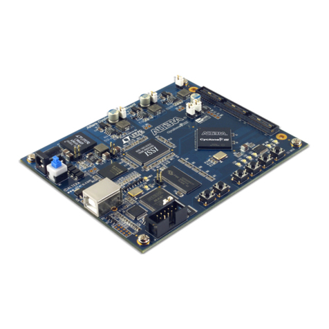
Altera Stratix IV GX User manual

Copyright © 2009 Altera Corporation. All rights reserved. Altera, The Programmable Solutions Company, the stylized Altera logo, specific device designations, and all other
words and logos that are identified as trademarks and/or service marks are, unless noted otherwise, the trademarks and service marks of Altera Corporation in the U.S. and other
countries. All other product or service names are the property of their respective holders. Altera products are protected under numerous U.S. and foreign patents and pending ap-
plications, maskwork rights, and copyrights. Altera warrants performance of its semiconductor products to current specifications in accordance with Altera's standard warranty,
but reserves the right to make changes to any products and services at any time without notice. Altera assumes no responsibility or liability arising out of the application or use of
any information, product, or service described herein except as expressly agreed to in writing by Altera Corporation. Altera customers are advised to obtain the latest version of
device specifications before relying on any published information and before placing orders for products or services.
UG-01060

© March 2009 Altera Corporation Power Delivery Network (PDN) Tool for Stratix IV Devices User Guide
Contents
Chapter 1. Power Delivery Network (PDN) Tool User Guide for Stratix IV Devices
Introduction . . . . . . . . . . . . . . . . . . . . . . . . . . . . . . . . . . . . . . . . . . . . . . . . . . . . . . . . . . . . . . . . . . . . . . . . . . . . 1-1
Application of the Tool . . . . . . . . . . . . . . . . . . . . . . . . . . . . . . . . . . . . . . . . . . . . . . . . . . . . . . . . . . . . . . . . . . . 1-1
PDN Decoupling Methodology Review . . . . . . . . . . . . . . . . . . . . . . . . . . . . . . . . . . . . . . . . . . . . . . . . . . . . 1-1
PDN Circuit Topology . . . . . . . . . . . . . . . . . . . . . . . . . . . . . . . . . . . . . . . . . . . . . . . . . . . . . . . . . . . . . . . . . 1-1
Major Tabs of the PDN Tool . . . . . . . . . . . . . . . . . . . . . . . . . . . . . . . . . . . . . . . . . . . . . . . . . . . . . . . . . . . . . . 1-4
BGA Via . . . . . . . . . . . . . . . . . . . . . . . . . . . . . . . . . . . . . . . . . . . . . . . . . . . . . . . . . . . . . . . . . . . . . . . . . . . . . 1-6
Plane Cap . . . . . . . . . . . . . . . . . . . . . . . . . . . . . . . . . . . . . . . . . . . . . . . . . . . . . . . . . . . . . . . . . . . . . . . . . . . . 1-7
Cap Mount . . . . . . . . . . . . . . . . . . . . . . . . . . . . . . . . . . . . . . . . . . . . . . . . . . . . . . . . . . . . . . . . . . . . . . . . . . . 1-8
X2Y Mount . . . . . . . . . . . . . . . . . . . . . . . . . . . . . . . . . . . . . . . . . . . . . . . . . . . . . . . . . . . . . . . . . . . . . . . . . . . 1-9
Library . . . . . . . . . . . . . . . . . . . . . . . . . . . . . . . . . . . . . . . . . . . . . . . . . . . . . . . . . . . . . . . . . . . . . . . . . . . . . 1-10
Decap Selection . . . . . . . . . . . . . . . . . . . . . . . . . . . . . . . . . . . . . . . . . . . . . . . . . . . . . . . . . . . . . . . . . . . . . . 1-13
BOM . . . . . . . . . . . . . . . . . . . . . . . . . . . . . . . . . . . . . . . . . . . . . . . . . . . . . . . . . . . . . . . . . . . . . . . . . . . . . . . 1-17
Design PCB Decoupling Using the PDN Tool . . . . . . . . . . . . . . . . . . . . . . . . . . . . . . . . . . . . . . . . . . . . . . 1-18
Pre-Layout Instructions . . . . . . . . . . . . . . . . . . . . . . . . . . . . . . . . . . . . . . . . . . . . . . . . . . . . . . . . . . . . . . . 1-18
Derive Decoupling in a Single-Rail Scenario . . . . . . . . . . . . . . . . . . . . . . . . . . . . . . . . . . . . . . . . . . . . . 1-19
Derive Decoupling in the Power-Sharing Scenarios . . . . . . . . . . . . . . . . . . . . . . . . . . . . . . . . . . . . . . . 1-22
Summary . . . . . . . . . . . . . . . . . . . . . . . . . . . . . . . . . . . . . . . . . . . . . . . . . . . . . . . . . . . . . . . . . . . . . . . . . . . . . . 1-24
Document Revision History . . . . . . . . . . . . . . . . . . . . . . . . . . . . . . . . . . . . . . . . . . . . . . . . . . . . . . . . . . . . . . 2-1
How to Contact Altera . . . . . . . . . . . . . . . . . . . . . . . . . . . . . . . . . . . . . . . . . . . . . . . . . . . . . . . . . . . . . . . . . . . 2-1
Typographic Conventions . . . . . . . . . . . . . . . . . . . . . . . . . . . . . . . . . . . . . . . . . . . . . . . . . . . . . . . . . . . . . . . . 2-2

© March 2009 Altera Corporation Power Delivery Network (PDN) Tool for Stratix IV Devices User Guide
1. Power Delivery Network (PDN) Tool
User Guide for Stratix IV Devices
Introduction
PCB designers must estimate the number, value, and type of decoupling capacitors
needed to develop an efficient PCB decoupling strategy during the early design
phase, without going through extensive pre-layout simulations. Altera’s Power
Delivery Network (PDN) tool provides these critical pieces of information. This
release of the PDN tool is specific to Stratix®IV GX devices.
fFor general purpose PDN tool information, refer to the Power Delivery Network (PDN)
Tool User Guide.
The PDN tool is a Microsoft Excel-based spreadsheet tool used to calculate an
impedance profile based on user inputs. For a given power supply, the spreadsheet
requires only basic design information, such as the board stackup, transient current
information, and ripple specifications to calculate the impedance profile and the
optimum number of capacitors to meet the desired impedance target (ZTARGET). The
tool also provides device- and power rail-specific PCB decoupling cut-off frequency
(FEFFECTIVE). The results obtained through the spreadsheet tool are intended only as a
preliminary estimate and not as a specification. For an accurate impedance profile,
Altera recommends a post-layout simulation approach using any of the available
EDA tools, such as Sigrity PowerSI, Ansoft SIWave, Cadence Allegro PCB PI, etc.
Application of the Tool
The purpose of the PDN tool is to help the design of a robust power delivery network
for Stratix IV GX devices by determining an optimum number, type, and value of
decoupling capacitors needed for selected device/power rail to meet the desired
ZTARGET up to FEFFECTIVE. This spreadsheet tool is useful for exploring the various what-if
scenarios during the early design phase, without extensive and time consuming
pre-layout analysis.
PDN Decoupling Methodology Review
This section describes general PCB decoupling methodology and explains in detail
the two parameters (ZTARGET and FEFFECTIVE) provided by the PDN tool for guiding PCB
decoupling design.
PDN Circuit Topology
The PDN tool is based on a lumped equivalent model representation of the power
delivery network topology. Figure 1–1 shows a schematic representation of the circuit
topology, modeled as part of the tool. The PDN impedance profile is the
impedance-over-frequency looking from the device side.
1–2 Chapter 1: Power Delivery Network (PDN) Tool User Guide for Stratix IV Devices
PDN Decoupling Methodology Review
Power Delivery Network (PDN) Tool for Stratix IV Devices User Guide © March 2009 Altera Corporation
For first order analysis, the voltage regulator module (VRM) can be simply modeled
as a series connected resistor and inductor, as shown in Figure 1–1. At low
frequencies, up to approximately 50 KHz, the VRM has a very low impedance and is
capable of responding to the instantaneous current requirements of the FPGA. The
equivalent series resistance (ESR) and equivalent series inductance (ESL) values can
be obtained from the VRM manufacturer. At higher frequency, the VRM impedance is
primarily inductive, making it incapable of meeting the transient current requirement.
PCB decoupling capacitors are used for reducing the PDN impedance up to tens of
MHz. The on-board discrete decoupling capacitors provides the required low
impedance depending on the capacitor intrinsic parasitics (RcN, CcN, LcN) and the
capacitor mounting inductance (LmntN). The inter-planar capacitance between the
power-ground planes typically has lower inductance than the discrete decoupling
capacitor network, making it more effective at higher frequencies (tens of MHz). As
frequency increases (tens of MHz and above), the PCB decoupling capacitors become
less effective. The limitation comes from the parasitic inductance seen with respect to
the FPGA, which consists of capacitor mounting inductance, PCB spreading
inductance, ball grid array (BGA) via inductance, and packaging parasitic inductance.
All these parasitics are modeled in this PDN tool to capture the effect of the PCB
decoupling capacitors accurately. To simplify the circuit topology, all parasitics are
represented with lumped inductors and resistors despite the distributed nature of
PCB spreading inductance.
ZTARGET
According to Ohm’s law, voltage drop across a circuit is proportional to the current
flow through the circuit and impedance of the circuit. The transient component of
PDN current gives rise to voltage fluctuation within the PDN, which may lead to logic
and timing issues. You can reduce excessive voltage fluctuation by reducing PDN
impedance. One design guide line is target impedance ZTARGET.
Figure 1–1. PDN Topology

Chapter 1: Power Delivery Network (PDN) Tool User Guide for Stratix IV Devices 1–3
PDN Decoupling Methodology Review
© March 2009 Altera Corporation Power Delivery Network (PDN) Tool for Stratix IV Devices User Guide
Ztarget is defined using the maximum allowable voltage ripple and transient current
and is calculated as follows:
For example, to reliably decouple a 3.3-volt power rail that allows 5% of AC ripple
and a maximum 2 A current draw, 50% of which is transient current, the desired
target impedance is:
To accurately calculate the Ztarget for any power rail, the following information must be
known:
■The maximum transient current requirements for all devices in the system that are
powered by the power rail under consideration. You can obtain this information
from manufacturers of the respective devices.
1The content of transient current is signal-pattern dependent. It changes
from rail to rail as the output signal pattern varies for drivers using the
power rail. You need to choose the value that represents the worst-case
scenario of the power rail. For the recommended settings for different
power rails, refer to Table 1–1.
1You can obtain more accurate estimations on maximum transient current
for Altera®devices using the Altera PowerPlay Early Power Estimator
(EPE) tool, a program to estimate power consumption for all its FPGA and
CPLD devices. You can download the EPE tool for your target Altera device
from the PowerPlay Early Power Estimator (EPE) and Power Analyzer.
■The maximum allowable AC ripple on the power rail as a percentage of the supply
voltage. You can obtain this information from the power supply tolerance
specifications of the devices being supplied by the power rail under consideration.
Table 1–1 lists the default power supply voltage, the recommended settings of the
transient current percentage, and the allowable voltage ripple for power rails of
Stratix IV GX devices.
Equation 1–1.
Equation 1–2.
ZTARGET VoltageRail %Ripple
100
--------------------
⎝⎠
⎛⎞
•
MaxTransientCurrent
----------------------------------------------------------
=
ZTARGET
3.3()0.05()
2 x 0.5
----------------------------0.165Ω==
Table 1–1. Settings for Some Stratix IV GX Device Power Rails (Sheet 1 of 2) (Note 1)
Rail Name Voltage (V)
Allowable Ripple
Percentage (±)
Transient Current
Percentage (%) Notes
VCC 0.9 V 5% 50% Core
VCCIO 1.2 V - 3.0 V 5% 50% I/O Bank

1–4 Chapter 1: Power Delivery Network (PDN) Tool User Guide for Stratix IV Devices
Major Tabs of the PDN Tool
Power Delivery Network (PDN) Tool for Stratix IV Devices User Guide © March 2009 Altera Corporation
FEFFECTIVE
As shown in Figure 1–1 on page 1–2, a capacitor reduces PDN impedance by
providing a least-impedance route between power and ground. Impedance of a
capacitor at high frequency is determined by its parasitics (ESL and ESR). For a
PCB-mount capacitor, the parasitics include not only the parasitic from the capacitors
themselves but also the parasitics associated with mounting, PCB spreading, and
packaging. Therefore, PCB capacitor parasitics are generally higher than those of
on-package decoupling capacitor and on-die-capacitance. Decoupling using PCB
capacitors becomes ineffective at high frequency. Using PCB capacitors for PDN
decoupling beyond their effective frequency range brings little improvement to PDN
performance and raises the bill of materials (BOM) cost.
To help reduce over-design of PCB decoupling, this release of the PDN tool provides a
suggested PCB decoupling design cut-off frequency (FEFFECTIVE) as another guideline. It
is calculated using the PCB, package, and die parasitics. You only need to design PCB
decoupling that keeps ZEFF under ZTARGET up to FEFFECTIVE.
Major Tabs of the PDN Tool
Figure 1–2 shows the tabs of the PDN tool spreadsheet. Table 1–2 describes the PDN
tool tabs.
VCCPD 2.5 V 5% 50% I/O Pre-Drivers
VCCA_PLL 2.5 V 3% 20% PLL (Analog)
VCCD_PLL 0.9 V 3% 20% PLL (Digital)
VCC_CLKIN 2.5 V 5% 50% Diff Clock Input
VCCR 1.1 V 3% 30% XCVR RX (Analog)
VCCT 1.1 V 3% 30% XCVR TX (Analog)
VCCA 3.0 V 5% 10% XCVR High Voltage Power
VCCH_GXB 1.5 V 3% 10% XCVR I/O Buffer Block
VCCL_GXB 1.1 V 3% 20% XCVR Clock Block
VCCHIP 0.9 V 5% 50% PCIE Hard IP (Digital)
VCCPT 1.5 V 3% 20% Programmable Power Tech
VCCAUX 2.5 V 3% 20% Programmable Power Tech
Aux
Note to Table 1–1:
(1) For more information about power rail functions, refer to the Stratix IV GX Device Family Pin Connection Guidelines.
Table 1–1. Settings for Some Stratix IV GX Device Power Rails (Sheet 2 of 2) (Note 1)
Rail Name Voltage (V)
Allowable Ripple
Percentage (±)
Transient Current
Percentage (%) Notes
Figure 1–2. Tabs in the PDN Tool

Chapter 1: Power Delivery Network (PDN) Tool User Guide for Stratix IV Devices 1–5
Major Tabs of the PDN Tool
© March 2009 Altera Corporation Power Delivery Network (PDN) Tool for Stratix IV Devices User Guide
You can input design-specific information in the various tabs to arrive at a very
accurate PDN profile for a given power supply. The following sections describe the
major tabs for the tool.
Table 1–2. Tabs in the PDN Tool
Tab Description
Release Notes This tab provides the legal disclaimers, the revision history of the tool, and the user agreement.
Introduction This tab shows the schematic representation of the circuit that is modeled as part of the PDN tool.
The tab also provides related information, such as a quick start instruction, recommended
settings for some power rails and a brief description of decoupling design procedures under
different power supply connection schemes.
Decap Selection This tab provides an interface to input the various parameters and observe the resultant
impedance profile. This is the main user interface to the tool.
Library This tab points to various libraries (capacitor, dielectric materials, and so on) that are called by
other tabs. You can change the default values listed as part of these libraries.
BGA Via This tab provides an interface to calculate the BGA mounting inductance based on design-specific
via parameters and the number of vias.
Plane Cap This tab provides an interface to calculate the plane capacitance based on design-specific
parameters.
Cap Mount This tab provides an interface to input design-specific parameters for calculating the capacitor
mounting inductance for two different capacitor orientations (Via on Side [VOS] and Via on End
[VOE]).
X2Y Mount This tab provides an interface to input design-specific parameters for calculating the capacitor
mounting inductance for X2Y type capacitors.
BOM This tab provides a summary of the final capacitor count needed to meet the target impedance.

1–6 Chapter 1: Power Delivery Network (PDN) Tool User Guide for Stratix IV Devices
Major Tabs of the PDN Tool
Power Delivery Network (PDN) Tool for Stratix IV Devices User Guide © March 2009 Altera Corporation
BGA Via
The BGA Via tab is used to calculate the vertical via loop inductance under the BGA
pin field. Figure 1–3 is a snapshot taken from the tool.
This tab takes the layout-specific information, such as the via drill diameter, via
length, via pitch, and the number of power/ground via pairs under the BGA and
calculates an effective via loop inductance and resistance value.
Figure 1–3. BGA Via Tab

Chapter 1: Power Delivery Network (PDN) Tool User Guide for Stratix IV Devices 1–7
Major Tabs of the PDN Tool
© March 2009 Altera Corporation Power Delivery Network (PDN) Tool for Stratix IV Devices User Guide
Plane Cap
The Plane Cap tab is used to calculate the distributed plane capacitance in
microfarads (µF) that is developed between the power/ground planes with a parallel
plate capacitor equation. Figure 1–4 shows the Plane Cap tab.
You can enter the details specific to this design such as plane dimensions, dielectric
material, and plane configuration to calculate an accurate capacitance value.You can
save custom values, restore custom values, and restore the default settings.
Figure 1–4. Plane Cap Tab

1–8 Chapter 1: Power Delivery Network (PDN) Tool User Guide for Stratix IV Devices
Major Tabs of the PDN Tool
Power Delivery Network (PDN) Tool for Stratix IV Devices User Guide © March 2009 Altera Corporation
Cap Mount
The Cap Mount tab, shown in Figure 1–5, is used to calculate the capacitor mounting
inductance seen by the decoupling capacitor.
The capacitor mounting calculation is based on the assumption that the decoupling
capacitor is a two-terminal device. The capacitor mounting calculation is applicable to
any two-terminal capacitor with the following footprints: 0201, 0402, 0603, 0805, and
1206. You enter all the information relevant to your layout and the tool provides a
mounting inductance for a capacitor mounted on either the top or bottom layer of the
board. Depending on the layout, you can choose between VOE (Via on End) or VOS
(Via on Side) to achieve an accurate capacitor mounting inductance value.
If you plan to use a footprint capacitor other than a regular two-terminal capacitor or
X2Y capacitor for decoupling, you can skip the Cap Mount tab and directly enter the
capacitor parasitics and capacitor mounting inductance in the Library tab (under the
Custom field in the Decoupling Cap section of the library). As with the other tabs,
you can save the changes made to the tab, restore the changes, and restore the tab
back to the default settings.
Figure 1–5. Cap Mount Tab

Chapter 1: Power Delivery Network (PDN) Tool User Guide for Stratix IV Devices 1–9
Major Tabs of the PDN Tool
© March 2009 Altera Corporation Power Delivery Network (PDN) Tool for Stratix IV Devices User Guide
X2Y Mount
The X2Y Mount tab, shown in Figure 1–6, is used to calculate the capacitor mounting
inductance seen by the X2Y decoupling capacitor.
You enter all the information relevant to your layout and the tool provides a
mounting inductance for a X2Y capacitor mounted on either the top or bottom layer
of the board. As with the other tabs, you can save the changes made to the tab, restore
the changes, and restore the tab back to the default settings.
Figure 1–6. X2Y Mount Tab

1–10 Chapter 1: Power Delivery Network (PDN) Tool User Guide for Stratix IV Devices
Major Tabs of the PDN Tool
Power Delivery Network (PDN) Tool for Stratix IV Devices User Guide © March 2009 Altera Corporation
Library
The Library tab stores all the device parameters that are referred to in the other tabs.
Figure 1–7shows the Library tab.
This tab is divided into the following sections:
■Two-Terminal Decoupling Capacitors (High/Mid Frequency)
■X2Y Decoupling Capacitors (High/Mid frequency)
■Bulk Capacitors (Mid/Low Frequency)
■BGA Via and Plane Capacitance
■VRM Library
■Spreading R, L Parasitics
■Dielectric Material Library
You can change each of the default values listed in the respective sections to meet the
specific needs of your design.
Figure 1–7. Library Tab

Chapter 1: Power Delivery Network (PDN) Tool User Guide for Stratix IV Devices 1–11
Major Tabs of the PDN Tool
© March 2009 Altera Corporation Power Delivery Network (PDN) Tool for Stratix IV Devices User Guide
Two-Terminal Decoupling Capacitors
The decoupling capacitors section contains the default ESR and ESL values for the
various two-terminal capacitors in different footprints (0201, 0402, 0603, 0805, and
1206). You also have the option of either modifying the default values or entering
your own commonly used custom values in the Custom field. If you are using a
capacitor with a footprint that is not available in the tool, you must use the Custom
field to enter the capacitor parasitics and the corresponding mounting inductance.
The decoupling capacitors section also provides the option for the user defined
capacitors (such as User1,...,User4). You can define the ESR and ESL parasitics for the
various footprints and enter the corresponding capacitor value in the Decap Selection
tab. Choose the corresponding footprint when defining the capacitor values.
Bulk Capacitors
The bulk capacitors section contains the commonly used capacitor values for
decoupling the power supply at mid/low frequencies. You can change the default
values to reflect the parameters specific to the design.
X2Y Decoupling Capacitors
The X2Y decoupling capacitors section contains the default ESR and ESL values for
the various X2Y capacitors in different footprints (0603, 0805, 1206, and 1210). You
also can replace the default ESR and ESL values with your own commonly used
custom values.
BGA Via and Plane Capacitance
The BGA via and plane capacitance section provides an option to directly enter the
values for effective via loop inductance under the BGA and plane capacitance during
the pre-layout phase when no design-specific information is available.
If you have access to design-specific information, you can ignore this section and
enter the design-specific information in the Plane Cap and BGA Via tabs that
calculate the plane capacitance and the BGA via parasitics, respectively.
VRM Library
The VRM section lists the default values for both the linear and switcher regulators.
You can change the VRM parasitics listed under the linear/switcher rows or add the
custom parasitics for the VRM relevant to the design in the Custom field.
Spreading R, L Parasitics
The spreading R, L library provides various options for the default effective spreading
inductance values that the decoupling capacitors see with respect to the FPGA based
on the quality of the PDN design. You can choose a Low value of effective spreading
inductance if you have optimally designed your PDN Network. Optimum PDN
design involves implementing the following design rules:
■PCB stackup that provides a wide solid power/ground sandwich for a given
supply with a thin dielectric between the planes. This minimizes the current loop,
which reduces the spreading inductance. The thickness of the dielectric material
between the power/ground pair directly influences the amount of spreading/loop
inductance that a decoupling cap can see with respect to the FPGA.

1–12 Chapter 1: Power Delivery Network (PDN) Tool User Guide for Stratix IV Devices
Major Tabs of the PDN Tool
Power Delivery Network (PDN) Tool for Stratix IV Devices User Guide © March 2009 Altera Corporation
■Placing the capacitors closer to the FPGA from an electrical standpoint.
■Minimizing via perforations in the power/ground sandwich in the current path
from the decoupling caps to the FPGA device.
Due to layout and design constraints, the PDN design may not be optimal. In this
case, you can choose either a Medium or High value of spreading R and L. You also
have the option of changing the default values or using the Custom field listed in the
library specific to the design.
Dielectric Material Library
The dielectric materials section lists the dielectric constant values for the various
commonly used dielectric materials. These values are used in the plane capacitance
calculations listed under the Plane Cap tab. You can change the values listed in this
section.
If you change the default values listed in the various sections in the Library tab, you
can save the changes by clicking Save Custom. You can restore the default library by
clicking Restore Default located at the top right-hand corner of the Library page. You
can also restore the saved custom library by clicking Restore Custom.

Chapter 1: Power Delivery Network (PDN) Tool User Guide for Stratix IV Devices 1–13
Major Tabs of the PDN Tool
© March 2009 Altera Corporation Power Delivery Network (PDN) Tool for Stratix IV Devices User Guide
Decap Selection
The Decap Selection tab, shown in Figure 1–8, is where you perform the analysis for
the PCB decoupling design.
This tab is divided into the following sections:
■Device/Power Rail Information
■Component Parameters Setting
■Electric Parameters and Design Guidelines
■Decoupling Capacitor (High/Mid Frequency)
■Decoupling Capacitor (Bulk)
■ZEFF Plot
Figure 1–8. Decap Selection Tab

1–14 Chapter 1: Power Delivery Network (PDN) Tool User Guide for Stratix IV Devices
Major Tabs of the PDN Tool
Power Delivery Network (PDN) Tool for Stratix IV Devices User Guide © March 2009 Altera Corporation
Device/Power Rail Information
You select the device/power rail to work in this field. A pull-down menu with the
names of the available devices and power rails in the Stratix IV GX family is shown
when you click the corresponding cell. The tool validates the selected device/power
rail combination. A warning is shown beneath the field if an invalid combination is
chosen (Figure 1–9).
Component Parameters Setting
You can either enable or disable the following components of the PDN network
shown in Figure 1–10.
Table 1–3 describes the PDN components.
Figure 1–9. Device/Power Rail Information
Figure 1–10. Parameter Settings for PDN Components
Table 1–3. Parameters of PDN Components
Parameter Description
VRM to disable this component, select Ignore. To enable the VRM parasitics, select Linear, Switcher, or
Custom.
Spreading Based on the design, you can select either Low, Medium, High, or a Custom value for the effective
spreading R, L values that the decoupling capacitors see with respect to the FPGA. You can also
ignore the spreading inductance by selecting Ignore. Ignoring the spreading inductance leads to
an optimistic result and is not an accurate representation of the impedance profile that the FPGA
sees.
The Ignore option helps you understand that the spreading inductance in combination with the
BGA via inductance is the limiting factor from a PCB perspective to decouple the FPGA at high
frequencies. Be careful when choosing the Ignore option while coming up with a final capacitor
count.
BGA Via Based on the design, you can choose to Ignore the BGA via component or to Calculate the
effective via inductance based on the layout. If you are in the middle of layout, you can directly
enter the effective loop R, L via parasitics in the Library tab and choose the Custom setting under
BGA Via to include the via parasitics.
Plane Capacitance Based on the design, you can either choose to Ignore the inter-planar capacitance between the
power and ground plane, or Calculate the plane capacitance based on the layout. If you are in the
middle of layout, you can directly enter the plane capacitance in the Library tab and choose the
Custom setting under the Plane Cap to include the plane capacitance parasitics.

Chapter 1: Power Delivery Network (PDN) Tool User Guide for Stratix IV Devices 1–15
Major Tabs of the PDN Tool
© March 2009 Altera Corporation Power Delivery Network (PDN) Tool for Stratix IV Devices User Guide
Electric Parameters and Design Guidelines
The PDN tool calculates ZTARGET based on the user inputs in this field. The PDN tool
also displays FEFFECTIVE that is derived based on the PCB stack-up and power rail
information (Figure 1–11). The details regarding the calculation procedure are
described in “ZTARGET” on page 1–2 and “FEFFECTIVE” on page 1–4.
You need to enter information for:
■Power Supply Voltage (min)
■IMAX
■Transient Current (%)
■Allowable Voltage Ripple Percentage (±)
The tool then calculates ZTARGET based on the user input from related fields and
displays the results in the column below.
Decoupling Capacitor (High/Mid Frequency)
You can select the various decoupling capacitors, both two-terminal and X2Y types,
based on footprint, layer, and orientation to meet the target impedance for the mid to
high frequency. The capacitance value for the X2Y capacitor may be different from
that of the two-terminal capacitor. A warning message of "Wrong Footprint" is
displayed if you choose a wrong combination of capacitance and footprint. The VOE
and VOS option do not affect the mounting inductance for X2Y type capacitors
because their via locations are symmetric. You also have the option of defining custom
capacitor values (User1, ..., User4) needed for high/mid frequency decoupling
specific to the design. You cannot change the capacitor parasitics (ESR and ESL) in this
tab. This can only be done in the Library tab.
Decoupling Capacitor (Bulk)
You can select the desired bulk capacitors based on the footprint for the low to mid
frequency decoupling need. You can only change the parasitics of the bulk decoupling
capacitors and define the mounting inductance specific to the design in the Library
tab. You also have the option of defining custom capacitor values (User5 and User6)
for low/mid frequency decoupling specific to the design.
Figure 1–11. Electric Parameters and Design Guidelines

1–16 Chapter 1: Power Delivery Network (PDN) Tool User Guide for Stratix IV Devices
Major Tabs of the PDN Tool
Power Delivery Network (PDN) Tool for Stratix IV Devices User Guide © March 2009 Altera Corporation
ZEFF Plot
The effective impedance that the Stratix IV GX device encounters is shown in
(Figure 1–12). Other information, such as ZTARGET and FEFFECTIVE are also shown in the
plot, along with the impedance profile of components such as capacitors, VRM, and
BGA via, within the PDN system. The plot is updated automatically when related
parameters are changed.
As provided in other tabs, you can save and restore the final capacitor count and other
settings for a specific set of assumptions. There is also flexibility to revert back to
default settings.
Figure 1–12. Zeff Plot
Other manuals for Stratix IV GX
3
Table of contents
Other Altera Computer Hardware manuals

Altera
Altera SDI HSMC User manual

Altera
Altera tPad DE2-115 User manual

Altera
Altera Nios II User manual

Altera
Altera Arria V GX User manual

Altera
Altera Cyclone V Use and care manual

Altera
Altera Nios II User manual

Altera
Altera Cyclone IV GX User manual

Altera
Altera Cyclone V Application guide

Altera
Altera Nios Ethernet User manual

Altera
Altera APEX DSP Development Kit User manual