Alto DPA 900 User manual

www.altoproaudio.com
Version2.0
MODEL: PS 4LA
MODEL: DPA 900/1500

1
CONTENT
1. Introduction………………………………………………....................2
2. Specification……………………………………………………………3
3. Schematic Diagram……………………………………………………4
4. PCB Layout…………………………………………………………….13
5. Test Procedure & Test Result……………………………………....18
6. Exploded Views & Mechanical Parts List………………………...23
7. BOM………………………………………………………………...…...26

2
1. Introduction
ALTO MISTRAL amplifiers are series of innovative design power amplifiers. This series work
under high stability with great power supply in just 2-rack spaces. Air flow is from back to front
panel to keep in a nice air circulation inside the Rack. The automatic fan, which affects machines’
temperature includes various kinds of speed, therefore, this low-noise fan makes a good result in
cooling the heat from machines.
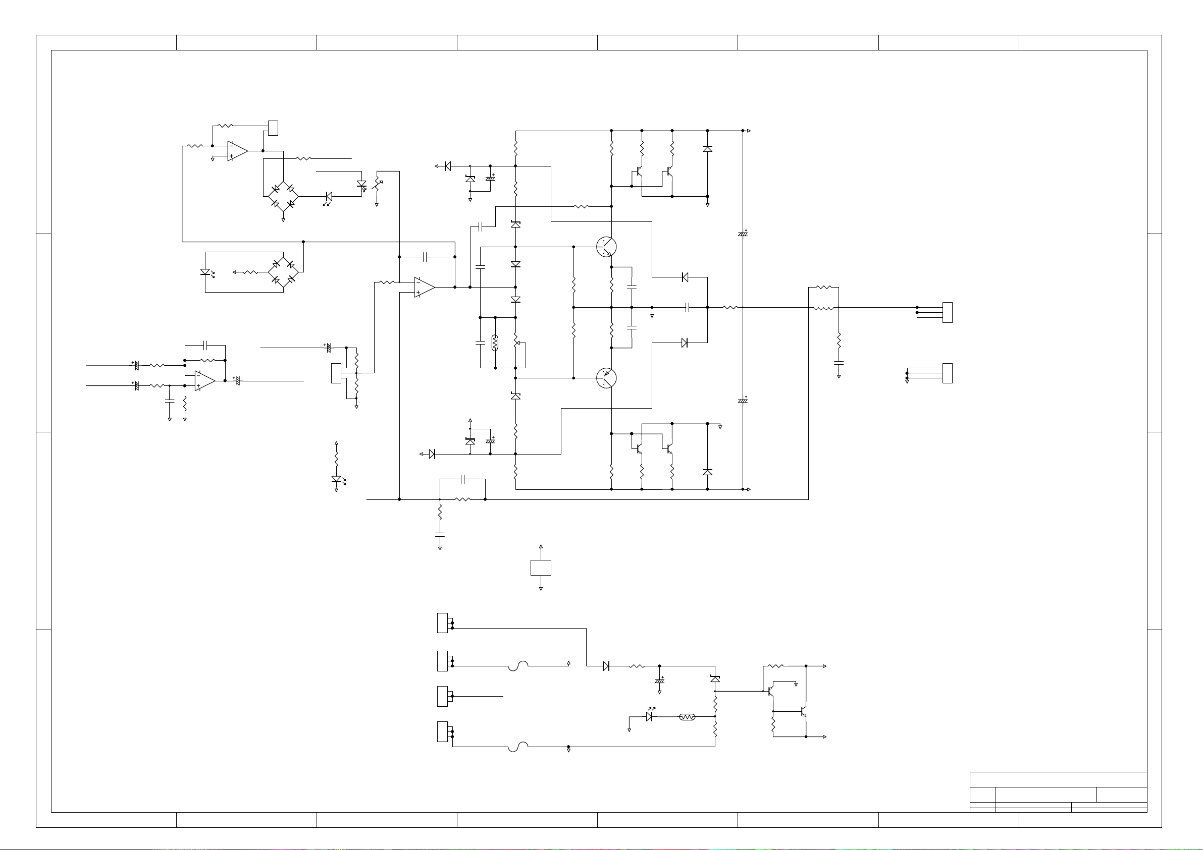
MISTRAL amplifiers include 2 independent channels with separate protection system and
power supply. The independent protection system avoids opening circuit, short, wrong loading or
over-heating. The special-designed protective system applies automatically restarting functions
upon the default status and then goes back to normal.
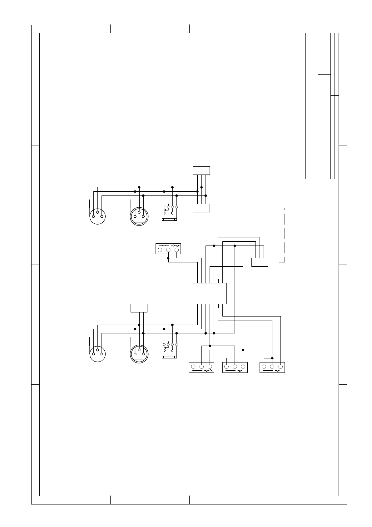
All electronic inputs equip standard power connectors. And all inputs are electronic balanced,
with hi-quality transformer, MISTRAL amplifiers provide an outstanding performance in any
conditions.
zInnovative design and high stability power amplifiers.
zFan-cooled AB class high power amplifier in 19”rack, 2Usize
zRugged amplifiers in a strong, compact chassis.
z2 independent channels with separate protection system and power supply
zsmart-designed protection system for auto re-operation after fault.
zAuto-adjusting speed fan.
z4LEDs for operation/protection, limit, power on and clip
zHIGH-CURRENT TOROIDAL TRANSFORMER DESIGNED FOR HIGH POWER AT 2
Ohms with low noise.
zIndependent DC and thermal overload protection on each channel.
zIEC standard power connectors.
zBinding post and NEUTRIK® SPEAKON outputs power connectors.
zBalanced XLR inputs/ parallel outputs.

3
2. Specification
Output Power DPA 900 DPA 1500
20Hz-20KHz @0.1% THD, SCD MODE
8Ohms per channel(EIAJ) 190W 300W
4Ohms per channel (EIAJ) 300W 500W
Bridge MONO mode
8Ohms ,1KHz, 0.1% THD 600W 1000W
Distortion (SMPTE-IM) <0.05%
Frequency response 20Hz-20KHz=/-0.1dB, -3dB points:10Hz-60Hz
Damping factor ,1 kHz and below >300 at 8 Ohms
Signal to noise ,20Hz`20KHz 102dB
Voltage Gain 40 Χ(32dB)
Input sensitivity @4Ohms 1Vrms
Input clipping 10Vrms(+22dB)
Input impedance 10kOhms unbalanced, 20k Ohms balanced 56(36dB)
Controls Front :AC switch ,CH1&CH2 Gain knobs
Rear :Limiter bridge selector
Indicators (1per channel)
Power-on : Blue LED
Operation/Protection: Dual Color(green/red LED)
Limit: Red LED
Clip: Red LED
Connectors, each channel
Input: Active balanced XLR
Parallel output: XLR
Output: NEUTRIK speaker and binding posts
Cooling Continuously variable-speed fan, rear-to front air flow
Load protection On/off muting, DC-fault load grounding relay, internal
fault fuses.
Power requirements 200-240(100-120)VAC 50-60Hz
Dimensions 19”(48.3cm) rack mounting, 3.5”(8.9cm) tall (2rackspaces)
15.9”(40cm)deep (rack mounting to rear support ears)
weight 12.9kg (Net) 14.8kg (Net)

1 2 3 4 5 6 78
A
B
C
D
8
7654321
D
C
B
A
+1
G
2
C1_16
4700uF/80V
12
R1_13
22R 1W
12
R1_19
0.1R 3W
A2
K
1
D1_6
1N4148
+73V_A
A
2K1
D1_15
1N4004
GND1
2xMJL21193
B
CE
Q1_1
MJE15030
1 2
R1_21
470R 3W
1 2
C1_13
22nF/100V poly
1 2
C1_11
3.3nF/50 cer
1 2
C1_12
3.3nF/50 cer
12
R1_17
4R7 1W
12
R1_18
4R7 1W
GND1
A2
K
1D1_19
1N4148
EC
B
Q1_2
MJE15031
A
2K1
D1_10
1N4148
B
CE
Q1_4
1 2
R1_14
22R 1W
1 2
R1_20
0.1R 3W
GND1
-73V_A
A
2K1
D1_17
1N4004
A2
K
1
D1_11
1N4937
A2
K
1
D1_12
1N4937
1 2
C1_9
2.2nF/50 cer
12
C1_10
22nF/50 cer
A
2K1
D1_13
ZD5V6 1/2W
12
R1_9
820R
12
R1_11
1K5 2W
12
R1_10
820R
1 2
R1_12
1K5 2W
A
2K1
D1_14
ZD5V6 1/2W
A
2K1
D1_7
1N4148
Vic+
A
2K1
D1_3
ZD15V1.3W
+1
G
2
C1_8
220uF/25V
GND1
12
R1_32
100R
GND1
Vic-
1 2
C1_5
56pF/50 cer
1 2
R1_3
10K
1 2
C1_7
27pF/50 cer
1 2
R1_6
12K SPEAKERS BUS
12
R1_5
330R
12
C1_6
47uF/16NP
GND1
12
R1_30
4K7
12
R1_31
4K7
GND1
CH1 GAIN
+
1G2
C1_27
47uF/25V
A
2K1
D1_8
ZD15V1.3W
+1
G
2
C1_4
220uF/25V
GND1
1 2
C1_25
100pF/50 cer
+
1G2
C1_26
47uF/25V
12
C1_3
100pF/50 cer
+
1G2
C1_23
10uF/50V
GND1
+
1G2
C1_24
10uF/50V
1 2
R1_8
NTC 50R
1
1
22
33
R1_16
TRIMMER 100R
3
21
U1_1A
NJM4580L
5
67
U1_1B
NJM4580L
84
U1_1C
NJM4580L
Vic+
Vic-
B
EC
Q1_3
11
22
33
R1_29
3P-2.5
MIS9-CH1.Sch
Titel
Size
File:
Date:
Drawn By:
Sheet
RevisionModel No:
16-Mar-2004
C.C.LIN
ALTO MISTRAL1500-CH1 DRIVE
32of
MISTRAL1500 VER040302
A2
3
21
U2A
NJM4580L
1 2
R1_42
4K7 1/8W
1 2
R1_41
4K7 1/8W
1
2
3
4
D1_9
W2 - 0 4
GND1
1 2
R1_25
47R
44
1
1
2
233
U1_2
VTL5C2
GND1
(FTR VT90N1 VACTEC+)
GND1
CH1 INSERT OUT
CH1 INSERT IN
1
122
3
344
5
566
7
788
9
910 10
11
11 12 12
13
13 14 14
J4
HEADER 7X2
GND1 GND1
1 2
L1_1
2uH 10A
1 2
R1_26
5R6 2W
12
R1_22
10R 3W
12
C1_2
100nF/250V poly
GND1
CH1 OUTPUT
1+
1-
GND1
TO
SPEAKON PCB
12 R1_36
120K
C1_1
47uF/100V
A
2K1
D1_2
1N4004
12 R1_39
PTC 65R
CH1 PHOTO COUPLER
-15V
+15V
GND1
12
R1_37
12K
(1.5A 200V)
(1.5A 200V)
+1
G
2
C1_15
4700uF/80V
12
R1_7
330R
12
R1_4
330R
11A
6A
6A
12 C1_14
3.3nF/100 poly
1 2
R1_15
150R
0.2A
0.2A
84
U2C
NJM4580L
+15V
-15V
12
D1_18
3mm RED LED
CH1_LIM_SW1
CH1_LIM_SW2
12
D1_21
3mm YELLOW LED
1
12
2J1_6
CON2
1 2
R1_27
10K
1 2
R1_1
10K
1 2
R1_2
10K
12
R1_28
10K
CH1 IN+
CH1 IN-
CH1 IN+
CH1 IN-
CH2 IN+
CH2 IN-
CH1 BRIDGE SWITCH CH2 BRIDGE
CH1_LIM_SW1
CH1_LIM_SW2
CH2_LIM_SW1
CH2_LIM_SW2
CH1 BRIDGE SWITCH
Pout=418W RMS @ 4 Ohm
12
D1_16
3mm GREEN LED
Vic-
Vic+
12
R1_33
3K3 1/2W
OPERATING LED
OUTPUT_1 OUTPUT1
1 2
F1_1
5A
1 2
F1_2
5A
OUTPUT_1
12
R1_34
47K
12
R1_38
10K
100R
10K
A
2K1
D1_5
ZD15V1.3W
1 2
D1_4
5mm RED LED
GND1
GND1
+73V_A
-73V_A
1 2
R1_35
100K
1 2
R1_40
6K8
B
CE
Q1_6
MPSA42
B
EC
Q1_5
MPSA92
Vic+
Vic-
GND1
CLIP
1
1
2
2
3
3
J1_4
CN-PCB6.3
1
1
2
2
3
3
J1_5
CN-PCB6.3
1
2
3
4
D1_20
W2 - 0 4
11
22
33
J1_7
CN-PCB6.3
11
22
33
J1_8
CN-PCB6.3
11
22
33
J1_9
CN-PCB6.3
11
22
33
J1_10
CN-PCB6.3
V+
V-
AC1
GND
1
2
J1_11
CON2
1
2
J2_11
CON2
GND1
CH1 IN+
CH2 IN+
for PBM8
4
3. Schematic Diagram

1 2 3 4 5 6 78
A
B
C
D
8
7654321
D
C
B
A
+1
G
2
C1_16
4700uF/80V
12
R1_13
22R 1W
12
R1_19
0.1R 3W
12
R1_23
0.1R 3W
B
EC
Q1_7
A2
K
1
D1_6
1N4148
+73V_A
A
2K1
D1_15
1N4004
GND1
2xMJL21193
B
CE
Q1_1
MJE15030
1 2
R1_21
470R 3W
1 2
C1_13
22nF/100V poly
1 2
C1_11
3.3nF/50 cer
1 2
C1_12
3.3nF/50 cer
12
R1_17
4R7 1W
12
R1_18
4R7 1W
GND1
A2
K
1D1_19
1N4148
EC
B
Q1_2
MJE15031
A
2K1
D1_10
1N4148
B
CE
Q1_4B
CE
Q1_8
1 2
R1_14
22R 1W
1 2
R1_20
0.1R 3W
1 2
R1_24
0.1R 3W
GND1
-73V_A
A
2K1
D1_17
1N4004
A2
K
1
D1_11
1N4937
A2
K
1
D1_12
1N4937
1 2
C1_9
2.2nF/50 cer
12
C1_10
22nF/50 cer
A
2K1
D1_13
ZD5V6 1/2W
12
R1_9
820R
12
R1_11
2K2 2W
12
R1_10
820R
1 2
R1_12
2K2 2W
A
2K1
D1_14
ZD5V6 1/2W
A
2K1
D1_7
1N4148
Vic+
A
2K1
D1_3
ZD15V1.3W
+1
G
2
C1_8
220uF/25V
GND1
12
R1_32
100R
GND1
Vic-
1 2
C1_5
56pF/50 cer
1 2
R1_3
10K
1 2
C1_7
27pF/50 cer
1 2
R1_6
12K SPEAKERS BUS
12
R1_5
330R
12
C1_6
47uF/16NP
GND1
12
R1_30
4K7
12
R1_31
4K7
GND1
CH1 GAIN
+
1G2
C1_27
47uF/25V
A
2K1
D1_8
ZD15V1.3W
+1
G
2
C1_4
220uF/25V
GND1
1 2
C1_25
100pF/50 cer
+
1G2
C1_26
47uF/25V
12
C1_3
100pF/50 cer
+
1G2
C1_23
10uF/50V
GND1
+
1G2
C1_24
10uF/50V
1 2
R1_8
NTC 50R
1
1
22
33
R1_16
TRIMMER 100R
3
21
U1_1A
NJM4580L
5
67
U1_1B
NJM4580L
84
U1_1C
NJM4580L
Vic+
Vic-
B
EC
Q1_3
11
22
33
R1_29
3P-2.5
MIS15-CH1.Sch
Titel
Size
File:
Date:
Drawn By:
Sheet
RevisionModel No:
2-Mar-2004
C.C.LIN
ALTO MISTRAL1500-CH1 DRIVE
32of
MISTRAL1500 VER040302
A2
3
21
U2A
NJM4580L
1 2
R1_42
4K7 1/8W
1 2
R1_41
4K7 1/8W
1
2
3
4
D1_9
W2 - 0 4
GND1
1 2
R1_25
47R
44
1
1
2
233
U1_2
VTL5C2
GND1
(FTR VT90N1 VACTEC+)
GND1
CH1 INSERT OUT
CH1 INSERT IN
1
122
3
344
5
566
7
788
9
910 10
11
11 12 12
13
13 14 14
J4
HEADER 7X2
GND1 GND1
1 2
L1_1
2uH 10A
1 2
R1_26
5R6 2W
12
R1_22
10R 3W
12
C1_2
100nF/250V poly
GND1
CH1 OUTPUT
1+
1-
GND1
TO
SPEAKON PCB
12 R1_36
120K
C1_1
47uF/100V
A
2K1
D1_2
1N4004
12 R1_39
PTC 65R
CH1 PHOTO COUPLER
-15V
+15V
GND1
12
R1_37
12K
(1.5A 200V)
(1.5A 200V)
+1
G
2
C1_15
4700uF/80V
12
R1_7
330R
12
R1_4
330R
11A
6A
6A
12 C1_14
3.3nF/100 poly
1 2
R1_15
150R
0.2A
0.2A
84
U2C
NJM4580L
+15V
-15V
12
D1_18
3mm RED LED
CH1_LIM_SW1
CH1_LIM_SW2
12
D1_21
3mm YELLOW LED
1
12
2J1_6
CON2
1 2
R1_27
10K
1 2
R1_1
10K
1 2
R1_2
10K
12
R1_28
10K
CH1 IN+
CH1 IN-
CH1 IN+
CH1 IN-
CH2 IN+
CH2 IN-
CH1 BRIDGE SWITCH CH2 BRIDGE
CH1_LIM_SW1
CH1_LIM_SW2
CH2_LIM_SW1
CH2_LIM_SW2
CH1 BRIDGE SWITCH
Pout=418W RMS @ 4 Ohm
12
D1_16
3mm GREEN LED
Vic-
Vic+
12
R1_33
3K3 1/2W
OPERATING LED
OUTPUT_1 OUTPUT1
1 2
F1_1
5A
1 2
F1_2
5A
OUTPUT_1
12
R1_34
47K
12
R1_38
10K
100R
10K
A
2K1
D1_5
ZD15V1.3W
1 2
D1_4
5mm RED LED
GND1
GND1
+73V_A
-73V_A
1 2
R1_35
100K
1 2
R1_40
6K8
B
CE
Q1_6
MPSA42
B
EC
Q1_5
MPSA92
Vic+
Vic-
GND1
CLIP
1
1
2
2
3
3
J1_4
CN-PCB6.3
1
1
2
2
3
3
J1_5
CN-PCB6.3
1
2
3
4
D1_20
W2 - 0 4
11
22
33
J1_7
CN-PCB6.3
11
22
33
J1_8
CN-PCB6.3
11
22
33
J1_9
CN-PCB6.3
11
22
33
J1_10
CN-PCB6.3
V+
V-
AC1
GND
5

1 2 3 4 5 6 78
A
B
C
D
8
7654321
D
C
B
A
+1
G
2
C1_16
4700uF/80V
12
R1_13
22R 1W
12
R1_19
0.1R 3W
12
R1_23
0.1R 3W
B
EC
Q1_7
A2
K
1
D1_6
1N4148
+73V_A
A
2K1
D1_15
1N4004
GND1
2xMJL21193
B
CE
Q1_1
MJE15030
1 2
R1_21
470R 3W
1 2
C1_13
22nF/100V poly
1 2
C1_11
3.3nF/50 cer
1 2
C1_12
3.3nF/50 cer
12
R1_17
4R7 1W
12
R1_18
4R7 1W
GND1
A2
K
1D1_19
1N4148
EC
B
Q1_2
MJE15031
A
2K1
D1_10
1N4148
B
CE
Q1_4B
CE
Q1_8
1 2
R1_14
22R 1W
1 2
R1_20
0.1R 3W
1 2
R1_24
0.1R 3W
GND1
-73V_A
A
2K1
D1_17
1N4004
A2
K
1
D1_11
1N4937
A2
K
1
D1_12
1N4937
1 2
C1_9
2.2nF/50 cer
12
C1_10
22nF/50 cer
A
2K1
D1_13
ZD5V6 1/2W
12
R1_9
820R
12
R1_11
2K2 2W
12
R1_10
820R
1 2
R1_12
2K2 2W
A
2K1
D1_14
ZD5V6 1/2W
A
2K1
D1_7
1N4148
Vic+
A
2K1
D1_3
ZD15V1.3W
+1
G
2
C1_8
220uF/25V
GND1
12
R1_32
100R
GND1
Vic-
1 2
C1_5
56pF/50 cer
1 2
R1_3
10K
1 2
C1_7
27pF/50 cer
1 2
R1_6
12K SPEAKERS BUS
12
R1_5
330R
12
C1_6
47uF/16NP
GND1
12
R1_30
4K7
12
R1_31
4K7
GND1
CH1 GAIN
+
1G2
C1_27
47uF/25V
A
2K1
D1_8
ZD15V1.3W
+1
G
2
C1_4
220uF/25V
GND1
1 2
C1_25
100pF/50 cer
+
1G2
C1_26
47uF/25V
12
C1_3
100pF/50 cer
+
1G2
C1_23
10uF/50V
GND1
+
1G2
C1_24
10uF/50V
1 2
R1_8
NTC 50R
1
1
22
33
R1_16
TRIMMER 100R
3
21
U1_1A
NJM4580L
5
67
U1_1B
NJM4580L
84
U1_1C
NJM4580L
Vic+
Vic-
B
EC
Q1_3
11
22
33
R1_29
3P-2.5
MIS15-CH1.Sch
Titel
Size
File:
Date:
Drawn By:
Sheet
RevisionModel No:
2-Mar-2004
C.C.LIN
ALTO MISTRAL1500-CH1 DRIVE
32of
MISTRAL1500 VER040302
A2
3
21
U2A
NJM4580L
1 2
R1_42
4K7 1/8W
1 2
R1_41
4K7 1/8W
1
2
3
4
D1_9
W2 - 0 4
GND1
1 2
R1_25
47R
44
1
1
2
233
U1_2
VTL5C2
GND1
(FTR VT90N1 VACTEC+)
GND1
CH1 INSERT OUT
CH1 INSERT IN
1
122
3
344
5
566
7
788
9
910 10
11
11 12 12
13
13 14 14
J4
HEADER 7X2
GND1 GND1
1 2
L1_1
2uH 10A
1 2
R1_26
5R6 2W
12
R1_22
10R 3W
12
C1_2
100nF/250V poly
GND1
CH1 OUTPUT
1+
1-
GND1
TO
SPEAKON PCB
12 R1_36
120K
C1_1
47uF/100V
A
2K1
D1_2
1N4004
12 R1_39
PTC 65R
CH1 PHOTO COUPLER
-15V
+15V
GND1
12
R1_37
12K
(1.5A 200V)
(1.5A 200V)
+1
G
2
C1_15
4700uF/80V
12
R1_7
330R
12
R1_4
330R
11A
6A
6A
12 C1_14
3.3nF/100 poly
1 2
R1_15
150R
0.2A
0.2A
84
U2C
NJM4580L
+15V
-15V
12
D1_18
3mm RED LED
CH1_LIM_SW1
CH1_LIM_SW2
12
D1_21
3mm YELLOW LED
1
12
2J1_6
CON2
1 2
R1_27
10K
1 2
R1_1
10K
1 2
R1_2
10K
12
R1_28
10K
CH1 IN+
CH1 IN-
CH1 IN+
CH1 IN-
CH2 IN+
CH2 IN-
CH1 BRIDGE SWITCH CH2 BRIDGE
CH1_LIM_SW1
CH1_LIM_SW2
CH2_LIM_SW1
CH2_LIM_SW2
CH1 BRIDGE SWITCH
Pout=418W RMS @ 4 Ohm
12
D1_16
3mm GREEN LED
Vic-
Vic+
12
R1_33
3K3 1/2W
OPERATING LED
OUTPUT_1 OUTPUT1
1 2
F1_1
5A
1 2
F1_2
5A
OUTPUT_1
12
R1_34
47K
12
R1_38
10K
100R
10K
A
2K1
D1_5
ZD15V1.3W
1 2
D1_4
5mm RED LED
GND1
GND1
+73V_A
-73V_A
1 2
R1_35
100K
1 2
R1_40
6K8
B
CE
Q1_6
MPSA42
B
EC
Q1_5
MPSA92
Vic+
Vic-
GND1
CLIP
1
1
2
2
3
3
J1_4
CN-PCB6.3
1
1
2
2
3
3
J1_5
CN-PCB6.3
1
2
3
4
D1_20
W2 - 0 4
11
22
33
J1_7
CN-PCB6.3
11
22
33
J1_8
CN-PCB6.3
11
22
33
J1_9
CN-PCB6.3
11
22
33
J1_10
CN-PCB6.3
V+
V-
AC1
GND
6

1 2 3 4 5 6 78
A
B
C
D
8
7654321
D
C
B
A
+1
G
2
C2_16
4700uF/80V
12
R2_13
22R 1W
12
R2_19
0.1R 3W
12
R2_23
0.1R 3W
B
EC
Q2_7
A2
K
1
D2_6
1N4148
+73V_B
A
2K1
D2_15
1N4004
GND1
2xMJL21193
B
CE
Q2_1
MJE15030
1 2
R2_21
470R 3W
1 2
C2_13
22nF/100V poly
1 2
C2_11
3.3nF/50 cer
1 2
C2_12
3.3nF/50 cer
12
R2_17
4R7 1W
12
R2_18
4R7 1W
GND1
A2
K
1D2_19
1N4148
EC
B
Q2_2
MJE15031
A
2K1
D2_10
1N4148
B
CE
Q2_4B
CE
Q2_8
1 2
R2_14
22R 1W
1 2
R2_20
0.1R 3W
1 2
R2_24
0.1R 3W
GND1
-73V_B
A
2K1
D2_17
1N4004
A2
K
1
D2_11
1N4937
A2
K
1
D2_12
1N4937
1 2
C2_9
2.2nF/50 cer
12
C2_10
22nF/50 cer
A
2K1
D2_13
ZD5V6 1/2W
12
R2_9
820R
12
R2_11
2K2 2W
12
R2_10
820R
1 2
R2_12
2K2 2W
A
2K1
D2_14
ZD5V6 1/2W
A
2K1
D2_7
1N4148
Vic2+
A
2K1
D2_3
ZD15V1.3W
+1
G
2
C2_8
220uF/25V
GND1
1
2
3
4
D2_20
W2 - 0 4
12
R2_32
100R
GND1
Vic2-
1 2
C2_5
56pF/50 cer
1 2
R2_3
10K
1 2
C2_7
27pF/50 cer
1 2
R2_6
12K SPEAKERS BUS
12
R2_5
330R
12
C2_6
47uF/16NP
GND1
12
R2_30
4K7
12
R2_31
4K7
GND1
CH1 GAIN
+
1G2
C2_27
47uF/25V
A
2K1
D2_8
ZD15V1.3W
+1
G
2
C2_4
220uF/25V
GND1
1 2
C2_25
100pF/50 cer
+
1G2
C2_26
47uF/25V
12
C2_3
100pF/50 cer
+
1G2
C2_23
10uF/50V
GND1
+
1G2
C2_24
10uF/50V
1 2
R2_8
NTC 50R
1
1
22
33
R2_16
TRIMMER 100R
3
21
U2_1A
NJM4580L
5
67
U2_1B
NJM4580L
B
EC
Q2_3
11
22
33
R2_29
3P-2.5
MIS15-CH2.Sch
Titel
Size
File:
Date:
Drawn By:
Sheet
RevisionModel No:
2-Mar-2004
C.C.LIN
ALTO MISTRAL1500-CH1 DRIVE
33of
MISTRAL1500 VER040302
A2
5
67
U2B
NJM4580L
1 2
R2_42
4K7 1/8W
1 2
R2_41
4K7 1/8W
1
2
3
4
D2_9
W2 - 0 4
GND1
1 2
R2_25
47R
44
1
1
2
233
U2_2
VTL5C2
GND1
(FTR VT90N1 VACTEC+)
GND1
CH2 INSERT OUT
CH2 INSERT IN
12 L2_1
2uH 10A
1 2
R2_26
5R6 2W
12
R2_22
10R 3W
12
C2_2
100nF/250V poly
GND1
CH1 OUTPUT
1+
1-
GND1
TO
SPEAKON PCB
12 R2_36
120K
+1
G
2
C2_1
47uF/100V
A
2K1
D2_2
1N4004
12 R2_39
PTC 65R
CH1 PHOTO COUPLER
-15V
+15V
GND1 (1.5A 200V)
(1.5A 200V)
+1
G
2
C2_15
4700uF/80V
12
R2_7
330R
12
R2_4
330R
11A
6A
6A
12 C2_14
3.3nF/100 poly
1 2
R2_15
150R
0.2A
0.2A
12
D2_18
3mm RED LED
CH2_LIM_SW1
CH2_LIM_SW2
12
D2_21
3mm YELLOW LED
1
12
2J2_6
CON2
1 2
R2_27
10K
1 2
R2_1
10K
1 2
R2_2
10K
12
R2_28
10K
CH2 IN+
CH2 IN-
CH2 BRIDGE
Pout=418W RMS @ 4 Ohm
12
D2_16
3mm GREEN LED
Vic2-
Vic2+
12
R2_33
3K3 1/2W
OPERATING LED
OUTPUT_2 OUTPUT2
1 2
F2_1
5A
1 2
F2_2
5A
OUTPUT_2
12
R2_34
47K
12
R2_38
10K
100R
10K
A
2K1
D2_5
ZD15V1.3W
1 2
D2_4
5mm RED LED
GND1
GND1
+73V_B
-73V_B
1 2
R2_35
100K
1 2
R2_40
6K8
B
CE
Q2_6
MPSA42
B
EC
Q2_5
MPSA92
Vic2+
Vic2-
GND1
CLIP
84
U2_1C
NJM4580L
Vic2+
Vic2-
1
1
2
2
3
3
J2_4
CN-PCB6.3
1
1
2
2
3
3
J2_5
CN-PCB6.3
11
22
33
J2_7
CN-PCB6.3
11
22
33
J2_8
CN-PCB6.3
11
22
33
J2_9
CN-PCB6.3
11
22
33
J2_10
CN-PCB6.3
V+
V-
AC1
GND
7

1 2 34
A
B
C
D
4
321
D
C
B
A
12
34
56
78
910
11 12
13 14
CN1
HEADER 7X2
2
1
3
4
CN3
CH1-XLR-IN
2
1
3
4
CN2
CH1-LINK-OUT
1
2
3
SW1A
BRIDGE
4
5
6
P
SW1B
BRIDGE
1
2
3
SW2A
LIMITER
4
5
6
P
SW2B
LIMITER
2
1
3
4
PJ1
CH1-JACK-IN
2
1
3
4
CN5
CH2-XLR-IN
2
1
3
4
CN4
CH2-LINK-OUT
2
1
3
4
PJ2
CH2-JACK-IN
1
2
3
CN7
CON3
1
2
3
CN6
CON3
1
2
3
CN8
CON3
1
2
3
CN9
CON3
MIS15IN.Sch
Titel
Size
File:
Date:
Drawn By:
Sheet
RevisionModel No:
8-Mar-2004
C.C.LIN
ALTO : MISTRAL1500
11of
MISTRAL1500 VER040204
A3
8

1 2 34
A
B
C
D
4
321
D
C
B
A
1
2
D2_30
3mm YELLOW LED
1
2
D2_3
3mm RED LED
1
2
D2_29
3mm BLUE LED
LIMITER
CLIP
ON/PROTECTION
1
2
D2_1
3mm GREEN LED
POWER ON
1
2
D1_30
3mm YELLOW LED
1
2
D1_3
3mm RED LED
1
2
D1_29
3mm BLUE LED
LIMITER
CLIP
ON/PROTECTION
1
2
D1_1
3mm GREEN LED
POWER ON
VR1_1
B50K
VR2_1
B50K
1
2
3
CN1_1
3P2.5
1
2
3
CN2_1
3P2.5
1
2
3
4
5
6
7
8
9
10
11
12
13
14
CN3
CON14
MIS15FP.Sch
Titel
Size
File:
Date:
Drawn By:
Sheet
RevisionModel No:
8-Mar-2004
C.C.LIN
ALTO : MISTRAL1500
11of
MISTRAL1500 VER040204
A3
9

1 2 34
A
B
C
D
4
321
D
C
B
A
11
22
33
J2
HEADER 3
+1
G
2
C1
470uF/35V
IN
IN
G
G
OUT OUT
U1
LM317T
12 R1
3K3
1 2
R2
47R
12
C2
100nF/50 cer
+1
G
2
C3
10uF/63
+24V
FAN
1 2
R3
NTC 100R
(1.5A 200V)
12V
12V
+1
G
2
C4
470uF/35V
+1
G
2
C5
470uF/35V
12 R5
0R
12
R4
3K3
1 2
D2
3mm GREEN LED
POWER ON LED
+1
G
2
C6
10uF/50 1
1
2
2
3
3
J3
CON3
1
122
3
344
5
566
7
788
9
910 10
J1
HEADER 5X2
CH1 INSERT OUTCH1 INSERT IN
CH2 INSERT OUTCH2 INSERT IN
GND1 GND1
+15V-15V
GNDF GNDF GND1
MIS15
MIS15-CH1.SCH
MIS15
MIS15-CH2.SCH
MIS15-FAN.Sch
Titel
Size
File:
Date:
Drawn By:
Sheet
RevisionModel No:
2-Mar-2004
C.C.LIN
ALTO MISTRAL1500 FAN
31of
MISTRAL1500 VER040302
A4
+15V
-15V
1
2
3
4
D1
W2-04
10

11

12

4.PCB Layout
MIS15FP
Top overlay
Bottom layer
13

MIS151N1
Top overlay
Bottom layer
MIS151N2
Top overlay
Bottom layer
14

Top layer
15
MIS15MN

Top overlay
16

Bottom layer
17

5. Test Procedure & Test Result
DPA900/1500 TEST PROCEDURE
DSP Test
Instruments
1. DMM
2. Audio Analyze unit (VP-7724)
3. Oscillograph
4. PC with RS232 port
Test Procedure
Step1: Visual check
Visually check if the cosmetic of the amplifier and assembly are OK.
Step2: Set up
zTurn off power
zSet the output sine wave signal of the VP-7724 is 0.775V(0dB)/1KHz, then connect output
of VP-7724 with input of CH1 of amplifier.
zConnect the DMM with output of CH1 of amplifier
zConnect the CH1 of oscillograph with CH1 of amplifier, connect the CH2 of oscillograph
with CH2 of amplifier
zConnect the 4 Ohm load with CH1 and CH2 of amplifier respectively.
zTurn the volume knob counter clockwise fully.
Step 3: Power supply test
zPlug the amplifier into mains, turn on the amplifier
zMake sure all the voltage values are correct, then turn off power.
Step 4: DSP Test
4.1 press the “ENTER” and “SEL” at the same time. The unit will enter the test modal and
check as following:
a. All LEDs will light up in sequence.
b. The display will show “8.8” .
4.2 Press the “ENTER” and “SEL” at the same time.
a. Press “UP”, the display will show “1”.
b. Press “DOWN”, the display will show “2”.
c. Press “ENTER”, the display will show “3”.
d. Press “SEL”, the display will show “4”.
Step5: Test EEPROM
1. Press “ENTER” and “SEL” again, the LED (HUM CANCEL) should be light up. After wait
about 50 seconds, check as following:
a. If the display show “01” , the test is ok
b. If the display show “E1”, the test fails.
18

Step6: Test RAM
1. Press “ENTER” and “SEL” at the same time again, the LED(NOISE GATE) will light up,
wait a few seconds, check as following:
a. If the display show “02”, the test is ok.
b. If the display show “E2”, the test fails .
Step7. RS232 Port Test
1. Turn off the unit, then connect the computer and the amplifier via RS232 port, then turn on
the unit.
2. If the panel shows”56”, the Connection is ok.
3. Done.
PCB Test
Instruments
1. DMM
2. Audio Analyzer unit
3. Oscillograph
4. 8Ω(400W) load
1) Test procedures and specification
1.Set LIMITER and BRIDGE switches in the position OFF. Turn VR of CH1 and CH2 to
maximum, then turn on the power switch and the blue power LED lights up, and
OPERATING/PROTECTION LED shows red, then it turns green after 2-5 seconds or so.
2. Without signal input, adjust R1-16(CH1) and R2-16(CH2) so that the voltage of R1-17/2-17 is
125±2Mv(DPA900)/130±2mV. Connect a 4Ωload at output. Input a 5KHz signal into CH1 or
CH2. Adjust the signal so that the output is 5VP-P (about 2VRMS). Verify the curve on
oscilloscope and there should be no crossover distortion.
3. Input a 1KHz,-6dB signal. The output should be 26V+/-0.5V( for DPA900) and 37V+/-
0.5V(for DPA1500), and the distortion should be less than 1%. Using the multifunctional meter
to measure two pins of JP3, the voltage is about 12V at first, then use a heat blower to blow R3.
The voltage will increase up to about 26V. Using a tweezers to short-circuit R1-38 (CH1) and
R2-38(CH2). The overheat protection will start (no signal output).
4. Short-circuit the output terminal while it reaches maximum output level. The LIMITER on
19
This manual suits for next models
1
Table of contents
Other Alto Amplifier manuals

Alto
Alto DPA 2500 User manual

Alto
Alto MC250.8 User manual

Alto
Alto MISTRAL 1500 User manual

Alto
Alto MP2D User manual

Alto
Alto STEREO TUBE PREAMP User manual

Alto
Alto MAC 2.2, MAC 2.3, MAC 2.4 User manual

Alto
Alto MISTRAL2500 User manual

Alto
Alto ? MICtube User manual

Alto
Alto APX2000 User manual

Alto
Alto A400.4 Dragonfly User manual