Analog Devices MAX98388 User manual

Click here to ask an associate for production status of specific part numbers.
Digital Input Class-D Amplifier with
IV Feedback and Brownout Protection
MAX98388/MAX98389
19-101683; Rev 0; 3/23
© 2023 Analog Devices, Inc. All rights reserved. Trademarks and registered trademarks are the property of their respective owners.
General Description
The MAX98388/MAX98389 is a small, cost-effective
mono digital input amplifier with integrated IV feedback.
The device operates over a wide supply voltage range
from 2.3V to 10V. With this supply range, both versions
support single-cell, two-cell, and externally
regulated/boosted portable applications. MAX98388 is
optimized for up to 5.5V applications (single-cell), while
MAX98389 is optimized for 5V to 10V cases (two-cell).
The Class-D playback amplifier pairs Class-AB level
audio performance with the efficiency needed to extend
battery life in portable applications. Active emissions-
limiting (AEL) and edge-rate limiting circuitry combined
with a spread-spectrum modulation (SSM) scheme
reduces EMI and eliminates the need for the output
filtering required for traditional Class-D amplifiers.
The device provides a precision output current sense
channel and an output voltage feedback channel. The
data collected by these channels can be transmitted on
the audio data output and enables algorithms such as
audio enhancement, bass boosting, speaker protection,
and haptic functions to be run on the host audio DSP.
The device includes a programmable threshold playback
channel ALC that provides brownout protection for
batteries in portable systems, and robust thermal and
overcurrent protection to prevent device damage.
The device provides a PCM interface for audio playback
and IV feedback data and pairs this with a standard I2C
interface for device control and status readback. The
PCM interface supports common audio data formats
such as I2S, left justified, and TDM timing. A unique
clocking structure eliminates the need for an external
high-frequency reference clock. In addition to reducing
device size and pin count, eliminating this clock saves
interface power while reducing the risk of EMI from high-
speed switching and potential board coupling issues.
The package connections are designed to only require
edge routing, allowing the use of the cost-effective
wafer-level package (WLP) with no requirement for
expensive bump vias. The device is available in a 0.4mm
pitch 16-bump WLP package and is specified over the
extended -40°C to +85°C temperature range.
SMBus is a trademark of Intel Corp.
Benefits and Features
•Wide Amplifier Supply Range (2.3V to 10V)
•Supports Both Single-Cell and Two-Cell Cases
•High-Performance Class-D Amplifier
•Up to 111dB Dynamic Range (A-Weighted)
•10μVRMS Output Noise (Single-Cell Mode)
•14.5μVRMS Output Noise (Two-Cell Mode)
•High Output Power (THD+N ≤ 1%)
•1.32W Output Power into 4Ω (VPVDD = 3.7V)
•2.4W Output Power into 4Ω (VPVDD = 5V)
•5.15W Output Power into 4Ω (VPVDD = 7.4V)
•9.1W Output Power into 4Ω (VPVDD = 10V)
•High Amplifier Efficiency (Playback Only Power)
•76% Efficiency at 0.1W into 4Ω (VPVDD = 5V)
•85.5% Efficiency at 1W into 4Ω (VPVDD = 5V)
•90% Efficiency at 1W into 8Ω (VPVDD = 5V)
•Peak THD+N Better than -83dB at 1kHz
•Low Total Quiescent Power
•9.3mW (VPVDD = 3.7V, IV Feedback Disabled)
•13.9mW (VPVDD = 3.7V, IV Feedback Enabled)
•16.1mW (VPVDD = 5V, IV Feedback Enabled)
•22.5mW (VPVDD = 7.4V, IV Feedback Enabled)
•Low < 5µW Software Shutdown Power
•1ms Turn-On Time (fS= 48kHz, Ramp Disabled)
•Five Sample Playback Delay (fS< 50kHz, fIN = 1kHz)
•No External Reference Clock Required
•Playback Sample Rates from 8kHz to 96kHz
•Trimmed Class-D Switching Frequency for EMI Planning
•Extensive Click-and-Pop Reduction Circuitry
•Programmable ALC for Brownout Protection
•Robust Short-Circuit and Thermal Protection
•Available in Space-Saving Package:
•2.93mm2, 16-pin WLP (0.4mm Pitch)
Applications
•AR/VR Wearables
•LRA Haptic Drive
•Smart Watches and IoT Devices
•Gaming Devices
•Notebooks and Tablets
Ordering Information appears at end of data sheet.
MAX98388/MAX98389
Digital Input Class-D Amplifier with
IV Feedback and Brownout Protection
www.analog.com
Analog Devices | 2
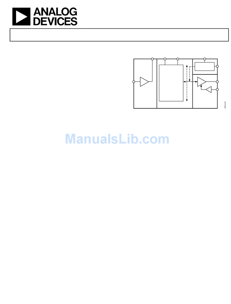
Simplified Block Diagram
MAX98388
MAX98389
PCM
(I2S/TDM)
BUS
I2C CONTROL
BUS
VOLTAGE
FEEDBACK
CHANNEL
ISENSE
FEEDB ACK
CHANNEL
PCM AUDIO
INTERFACE
PLAY BACK
CHANNEL DAC
ISENSE
ADC
BROWNOUT
PROTECTION
CLASS-D
ADDRESS
SELECT
I2C SLAVE
INTERFACE
POWER/STATE
MANAGEM ENT
SPEAKER
OUTPUT
VDD (1.8V) HARDWARE
RESET
PVDD
(2.3V TO 10V)
THERMAL
PROTECTION

MAX98388/MAX98389
Digital Input Class-D Amplifier with
IV Feedback and Brownout Protection
www.analog.com
Analog Devices | 3
Absolute Maximum Ratings
GND to PGND ...................................................-0.1V to +0.1V
VPVDD to PGND...................................................-0.3V to +12V
VDD to GND........................................................-0.3V to +2.2V
OUTP, OUTN to PGND ........................-0.3V to VPVDD + 0.3V
BCLK, LRCLK, DIN, DOUT to GND..........-0.3V to VDD + 0.3V
ADDR, I.C. to GND................................... -0.3V to VDD + 0.3V
All Other Pins to GND........................................-0.3V to +2.2V
Duration of short between OUTP and OUTN..........Continuous
Duration of short circuit between OUTP or OUTN and PGND,
PVDD, or VDD........................................................ Continuous
Continuous power dissipation (TA= +70°C, derate 13.7mW/°C
above +70°C).................................................................1.38W
Junction temperature ................................................... +150°C
Operating temperature range........................... -40°C to +85°C
Storage temperature range............................ -65°C to +150°C
Soldering temperature (reflow)..................................... +260°C
Stresses beyond those listed under “Absolute Maximum Ratings” may cause permanent damage to the device. These are stress ratings only, and functional operation of the device at these or
any other conditions beyond those indicated in the operational sections of the specifications is not implied. Exposure to absolute maximum rating conditions for extended periods may affect
device reliability.
Package Information
WLP
Package Code
W161P1Z+1
Outline Number
21-100636
Land Pattern Number
Refer to Application Note 1891
Thermal Resistance, Four Layer Board:
Junction-to-Ambient (θJA)
57.93°C/W
Junction-to-Case Thermal Resistance (θJC)
N/A
For the latest package outline information and land patterns (footprints), go to www.maximintegrated.com/packages. Note that a “+”,
“#”, or “-” in the package code indicates RoHS status only. Package drawings may show a different suffix character, but the drawing
pertains to the package regardless of RoHS status.
Package thermal resistances were obtained using the method described in JEDEC specification JESD51-7, using a four-layer board.
For detailed information on package thermal considerations, refer to www.maximintegrated.com/thermal-tutorial.

MAX98388/MAX98389
Digital Input Class-D Amplifier with
IV Feedback and Brownout Protection
www.analog.com
Analog Devices | 4
Electrical Characteristics
(VPVDD = 5V (Single-Cell Mode) or 7.4V (Two-Cell Mode), VDD = 1.8V, VGND = VPGND = 0V, CPVDD = 10μF + 0.1μF, CVDD = 1μF,
fBCLK = 3.072MHz, fLRCLK = 48kHz, ZSPK = ∞ between OUTP and OUTN, Single-Cell Mode, AC Measurement Bandwidth = 20Hz to
20kHz, TA= TMIN to TMAX, Typical values are at TA= +25°C) (Note 1)
PARAMETER
SYMBOL
CONDITIONS
MIN
TYP
MAX
UNITS
SYSTEM-LEVEL
PVDD Supply Voltage
Range
VPVDD
Guaranteed by
PSRR test
Two-cell/
boosted mode
5
10
V
Single-cell mode
3.0
5.5
Guaranteed by PSRR test, single-cell
mode, the device is functional but
parametric performance is not
guaranteed
2.3
VDD Supply Voltage
Range
VDD
Guaranteed by PSRR test
1.71
1.8
1.89
V
PVDD Undervoltage
Lockout
VUVLO_PVDD
Single-cell mode
VPVDD falling
1.9
2.2
V
Two-cell mode
VPVDD falling
4.4
4.7
PVDD UVLO Hysteresis
Single-cell mode (Note 4)
150
200
mV
Two-cell mode (Note 4)
120
150
VDD Undervoltage
Lockout
VUVLO_VDD
VDD falling
1.3
1.6
V
VDD UVLO Hysteresis
Note 4
20
40
mV
VDD Supply Ramp Rate
0.1
V/ms
Thermal Shutdown
Temperature
THERMSHDN_THRES = 0x2
155
°C
Thermal Shutdown
Hysteresis
15
°C
Thermal Warning
Temperature
THERMWARN_THRES = 0x2
115
°C
Thermal Warning
Hysteresis
15
°C
POWER CONSUMPTION / QUIESCENT POWER CONSUMPTION
Total Quiescent Power
Both supplies, IV
feedback disabled
VPVDD = 3.7V
9.3
mW
Both supplies, IV
feedback enabled
VPVDD = 3.7V
13.9
VPVDD = 5V
16.1
VPVDD = 7.4V
22.5
PVDD Quiescent
Current
IV feedback
disabled
VPVDD = 3.7V
1.37
mA
VDD Quiescent Current
IV feedback disabled
2.38
mA
PVDD Quiescent
Current
IV feedback
enabled
VPVDD = 3.7V
1.42
2
mA
VPVDD = 5V
1.59
2.2
VPVDD = 7.4V
1.86
2.5
VDD Quiescent Current
IV feedback enabled
4.83
6.8
mA
POWER CONSUMPTION / SOFTWARE SHUTDOWN POWER CONSUMPTION
PVDD Software
Shutdown Current
IPVDD_SWSD
No toggling on
PCM interface pins,
TA= +25°C
VPVDD = 3.7V,
single-cell mode
0.3
4
µA
VPVDD = 7.4V,
two-cell mode
0.4
5

MAX98388/MAX98389
Digital Input Class-D Amplifier with
IV Feedback and Brownout Protection
www.analog.com
Analog Devices | 5
(VPVDD = 5V (Single-Cell Mode) or 7.4V (Two-Cell Mode), VDD = 1.8V, VGND = VPGND = 0V, CPVDD = 10μF + 0.1μF, CVDD = 1μF,
fBCLK = 3.072MHz, fLRCLK = 48kHz, ZSPK = ∞ between OUTP and OUTN, Single-Cell Mode, AC Measurement Bandwidth = 20Hz to
20kHz, TA= TMIN to TMAX, Typical values are at TA= +25°C) (Note 1)
PARAMETER
SYMBOL
CONDITIONS
MIN
TYP
MAX
UNITS
VDD Software Shutdown
Current
IVDD_SWSD
No toggling on PCM interface pins, TA=
+25°C
1.5
6
µA
POWER CONSUMPTION / HARDWARE SHUTDOWN POWER CONSUMPTION
PVDD Hardware
Shutdown Current
IPVDD_HWSD
TA= +25°C
VPVDD = 3.7V,
single-cell mode
0.3
4
µA
VPVDD = 7.4V,
two-cell mode
0.4
5
VDD Hardware
Shutdown Current
IVDD_HWSD
TA= +25°C
0.2
1
µA
ENABLE / DISABLE TIMING
Turn-On Time
tON
Software-shutdown
state to active state
(device ready to
receive audio data)
Volume ramp
disabled, fS≥
44.1kHz
0.6
1
ms
Volume ramp
disabled, fS<
44.1kHz (Note 4)
1.1
2.3
Volume ramp
enabled, fS≥
44.1kHz
2.3
2.7
Volume ramp
enabled, fS<
44.1kHz (Note 4)
2.9
4.2
Turn-Off Time
tOFF
From full-active
state operation to
software-shutdown
state (power down
done status)
Volume ramp
disabled
70
100
µs
Volume ramp
enabled,
fS≥ 44.1kHz
4.3
4.6
ms
Volume ramp
enabled,
fS< 44.1kHz
6.7
8
Hardware Enable Time
tHW_EN
Transition time from the hardware-
shutdown state (RESET input set high) to
the software-shutdown state (I2C ready)
1.5
ms
Hardware Reset Time
tHW_RES
Transition time from software reset (write
1 to the software reset bit) until the device
is reset and returns to the software-
shutdown state (I2C ready)
0.4
ms
Hardware Disable
Assert Time
tHW_DIS
Minimum time RESET input must be
asserted low to ensure the device
transitions to the hardware-shutdown
state
1
µs
SPEAKER DIGITAL AUDIO CHANNEL / DAC DIGITAL FILTER CHARACTERISTICS (fLRCLK < 50kHz) (Note 2)
Passband Cutoff
Frequency
fPLP
Ripple < δP
0.452 x
fS
Hz
Droop < -3dB
0.457 x
fS
Passband Ripple
δP
fIN < fPLP, referenced to signal level at
1kHz, digital filter response only
-0.1
+0.1
dB
Stopband Cutoff
Frequency
fSLP
Attenuation > δS
0.49 x
fS
Hz

MAX98388/MAX98389
Digital Input Class-D Amplifier with
IV Feedback and Brownout Protection
www.analog.com
Analog Devices | 6
(VPVDD = 5V (Single-Cell Mode) or 7.4V (Two-Cell Mode), VDD = 1.8V, VGND = VPGND = 0V, CPVDD = 10μF + 0.1μF, CVDD = 1μF,
fBCLK = 3.072MHz, fLRCLK = 48kHz, ZSPK = ∞ between OUTP and OUTN, Single-Cell Mode, AC Measurement Bandwidth = 20Hz to
20kHz, TA= TMIN to TMAX, Typical values are at TA= +25°C) (Note 1)
PARAMETER
SYMBOL
CONDITIONS
MIN
TYP
MAX
UNITS
Stopband Attenuation
δS
fIN > fSLP
75
dB
Group Delay
fIN = 1kHz
5
samples
SPEAKER DIGITAL AUDIO CHANNEL / DAC DIGITAL FILTER CHARACTERISTICS (fLRCLK
Passband Cutoff
Frequency
fPLP
Ripple < δP
0.227 x
fS
Hz
Droop < -3dB
0.314 x
fS
Passband Ripple
δP
fIN < fPLP, referenced to signal level at
1kHz, digital filter response only
-0.1
+0.1
dB
Stopband Cutoff
Frequency
fSLP
Attenuation < δS
0.49 x
fS
Hz
Stopband Attenuation
δS
fIN > fSLP
80
dB
Group Delay
fIN = 1kHz
5.5
samples
SPEAKER DIGITAL AUDIO CHANNEL / DC BLOCKING DIGITAL FILTER CHARACTERISTICS (Note 2)
DC Attenuation
80
dB
DC Blocking Filter -3dB
Cutoff Frequency
fC
fS= 8kHz, 16kHz, 32kHz, 48kHz, and
96kHz
1.872
Hz
fS= 44.1kHz, 88.2kHz
1.72
SPEAKER CLASS-D AMPLIFIER
Output Offset Voltage
VOS
TA= +25°C
-3
±0.3
+3
mV
Click-and-Pop Level
KCP
Peak voltage, A-
weighted, 32
samples per
second, digital
silence used for
input signal, ZSPK
= 8Ω + 33μH or 4Ω
+ 33μH
Amp output power
down, single-cell
mode
-77
dBV
Amp output power
down, two-cell
mode
-71
Amp output power-
up, single-cell
mode
-76
Amp output power-
up, two-cell mode
-70
Output Noise
eN
A-weighted, 24-bit,
or 32-bit data
Single-cell mode,
DAC low-power
mode
10
µVRMS
Two-cell mode,
DAC high-
performance mode
14.5
Dynamic Range
DR
A-weighted, 24-bit
or 32-bit data,
single-cell mode,
DAC low power
mode (Note 3)
ZSPK = 4Ω + 33µH
110
dB
ZSPK = 8Ω + 33µH
110.5
A-weighted, 24-bit
or 32-bit data, two-
cell mode, VPVDD
= 7.4V, DAC high-
performance mode
(Note 3)
ZSPK = 8Ω + 33µH
111

MAX98388/MAX98389
Digital Input Class-D Amplifier with
IV Feedback and Brownout Protection
www.analog.com
Analog Devices | 7
(VPVDD = 5V (Single-Cell Mode) or 7.4V (Two-Cell Mode), VDD = 1.8V, VGND = VPGND = 0V, CPVDD = 10μF + 0.1μF, CVDD = 1μF,
fBCLK = 3.072MHz, fLRCLK = 48kHz, ZSPK = ∞ between OUTP and OUTN, Single-Cell Mode, AC Measurement Bandwidth = 20Hz to
20kHz, TA= TMIN to TMAX, Typical values are at TA= +25°C) (Note 1)
PARAMETER
SYMBOL
CONDITIONS
MIN
TYP
MAX
UNITS
Total Harmonic
Distortion + Noise
THD+N
fIN = 1kHz, TA=
+25°C, single-cell
mode, VPVDD = 5V
POUT = 1W, ZSPK
= 4Ω + 33µH
-87
dB
POUT = 0.7W,
ZSPK = 8Ω + 33µH
-85
-73
fIN = 1kHz, TA= +25°C, two-cell mode,
VPVDD = 7.4V, POUT = 1.4W, ZSPK = 8Ω
+ 33µH (Note 4)
-83
-74
Full-Scale Output
Voltage
FS
Single-cell mode, +12dB gain
12.4
dBV
Two-cell mode, +18dB gain
18.4
Efficiency
η
fIN = 1kHz, ZSPK =
8Ω + 33µH, VPVDD
= 5V
THD+N = 10%
92
%
POUT = 1W
90
POUT = 0.1W
80
POUT = 0.05W
72
fIN = 1kHz, ZSPK =
4Ω + 33µH, VPVDD
= 5V
POUT = 1W
85.5
POUT = 0.1W
76
POUT = 0.05W
69
Output Power
POUT
fIN = 1kHz, THD+N
≤ 1%, ZSPK = 4Ω +
33µH
VPVDD = 3.7V,
single-cell mode
1.32
W
VPVDD = 5V,
single-cell mode
2.4
VPVDD = 7.4V,
two-cell mode
5.15
VPVDD = 8.4V,
two-cell mode
6.54
fIN = 1kHz, THD+N
≤ 10%, ZSPK = 4Ω
+ 33µH
VPVDD = 3.7V,
single-cell mode
1.65
VPVDD = 5V,
single-cell mode
3.0
VPVDD = 7.4V,
two-cell mode
6.35
VPVDD = 8.4V,
two-cell mode
8.02
fIN = 1kHz, THD+N
≤ 1%, ZSPK = 8Ω +
33µH
VPVDD = 3.7V,
single-cell mode
0.77
VPVDD = 5V,
single-cell mode
1.4
VPVDD = 7.4V,
two-cell mode
3.05
VPVDD = 8.4V,
two-cell mode
3.87
fIN = 1kHz, THD+N
≤ 10%, ZSPK = 8Ω
+ 33µH
VPVDD = 3.7V,
single-cell mode
0.95
VPVDD = 5V,
single-cell mode
1.72
VPVDD = 7.4V,
two-cell mode
3.75

MAX98388/MAX98389
Digital Input Class-D Amplifier with
IV Feedback and Brownout Protection
www.analog.com
Analog Devices | 8
(VPVDD = 5V (Single-Cell Mode) or 7.4V (Two-Cell Mode), VDD = 1.8V, VGND = VPGND = 0V, CPVDD = 10μF + 0.1μF, CVDD = 1μF,
fBCLK = 3.072MHz, fLRCLK = 48kHz, ZSPK = ∞ between OUTP and OUTN, Single-Cell Mode, AC Measurement Bandwidth = 20Hz to
20kHz, TA= TMIN to TMAX, Typical values are at TA= +25°C) (Note 1)
PARAMETER
SYMBOL
CONDITIONS
MIN
TYP
MAX
UNITS
VPVDD = 8.4V,
two-cell mode
4.84
Class-D Switching
Frequency
fSW
285
300
315
kHz
Spread-Spectrum
Bandwidth
fSSM
±14
kHz
Intermodulation
Distortion
IMD
ITU-R, 19kHz/ 20kHz, 1:1,
VIN = -3dBFS, ZSPK = 8Ω + 33μH
-70
dB
Frequency Response
Full response from digital audio interface
input to the amplifier output
-0.25
+0.25
dB
Output Stage
On-Resistance
RON
PMOS + NMOS (Full H-Bridge),
TA= +25°C
0.38
Ω
Output Current Limit
ILIM
3.5
A
Output Current Limit
Auto-Restart Time
20
ms
Minimum Load
Resistance
RL
Nominal 4Ω load minus 25%
3
Ω
Maximum Device-to-
Device Speaker
Channel Phase
Mismatch
Output phase shift between multiple
devices from 20Hz to 20kHz across all
sample rates and DAI operating modes
1.5
deg
Minimum Load
Inductance
In series with a 4Ω load
0
µH
Maximum Load
Inductance
In series with a 4Ω load
100
µH
SPEAKER CLASS-D AMPLIFIER / POWER-SUPPLY REJECTION
PVDD DC Power
Supply Rejection Ratio
PSRR
DC level,
VPVDD = 2.3V to 10V, TA= +25°C, digital
silence used for input signal, ZSPK = ∞
70
85
dB
PVDD AC Power Supply
Rejection Ratio
PSRR
VRIPPLE =
200mVPP,
TA= +25°C, digital
silence used for
input signal, ZSPK
= 8Ω + 33μH or
4Ω + 33μH
fRIPPLE = 217Hz
85
dB
fRIPPLE = 1kHz
85
fRIPPLE = 10kHz
70
VDD DC Power Supply
Rejection Ratio
PSRR
DC level, VDD = 1.71V to 1.89V,
TA= +25°C, digital silence used for input
signal,
ZSPK = ∞
70
85
dB
VDD AC Power Supply
Rejection Ratio
PSRR
VRIPPLE =
100mVPP,
TA= +25°C, digital
silence used for
input signal, ZSPK
= 8Ω + 33μH or
4Ω + 33μH
fRIPPLE = 217Hz
90
dB
fRIPPLE = 1kHz
90
fRIPPLE = 10kHz
80
SPEAKER CLASS-D AMPLIFIER / POWER-SUPPLY INTERMODULATION
Power-Supply
Intermodulation
PVDD supply,
fRIPPLE = 217Hz,
-80
dB

MAX98388/MAX98389
Digital Input Class-D Amplifier with
IV Feedback and Brownout Protection
www.analog.com
Analog Devices | 9
(VPVDD = 5V (Single-Cell Mode) or 7.4V (Two-Cell Mode), VDD = 1.8V, VGND = VPGND = 0V, CPVDD = 10μF + 0.1μF, CVDD = 1μF,
fBCLK = 3.072MHz, fLRCLK = 48kHz, ZSPK = ∞ between OUTP and OUTN, Single-Cell Mode, AC Measurement Bandwidth = 20Hz to
20kHz, TA= TMIN to TMAX, Typical values are at TA= +25°C) (Note 1)
PARAMETER
SYMBOL
CONDITIONS
MIN
TYP
MAX
UNITS
TA= +25°C,
fIN = 1kHz,
POUT = 400mW,
ZSPK = 8Ω + 33μH
or 4Ω + 33μH
VRIPPLE =
200mVPP
VDD supply,
fRIPPLE = 217Hz,
VRIPPLE =
100mVPP
-80
SPEAKER OUTPUT VOLTAGE FEEDBACK (Note 2)
Resolution
16
Bits
Sample Rate
fS_VFB
8
96
kHz
Voltage Range
VSPK
Single-cell mode
±5.5
V
Two-cell mode
±11
Power Supply
Feedthrough
PSF
No input signal, AC relative to PVDD or
VDD, fRIPPLE = 1kHz, VRIPPLE =
100mVP-P
-100
dB
Max Device to Device
Voltage Feedback
Channel Phase
Mismatch
fIN = 1kHz
0.05
Samples
SPEAKER OUTPUT VOLTAGE FEEDBACK / DIGITAL FILTER CHARACTERISTICS (fS< 50kHz) (Note 2)
Passband Ripple
fIN < fPLP, referenced to the signal level
at 1kHz
-0.225
+0.225
dB
Lowpass Filter Cutoff
Frequency
fPLP
Ripple < δP
0.44
x fS
Hz
Droop < -3dB
0.45
x fS
Lowpass Filter
Stopband Frequency
fSLP
-40dB limit
0.58
x fS
Hz
Lowpass Filter
Stopband Attenuation
40
dB
Group Delay
fIN = 1kHz
8
Samples
SPEAKER OUTPUT VOLTAGE FEEDBACK / DIGITAL FILTER CHARACTERISTICS (fS
Passband Ripple
fIN ≤ fPLP, referenced to the signal level
at 1kHz
-0.225
+0.225
dB
Lowpass Filter Cutoff
Frequency
fPLP
Ripple < δP, 88.2kHz ≤ fS≤ 96kHz
0.235
x fS
Hz
Droop < -3dB, 88.2kHz ≤ fS≤ 96kHz
0.29
x fS
Lowpass Filter
Stopband Frequency
fSLP
-40dB limit
0.58
x fS
Hz
Lowpass Filter
Stopband Attenuation
40
dB
Group Delay
fIN = 1kHz
9
Samples
SPEAKER OUTPUT CURRENT SENSE ADC (Note 2)
Resolution
16
Bits
Sample Rate
fS_ISNS
8
96
kHz
Current Range
ISPK
±3
A

MAX98388/MAX98389
Digital Input Class-D Amplifier with
IV Feedback and Brownout Protection
www.analog.com
Analog Devices | 10
(VPVDD = 5V (Single-Cell Mode) or 7.4V (Two-Cell Mode), VDD = 1.8V, VGND = VPGND = 0V, CPVDD = 10μF + 0.1μF, CVDD = 1μF,
fBCLK = 3.072MHz, fLRCLK = 48kHz, ZSPK = ∞ between OUTP and OUTN, Single-Cell Mode, AC Measurement Bandwidth = 20Hz to
20kHz, TA= TMIN to TMAX, Typical values are at TA= +25°C) (Note 1)
PARAMETER
SYMBOL
CONDITIONS
MIN
TYP
MAX
UNITS
Dynamic Range
DNR
fIN = 1kHz, unweighted
73
dB
Total Harmonic
Distortion + Noise
THD+N
fIN = 1kHz, ZLOAD
= 4Ω + 33µH
Single-cell mode,
VPVDD = 5V,
ISPK = 0.6ARMS
-59
dB
Two-cell mode,
VPVDD = 7.4V,
ISPK = 1ARMS
-63
fIN = 1kHz, ZLOAD
= 8Ω + 33µH
Single-cell mode,
VPVDD = 5V,
ISPK = 0.3ARMS
-54
Two-cell mode,
VPVDD = 7.4V,
ISPK = 0.5ARMS
-59
Differential Mode Gain
Open loop current sense channel
response
0.98
1.02
Differential Mode Gain
Variability
Across supply,
TA= -40°C to +85°C (Note 4)
-2.5
+2.5
%
Maximum Common
Mode Gain
-60
dB
Highpass Cutoff
Frequency
-3dB limit, across all sample rates
2
Hz
DC Offset Current
DC blocking filter enabled,
TA = +25°C
-0.12
+0.12
mA
DC blocking filter
disabled,
TA= +25°C
MAX98388,
VPVDD = 3.7V,
single-cell mode
-2
+2
DC blocking filter
disabled,
TA= +25 °C
MAX98389,
VPVDD = 7.4V,
two-cell mode
-4
+4
Voltage and Current
Accuracy Drift Tracking
TA= 0°C to +85°C, relative to +25°C
0.4
%
Speaker Amplifier
Voltage to Current
Sense Crosstalk
MAX98388,
fIN = 1kHz
Single-cell mode
-80
dB
MAX98389,
fIN = 1kHz
Two-cell mode
-75
Power Supply
Feedthrough
PSF
No input signal, AC relative to VPVDD or
VDD, fRIPPLE = 1kHz, VRIPPLE =
100mVP-P
65
dB
Max Current Sense to
Voltage Feedback
Channel Phase
Mismatch
fIN = 1kHz
0.05
Samples
Max Device to Device
Current Sense Channel
Phase Mismatch
fIN = 1kHz
0.05
Samples
SPEAKER OUTPUT CURRENT ADC / DIGITAL FILTER CHARACTERISTICS (fS< 50 kHz) (Note 2)
Passband Ripple
fIN ≤ fPLP
-0.225
+0.225
dB
Lowpass Filter Cutoff
Frequency
fPLP
-3dB limit
0.44
x fS
Hz

MAX98388/MAX98389
Digital Input Class-D Amplifier with
IV Feedback and Brownout Protection
www.analog.com
Analog Devices | 11
(VPVDD = 5V (Single-Cell Mode) or 7.4V (Two-Cell Mode), VDD = 1.8V, VGND = VPGND = 0V, CPVDD = 10μF + 0.1μF, CVDD = 1μF,
fBCLK = 3.072MHz, fLRCLK = 48kHz, ZSPK = ∞ between OUTP and OUTN, Single-Cell Mode, AC Measurement Bandwidth = 20Hz to
20kHz, TA= TMIN to TMAX, Typical values are at TA= +25°C) (Note 1)
PARAMETER
SYMBOL
CONDITIONS
MIN
TYP
MAX
UNITS
Lowpass Filter
Stopband Frequency
fSLP
-40dB limit
0.58
x fS
Hz
Lowpass Filter
Stopband Attenuation
40
dB
Max Group Delay
fIN = 1kHz
8
Samples
SPEAKER OUTPUT CURRENT ADC / DIGITAL FILTER CHARACTERISTICS (fS
Passband Ripple
fIN ≤ fPLP
-0.225
+0.225
dB
Lowpass Filter Cutoff
Frequency
fPLP
Droop < -3dB, 88.2kHz ≤ fS≤ 96kHz
0.23
x fS
Hz
Lowpass Filter
Stopband Frequency
fSLP
-40dB limit
0.58
x fS
Hz
Lowpass Filter
Stopband Attenuation
40
dB
Max Group Delay
fIN = 1kHz
9
Samples
BROWNOUT PROTECTION ALC
Brownout Response
Time
From PVDD below voltage threshold
event to audio attenuation
12
µs
Brownout Voltage
Threshold Range
PVDD falling,
single-cell mode
Minimum threshold
setting
2.5
V
Maximum threshold
setting
3.625
PVDD falling, two-
cell mode
Minimum threshold
setting
5
Maximum threshold
setting
7.25
Brownout Voltage
Threshold Hysteresis
Single-cell mode, MAX98388 (Note 4)
60
75
mV
Two-cell mode, MAX98389 (Note 4)
120
150
Brownout Voltage
Threshold Accuracy
All brownout
voltage threshold
settings
Single-cell mode,
MAX98388
-3
+3
%
Two-cell mode,
MAX98389
-3
+3
DIGITAL I/O / INPUTDIN, BCLK, LRCLK
Input Voltage High
VIH
0.7 x
VDD
V
Input Voltage Low
VIL
0.3 x
VDD
V
Input Leakage Current
-1
+1
µA
Input Hysteresis
VHYS
Note 4
75
mV
Maximum Input
Capacitance
CIN
10
pF
Internal Pull-Down
Resistance
RPD
BCLK, LRCLK, and DIN
3
MΩ
DIGITAL I/O / INPUTRESET
Input Voltage High
VIH
0.75 x
VVDD
V
Input Voltage Low
VIL
0.25 x
VVDD
V

MAX98388/MAX98389
Digital Input Class-D Amplifier with
IV Feedback and Brownout Protection
www.analog.com
Analog Devices | 12
(VPVDD = 5V (Single-Cell Mode) or 7.4V (Two-Cell Mode), VDD = 1.8V, VGND = VPGND = 0V, CPVDD = 10μF + 0.1μF, CVDD = 1μF,
fBCLK = 3.072MHz, fLRCLK = 48kHz, ZSPK = ∞ between OUTP and OUTN, Single-Cell Mode, AC Measurement Bandwidth = 20Hz to
20kHz, TA= TMIN to TMAX, Typical values are at TA= +25°C) (Note 1)
PARAMETER
SYMBOL
CONDITIONS
MIN
TYP
MAX
UNITS
Input Leakage Current
-1
+1
µA
Input Hysteresis
VHYS
Note 4
75
mV
Maximum Input
Capacitance
CIN
10
pF
DIGITAL I/O / INPUTSCL, SDA, ADDR
Input Voltage High
VIH
0.7 x
VDD
V
Input Voltage Low
VIL
0.3 x
VDD
V
Input Leakage Current
TA= +25 °C, input high
-1
+1
µA
Input Hysteresis
VHYS
Note 4
75
mV
Maximum Input
Capacitance
CIN
10
pF
DIGITAL I/O / OPEN DRAIN OUTPUTSDA
Output Voltage Low
VOL
ISINK = 3mA
0.4
V
Output High Leakage
Current
IOH
TA= +25°C
-1
+1
µA
DIGITAL I/O / PUSH-PULL OUTPUTDOUT
Output Voltage High
VOH
IOH = 3mA
VDD -
0.3
V
Output Voltage Low
VOL
IOL = 3mA
0.3
V
Output Current
IOH
Maximum-drive mode
8
mA
High-drive mode
6
Normal-drive mode
4
Reduced-drive mode
2
PCM DIGITAL AUDIO INTERFACE / CLOCK CHARACTERISTICS
LRCLK Frequency
Range
fLRCLK
All DAI operating modes
8
96
kHz
BCLK Frequency Range
fBCLK
I2S/left-justified modes
0.256
12.288
MHz
TDM mode
0.256
24.576
BCLK Duty Cycle
DC
45
55
%
BCLK Period
tBCLK
I2S/left-justified modes
81.3
ns
TDM mode
40
Maximum BCLK Input
Low-Frequency Jitter
Maximum allowable jitter before a
-20dBFS, 20kHz input has a 1dB
reduction in THD+N, RMS jitter ≤ 40kHz
0.2
ns
Maximum BCLK Input
High-Frequency Jitter
Maximum allowable jitter before a
-60dBFS, 20kHz input has a 1dB
reduction in THD+N, RMS jitter > 40kHz
1
ns
PCM DIGITAL AUDIO INTERFACE / CLOCK AND DATA INPUT TIMING
LRCLK to BCLK Active
Edge Setup Time
tSYNCSET
4
ns
LRCLK to BCLK Active
Edge Hold Time
tSYNCHOLD
4
ns

MAX98388/MAX98389
Digital Input Class-D Amplifier with
IV Feedback and Brownout Protection
www.analog.com
Analog Devices | 13
(VPVDD = 5V (Single-Cell Mode) or 7.4V (Two-Cell Mode), VDD = 1.8V, VGND = VPGND = 0V, CPVDD = 10μF + 0.1μF, CVDD = 1μF,
fBCLK = 3.072MHz, fLRCLK = 48kHz, ZSPK = ∞ between OUTP and OUTN, Single-Cell Mode, AC Measurement Bandwidth = 20Hz to
20kHz, TA= TMIN to TMAX, Typical values are at TA= +25°C) (Note 1)
PARAMETER
SYMBOL
CONDITIONS
MIN
TYP
MAX
UNITS
DIN to BCLK Active
Edge Setup Time
tSETUP
4
ns
DIN to BCLK Active
Edge Hold Time
tHOLD
4
ns
DIN Frame Delay After
LRCLK Edge
Measured in the number of BCLK cycles,
set by selected TDM mode
0
2
cycles
PCM DIGITAL AUDIO INTERFACE / DATA OUTPUT TIMING
BCLK Inactive Edge to
DOUT Delay
tCLKTX
14
ns
BCLK Active Edge to
DOUT Hi-Z Delay
tHIZ
4
18
ns
BCLK Inactive Edge to
DOUT Active Delay
tACTV
0
14
ns
I2C INTERFACE TIMING
Serial Clock Frequency
fSCL
1000
kHz
Bus Free Time Between
STOP and START
Conditions
tBUF
0.5
µs
Hold Time (Repeated)
START Condition
tHD,STA
0.26
µs
SCL Pulse-Width Low
tLOW
0.5
µs
SCL Pulse-Width High
tHIGH
0.26
µs
Setup Time for a
Repeated START
Condition
tSU,STA
0.26
µs
Data Hold Time
tHD,DAT
0
450
ns
Data Setup Time
tSU,DAT
50
ns
SDA and SCL Receiving
Rise Time
tR
Note 4
20
120
ns
SDA and SCL Receiving
Fall Time
tF
Note 4
20 x
VDD/
5.5V
120
ns
SDA Transmitting Fall
Time
tF
20 x
VDD/
5.5V
120
ns
Setup Time for STOP
Condition
tSU,STO
0.26
µs
Bus Capacitance
CB
550
pF
Pulse Width of
Suppressed Spike
tSP
0
50
ns
Note 1:
Limits are 100% tested at TA= +25°C. Limits over the operating temperature range and relevant supply voltage range are
guaranteed by design and characterization.
Note 2:
Digital filter performance is invariant over temperature and is production tested at TA = +25°C.
Note 3:
Measured using the EIAJ method with a -60dBFS output signal at 1kHz referenced to output power at 1% THD+N.
Note 4:
Minimum and/or maximum limit is guaranteed by design and by statistical analysis of device characterization data. The
specification is not guaranteed by production testing.

MAX98388/MAX98389
Digital Input Class-D Amplifier with
IV Feedback and Brownout Protection
www.analog.com
Analog Devices | 14
Timing Diagrams
RESET
(INPUT)
INTERNAL
ENABLE
tDISABLE tENABLE
Figure 1. Hardware Enable and Disable Timing Diagram
I2S MODE WITH FALLING ACTIVE E DGE BIT CLOCK (BCLK)
VIH
VIL
VIH
VIL
tSYNCSET
tSYNCHOLD
tBCLK DC x tBCLK (1-DC) x tBCLK
tSETUP tHOLD
MSB LEFT (CHANNEL 0)
BCLK
LRCLK
DIN
VIH
VIL
Figure 2. PCM Interface Timing Diagram for I2S Mode
TDM 1 MODE WITH RISING EDGE SYNC PULSE (LRCLK) AND FALLING ACTIVE EDGE BIT CLOCK (BCLK)
VIH
VIL
VIH
VIL
VIH
VIL
tSYNCSET tSYNCHOLD
tBCLK DC x tBCLK (1-DC) x tBCLK
tSETUP tHOLD
MSB CHANNEL 0
BCLK
LRCLK
DIN
Figure 3. PCM Interface Timing Diagram for TDM 1 Mode

MAX98388/MAX98389
Digital Input Class-D Amplifier with
IV Feedback and Brownout Protection
www.analog.com
Analog Devices | 15
BCLK
DOUT
tACTV tCLKTX tHi-Z
Hi-Z ACTIVE MSB Hi-Z
RISING ACTIVE EDGE BIT CLOCK (BCLK)
Figure 4. PCM Interface Data Output Timing Diagram
SCL
SDA
START
CONDITION (S)
tHD,STA
tHIGH
tLOW
tRtF
tSU,DAT tHD,DAT tSU,STA tHD,STA
REPEATED START
CONDITION (SR)
tSP
tSU,STO tBUF
STOP
CONDITION (P)
START
CONDITION (S)
VIH
VIL
VIH / VOH
VIL / VOL
Figure 5. I2C Peripheral Device Control Interface Timing Diagram

MAX98388/MAX98389
Digital Input Class-D Amplifier with
IV Feedback and Brownout Protection
www.analog.com
Analog Devices | 16
Typical Operating Characteristics
(VPVDD = 5V (Single-Cell Mode) or 7.4V (Two-Cell Mode), VDD = 1.8V, VGND = VPGND = 1.8V, CPVDD = 10µF + 0.1µF, CVDD = 1µF,
fBCLK = 3.072MHz, fLRCLK = 48kHz, Playback Data Word Size ≥ 24-Bit, ZSPK = Open between OUTP and OUTN, TA= +25°C)
toc01
toc02
toc03
RESET
toc04
toc05
toc06
RESET
toc07
toc08
toc09

MAX98388/MAX98389
Digital Input Class-D Amplifier with
IV Feedback and Brownout Protection
www.analog.com
Analog Devices | 17
(VPVDD = 5V (Single-Cell Mode) or 7.4V (Two-Cell Mode), VDD = 1.8V, VGND = VPGND = 1.8V, CPVDD = 10µF + 0.1µF, CVDD = 1µF,
fBCLK = 3.072MHz, fLRCLK = 48kHz, Playback Data Word Size ≥ 24-Bit, ZSPK = Open between OUTP and OUTN, TA= +25°C)
toc10
toc11
toc12
toc13
toc14
toc15
toc16
toc17
toc18

MAX98388/MAX98389
Digital Input Class-D Amplifier with
IV Feedback and Brownout Protection
www.analog.com
Analog Devices | 18
(VPVDD = 5V (Single-Cell Mode) or 7.4V (Two-Cell Mode), VDD = 1.8V, VGND = VPGND = 1.8V, CPVDD = 10µF + 0.1µF, CVDD = 1µF,
fBCLK = 3.072MHz, fLRCLK = 48kHz, Playback Data Word Size ≥ 24-Bit, ZSPK = Open between OUTP and OUTN, TA= +25°C)
toc19
toc20
toc21
toc22
toc23
toc24
toc25
toc26
toc27

MAX98388/MAX98389
Digital Input Class-D Amplifier with
IV Feedback and Brownout Protection
www.analog.com
Analog Devices | 19
(VPVDD = 5V (Single-Cell Mode) or 7.4V (Two-Cell Mode), VDD = 1.8V, VGND = VPGND = 1.8V, CPVDD = 10µF + 0.1µF, CVDD = 1µF,
fBCLK = 3.072MHz, fLRCLK = 48kHz, Playback Data Word Size ≥ 24-Bit, ZSPK = Open between OUTP and OUTN, TA= +25°C)
toc28
toc29
toc30
toc31
toc32
toc33
toc34
toc35
toc36

MAX98388/MAX98389
Digital Input Class-D Amplifier with
IV Feedback and Brownout Protection
www.analog.com
Analog Devices | 20
(VPVDD = 5V (Single-Cell Mode) or 7.4V (Two-Cell Mode), VDD = 1.8V, VGND = VPGND = 1.8V, CPVDD = 10µF + 0.1µF, CVDD = 1µF,
fBCLK = 3.072MHz, fLRCLK = 48kHz, Playback Data Word Size ≥ 24-Bit, ZSPK = Open between OUTP and OUTN, TA= +25°C)
toc37
toc38
toc39
toc40
toc41
toc42
toc43
toc44
toc45
This manual suits for next models
1
Table of contents
Other Analog Devices Amplifier manuals

Analog Devices
Analog Devices AD620 User manual

Analog Devices
Analog Devices MAX98380 User manual

Analog Devices
Analog Devices AD8221AR User manual

Analog Devices
Analog Devices SSM2166 Series User manual

Analog Devices
Analog Devices LT1222 Quick setup guide

Analog Devices
Analog Devices AD1990 Instruction manual

Analog Devices
Analog Devices Linear DC2623A User manual

Analog Devices
Analog Devices SSM2304 Series Instruction manual

Analog Devices
Analog Devices AD600 User manual

Analog Devices
Analog Devices SSM2319 User manual