UG-1492 EVAL-AD5753SDZ User Guide
Rev. 0 | Page 4 of 22
EVALUATION BOARD HARDWARE
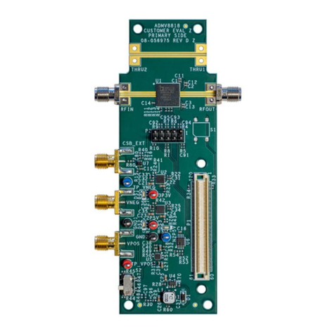
POWER SUPPLIES
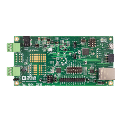
The EVAL-AD5753SDZ requires power supply inputs for the
AVDD1, AVDD2, AVSS, and VLOGIC supplies. If there is only one
positive rail available, connect the AVDD2 pin to the AVDD1 pin
via the AVDD1 -AVDD2-SHRT link. Select the VLOGIC supply from
the 3.3V_SDP evaluation board pin or the VLDO pin through the
VLOGIC_SOURCE link. See Table 1 for the default link positions
and see Table 2 for more linking options.
The EVAL-AD5753SDZ operates with a power supply range of
−33 V on AVSS to +33 V on AVDD1, with a maximum voltage of
60 V between the two rails. AVDD2 requires a voltage between
5 V and 33 V. To bypass the positive dc-to-dc circuitry, connect
the VDPC+ pin directly to AVDD1 via the JP6 jumper. To bypass the
negative dc-to-dc circuitry, connect the VDPC− pin directly to the
AVSS pin via the JP5 jumper. The recommended supply voltages are
AVDD2 = +5 V, AVDD1 = +24 V, and AVSS = −24 V.
SERIAL COMMUNICATION
The EVAL-SDP-CS1Z (SDP-S) handles communication to the
EVAL-AD5753SDZ via the PC. The EVAL-SDP-CS1Z (SDP-S)
handles the serial port interface (SPI) communication, controls
the RESET pin and the LDAC pin, and monitors the FAULT pin
of the AD5753.
Remove the appropriate links on P2 to disconnect the EVAL-
AD5753SDZ from the EVAL-SDP-CS1Z (SDP-S) and drive the
digital signals from an external source. The S1 link and the JP11
link allow the user to tie RESET and LDAC to high or low levels.
AD5753 ADDRESS PINS
The AD0 address pin and the AD1 address pin are used in
conjunction with the address bits within the SPI frame to
determine which AD5753 device is being addressed by the system
controller. Configure the AD0 pin and the AD1 pin through the
JP12 link and the JP14 link.
Table 1. EVAL-AD5753SDZ Link Option Functions
Link Default Position Function
AVDD1-AVDD2-SHRT Not inserted Connects AVDD2 to AVDD1.
VLOGIC_SOURCE A Position A selects 3.3 V from the EVAL-SDP-CS1Z (SDP-S). Position B selects 3.3 V from the VLDO
pin of the AD5753.
JP1 A
Position A powers the ADR4525 reference (ADR-REF) from the VLDO pin. Position B powers the
ADR-REF from AVDD2. The maximum supply for the ADR4525 is 15 V.
JP2 Inserted Selects the ADR-REF pin as the input to the REFIN pin.
JP4 Not inserted Selects the REFOUT pin as the input to the REFIN pin.
JP5 Not inserted Shorts the VDPC− pin to the AVSS pin to bypass the negative dc-to-dc circuitry.
JP6 Not inserted Shorts the VDPC+ pin to the AVDD1 pin to bypass the positive dc-to-dc circuitry.
JP7 Inserted Shorts the ADC2 pin to the +VSENSE pin.
JP8 Inserted Connects the VIOUT pin to the +VSENSE pin.
JP9 Not inserted Connects the RETURN signal to the GND position on the EVAL-AD5753SDZ.
JP10 Inserted Connects the −VSENSE pin to the RETURN signal.
JP11 A
Position A connects the LDAC pin to the GND position. Position B connects the LDAC pin to the
VLOGIC pin.
JP12 A
Position A connects the AD0 pin to the GND position. Position B connects the AD0 pin to the
VLOGIC pin.
JP13 B
Position A connects the GPIO_0 pin to the GND position. Position B connects the GPIO_0 pin to
the VLOGIC pin.
JP14 A
Position A connects the AD1 pin to the GND position. Position B connects the AD1 pin to the
VLOGIC pin.
JP15 B
Position A connects the GPIO_2 pin to the GND position. Position B connects the GPIO_2 pin to
the VLOGIC pin.
JP16 B
Position A connects the GPIO_1 pin to the GND position. Position B connects the GPIO_1 pin to
the VLOGIC pin.
JP17 Not inserted Connects the AVSS pin to the GND position for the unipolar supply option (current output only).
P2 Inserted
Provides options to disconnect from the EVAL-SDP-CS1Z (SDP-S) and to drive digital signals
from an external source. See Table 2 for the specific link options.
S1 2-3
Position 2-1 (on position to the right of off) connects the RESET pin to the GND position.
Position 2-3 (on position to the left of off) connects the RESET pin to the VLOGIC pin.

