UG-1060 EVAL-ADAQ7980SDZ User Guide
Rev. 0 | Page 10 of 30
For dynamic performance, conduct a fast Fourier transform
(FFT) test by applying a very low distortion ac source.
For low frequency testing, an instrument like an audio precision
source (such as the SYS-2700 series) can be used directly
because its outputs are isolated. Set the outputs as balanced with
a floating ground. The P3 and P4 connectors balance termination
of a signal source. Different sources can be used; however, most
are single-ended sources that use a fixed output resistance.
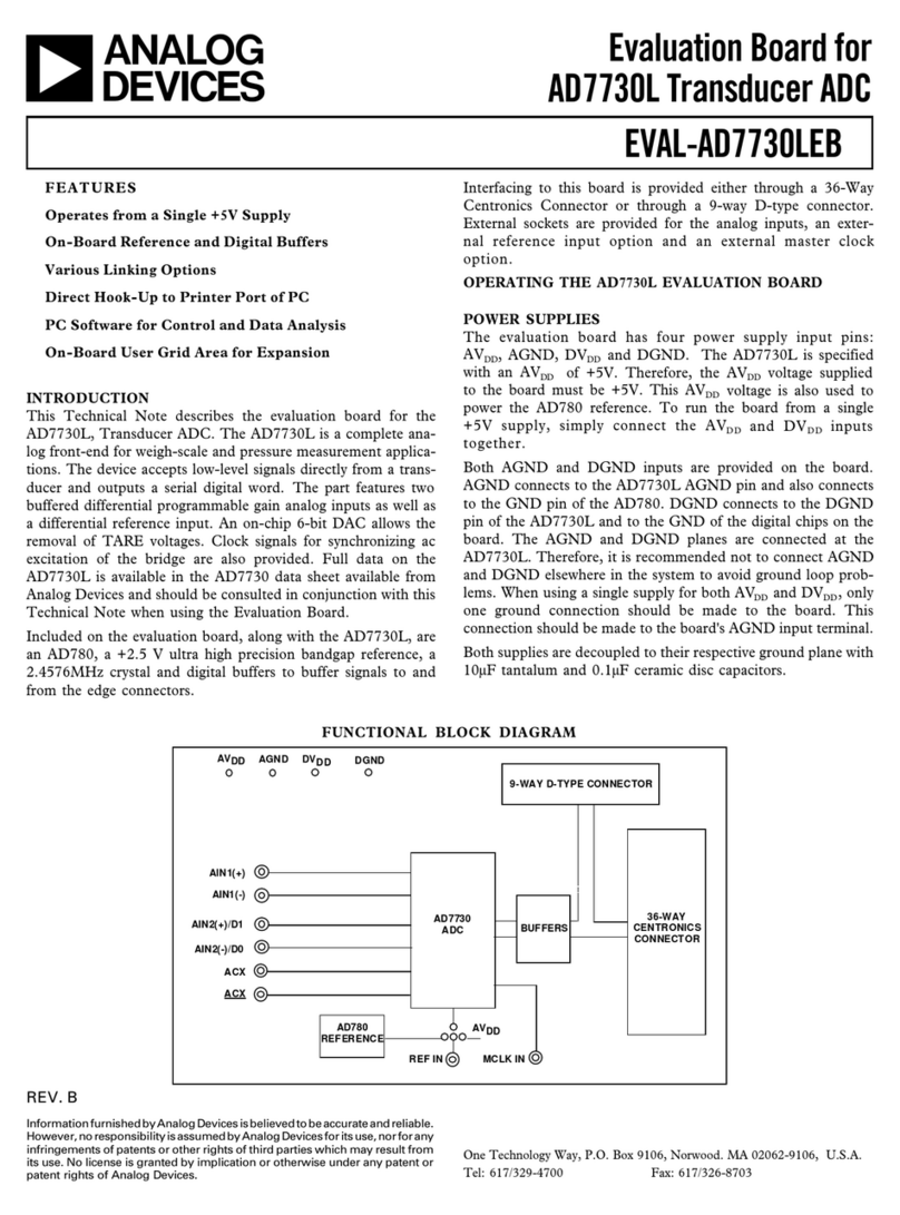
POWER SUPPLIES
The evaluation board can be powered from a wall adapter or from
a bench top power supply. By default, the EVAL-ADAQ7980SDZ
is set up to operate from a 9 V wall adapter using the on-board
power supplies described in Table 3.
Table 3. Power Supplies Provided on the
EVAL-ADAQ7980SDZ
Power Supply (V) Default Function
On-Board
Components
+7.5 V+ and VDD supply ADP7118
−2.5 V− supply ADP7182
+3.3 VDRIVE (VIO supply) ADP7118-3.3
Each on-board power supply is decoupled where it enters the
EVAL-ADAQ7980SDZ as well as at the power pins of each of the
on-board components. A single ground plane on the evaluation
board minimizes the effect of high frequency noise interference.
The EVAL-ADAQ7980SDZ provides multiple power scheme
options by means of various link settings on the evaluation
board. This allows evaluation of the ADAQ7980 with various
power configurations. By default, the EVAL-ADAQ7980SDZ is
configured as shown in Table 1. Table 4 lists the different supply
settings available.
Table 4. Alternate Power Supply Options
ADAQ7980
Power Pin Pin Function
On-Board Power
Options (V)
VDD Input to LDO powering
the ADC
+7.5 and +5
V+ ADC driver and reference
buffer positive supply
+7.5 and +5
V− ADC driver and reference
buffer negative supply
−2.5 and 0
To evaluate the ADAQ7980 in a single-supply configuration,
connect the V− pin to ground and connect the V+ and VDD
pins to either 7.5 V or 5 V. If V+ is set to 5 V, the device is not
able to use a 5 V reference voltage.
Alternatively, power the EVAL-ADAQ7980SDZ from a bench top
power supply by using the P6 terminal block. Individual supplies
can also be supplied externally through P6, but also require
changing the position of the relevant solder link (see Table 5).
When using bench top power, use of the wall adapter and the on-
board power supplies are no longer required.
Table 5. Solder Links—Settings for Bench Top Power Supply1
Link Setting Function
J17 3 +VS
J18 3 −VS
J13 3 V_SDP
J12 3 VDD
1See Table 6 for all other link settings.
DIGITAL INTERFACE
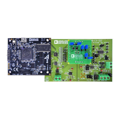
The evaluation board uses the synchronous serial peripheral
port (SPORT) interface from the ADSP-BF527 digital signal
processor (DSP) on the E VA L -SDP-CB1Z to control the digital
interface, for example, initiating conversion and data readback, of
the ADAQ7980. Multiple AND gates (U12, U13, and U14) clock
and gate the SPORT transfer to the ADAQ7980.
The evaluation board also provides optional connections between
the ADSP-BF527 DSP and the PD_REF and PD_AMP inputs
on the EVAL-ADAQ7980SDZ through Link J4 and J5,
respectively. These connections allow software controlled
dynamic power scaling (DPS) of the ADC driver and reference
buffer, which greatly reduces overall power consumption. For
more details on implementing DPS with the ADAQ7980,
consult the ADAQ7980/ADAQ7988 data sheet.
The ADAQ7980 PD_LDO input can also be connected to the
ADSP-BF527 DSP by means of Link J6. This is intended to
further reduce power consumption during long periods of
inactivity. Power cycling the ADAQ7980 integrated low dropout
regulator (LDO) requires a longer time than the ADC driver
and reference buffer, however, and may not be possible for
many DPS applications. See the ADAQ7980/ADAQ7988 data
sheet for power-down timing specifications for each of the
components.
