UG-875 EVAL-ADG5209FEBZ User Guide
Rev. 0 | Page 4 of 12
EVALUATION BOARD HARDWARE
The operation of the ADG5209F is evaluated using the E VA L -
ADG5209FEBZ. Figure 1 shows a typical evaluation setup
where only a power supply and signal generator are required.
Figure 2 shows the block diagram of the main components of
the evaluation board.
Using this evaluation board, the ADG5209F passes signals from
either the source or drain connectors. The source pins have fault
detection circuitry that react to an overvoltage event. During an
overvoltage event, the channel on which the fault occurs is
turned off. See the ADG5209F data sheet for more details.
POWER SUPPLY
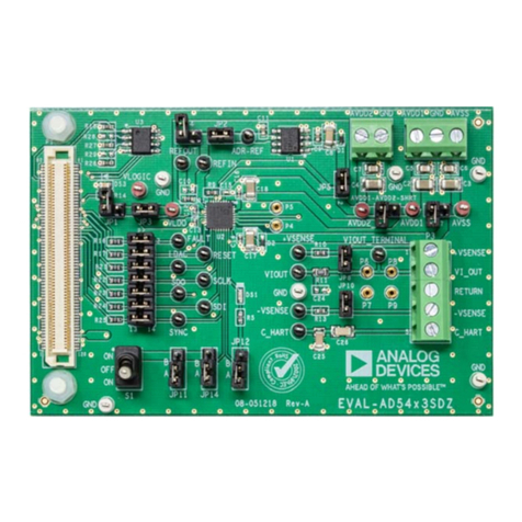
Connector J5 provides access to the supply pins of the
ADG5209F. VDD, GND, and VSS on J5 link to the appropriate
pins on the ADG5209F. For dual supply voltages, the evaluation
board can be powered from ±5 V to ±22 V. For single supply
voltages, the GND and VSS terminals must be connected together,
and power the evaluation board with 8 V to 44 V. Additionally,
an on-board LDO regulator is provided for a digital control
voltage. If necessary, a secondary voltage source can be
connected to EXT_VL and used to control the digital voltages.
To use EXT_VL, move the 0 Ω resistor from R14 to R13. Do not
expose the on-board LDO regulator to voltages greater than
28 V; remove R15 and supply an alternative digital voltage via
EXT_VL, if required.
INPUT SIGNALS
Four screw connectors are provided to connect to both
the source and drain pins of the ADG5209F. Additional
subminiature Version B (SMB) connector pads are available if
extra connections are required. The ADG5209F is overvoltage
protected on the source side, and each source terminal (S1A to S4A
and S1B to S4B) can be presented with a voltage of up to +55 V or
−55 V. See the ADG5209F data sheet for more details.
Each trace on the source and drain side includes two sets of
0603 pads, which can be used to place a load on the signal path
to ground. A 0 Ω resistor is placed in the signal path and can be
replaced with a user defined value. Use the resistor combined
with the 0603 pads to create a simple resistor-capacitor (RC)
filter.
The ADG5209F uses a parallel interface to control the operation of
the switches. The switch operation can be manually controlled
using the SW1 to SW3 switches, or an external controller can be
interfaced directly to the control pins by using the SMB connectors
(EN, A0, and A2) and removing the 0 Ω R31, R33, and R35
resistors.
