UG-900 EVAL-ADN4651EB1Z/EVAL-ADN4652EB1Z User Guide
Rev. A | Page 4 of 13
EVALUATION BOARD CONFIGURATION
SETTING UP THE EVALUATION BOARD
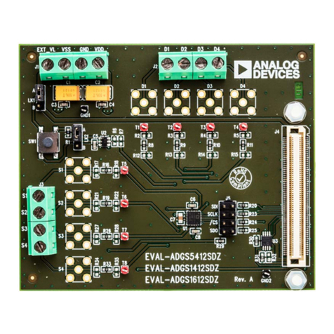
On the E VA L -ADN4651EB1Z/E VA L -ADN4652EB1Z, power
supplies are configured using Jumpers P4 and P7 (see Table 1)
and connected to the J9 and J10 SMA connectors (see Table 2 and
Table 3). A 3.3 V power supply can be applied to Side 1 and/or
Side 2 of the ADN4651/ADN4652 by removing Jumpers P4
(Side 1) and P7 (Side 2). If a 2.5 V supply is connected to the
board, the relevant jumper must be inserted (P4 for Side 1 and
P7 for Side 2). At 300 MHz with a load resistance of 100 Ω, the
maximum operating current from each power supply is 90 mA.
When using a 3.3 V power supply, VIN1and VDD1 (Pin 1 and Pin 3
on the ADN4651/ADN4652) are bypassed to GND1using 1 µF
capacitors. VIN2 and VDD2 (Pin 20 and Pin 18 on the ADN4651/
ADN4652) are bypassed to GND2using 1 µF capacitors. When
using a 2.5 V power supply, VIN1 or VIN2 is connected directly to
VDD1 or VDD2 by shorting Jumpers P4 or P7, respectively. Both
VDD1 pins are also bypassed to GND1with 0.1 µF capacitors. Both
VDD2 pins are also bypassed to GND2with 0.1 µF capacitors.
An example operation of the EVAL -ADN4651EB1Z is shown in
Figure 5 (signal generator and oscilloscope connections are
reversed for E VA L -ADN4652EB1Z, per Table 2 and Table 3).
SMA connectors expose all LVDS inputs and outputs for the
E VA L-ADN4651EB1Z, but are reversed for the E VA L -
ADN4652EB1Z (see Table 2 and Table 3). Connect a signal
generator to the board using the J1 and J2 connectors and set up
a 300 MHz square wave clock with an amplitude of 350 mV and
an offset of 1.2 V. Connect the oscilloscope directly to the J5
and J6 connectors to perform timing measurements including
propagation delay and skew. Precision measurements, for
example, jitter, using a differential probe requires attaching the
probe at the R7 or R3 resistors and potentially cutting the traces
to the connectors to minimize reflections.
A plot of the oscilloscope connected via the J5 and J6 connectors is
shown in Figure 3. Channel 3 (green) and Channel 4 (purple)
show the J5 and J6 connectors separately (single-ended) with
the differential signal (orange).
Operation of the second isolated LVDS channel is shown in
Figure 4. In contrast to Figure 5, the oscilloscope now connects
via the J3 and J4 connectors and the signal generator connects to
the J7 and J8 connectors. Channel 3 (green) and Channel 4
(purple) show the J3 and J4 connectors separately (single-ended)
with the differential signal (orange).
Figure 3. DOUT1− and DOUT1+ with a 300 MHz Clock, Single-Ended and Differential
Figure 4. DOUT2−and DOUT2+ with a 300 MHz Clock, Single-Ended and Differential
