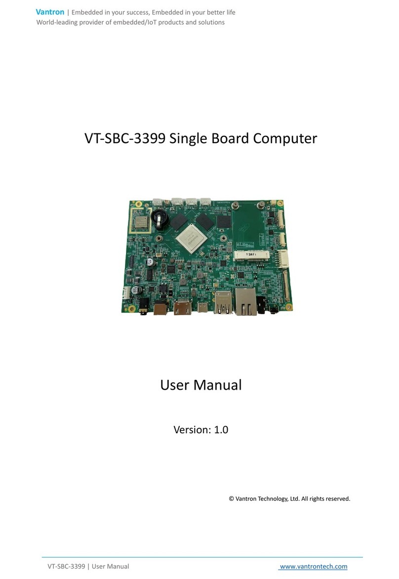
Arcom VIPER series User manual

VIPER
Intel PXA255 XScale RISC based
PC/104 Single Board Computer
Technical Manual
Product Information
Full information about other Arcom products is available by contacting our Website at: www.arcom.com
Useful Contact Information
Customer Support US Customer Support Europe
Tel: 913 549 1000
Fax: 913 549 1002
E-mail: [email protected]
Tel: +44 (0)1223 412 428
Fax: +44 (0)1223 403 409
E-mail:[email protected]
Sales offices Sales hotlines
United States:
Arcom
7500 West 161st Street
Overland Park
KS 66085, USA
Tel: 913 549 1000
Fax: 913 549 1002
E-mail:
United Kingdom:
Arcom
Clifton Road
Cambridge
CB1 7EA, UK
Tel: 01223 411 200
Fax: 01223 410 457
E-mail:
Belgium:
Groen Nummer:
Tel: 0800 7 3192
Fax: 0800 7 3191
France:
Numero Vert:
Tel: 0800 90 84 06
Fax: 0800 90 84 12
Germany:
Kostenlose Infoline:
Tel: 08001 824 511
Fax: 08001 824 512
Netherlands:
Gratis Nummer:
Tel: 0800 0221136
Fax: 0800 0221148
Italy:
Numero Verde:
Tel: 0800 790841
Fax: 0800 780841
Whilst Arcom’s sales team is always available to assist you in making your decision, the final
choice of boards or systems is solely and wholly the responsibility of the buyer. Arcom’s entire
liability in respect of the boards or systems is as set out in Arcom’s standard terms and
conditions of sale.
If you intend to write your own low level software, you can start with the source code supplied
by Arcom. This is example code only to illustrate use on Arcom’s products. It has not been
commercially tested. No warranty is made in respect of this code and Arcom shall incur no
liability whatsoever or howsoever arising from any use made of the code.
© 2003 Arcom Control Systems Ltd.
Arcom Control Systems is a subsidiary of Spectris plc
All trademarks recognized.
Arcom Control Systems Ltd
operate a company-wide quality
management system which has
been certified by the British
Standards Institution (BSI) as
compliant with ISO9001:2000

2192-12132-000-000
Contents
Contents......................................................................................................................................2
Revision History .........................................................................................................................3
Preface.........................................................................................................................................4
Definitions .................................................................................................................................4
Disclaimer .................................................................................................................................4
Anti-Static Handling...................................................................................................................4
Packaging .................................................................................................................................4
Electromagnetic Compatibility (EMC) .......................................................................................4
Acknowledgements...................................................................................................................4
Technical Support.....................................................................................................................5
Introduction.................................................................................................................................6
Features....................................................................................................................................7
VIPER-UPS (uninterruptible power supply)...........................................................................7
VIPER-ICE (industrial compact enclosure)............................................................................8
VIPER-FPIF1 (flat panel interface)........................................................................................8
Using the VIPER..........................................................................................................................9
Connecting a Host PC to the VIPER Console (COM1).........................................................9
Using the CompactFlash™ Socket......................................................................................10
Using the Serial Interfaces (RS232)....................................................................................10
Using the Audio Features....................................................................................................10
Using the PC/104 Expansion Bus .......................................................................................11
Using the USB Ports............................................................................................................11
Using the Ethernet Interface................................................................................................11
Jumpers and Connectors ........................................................................................................12
LK1 – Reset.........................................................................................................................13
LK2 – User Configurable Jumper 1.....................................................................................13
LK3 – User Configuration Jumper 2....................................................................................13
LK4, LK5, LK6 and LK7 – RS485/422 configuration ...........................................................13
Connectors..............................................................................................................................14
Bootloader.................................................................................................................................15
RedBoot..................................................................................................................................15
Detailed Hardware Description................................................................................................16
Processor................................................................................................................................16
Memory...................................................................................................................................16
Synchronous DRAM Interface.................................................................................................16
Bootloader EPROM.................................................................................................................17
Flash Memory/Silicon Disk......................................................................................................17
Static RAM..............................................................................................................................17
Memory Map...........................................................................................................................17
Graphics Controller.................................................................................................................18
Backlight Enable..................................................................................................................20
LCD Vcc Enable..................................................................................................................20
Backlight Brightness Control ...............................................................................................20
Interrupt Assignments.............................................................................................................20
Internal Interrupts ................................................................................................................20
External Interrupts...............................................................................................................20
PC104 Interrupts .................................................................................................................20
CompactFlash.........................................................................................................................21
Page 2

2192-12132-000-000
Real Time Clock......................................................................................................................21
Ethernet Controller..................................................................................................................22
Sound......................................................................................................................................22
Watchdog Timer......................................................................................................................22
User Configuration Jumpers ...................................................................................................22
USB Interface..........................................................................................................................22
General Purpose I/O...............................................................................................................23
PC/104 Interface.....................................................................................................................24
Serial Ports .............................................................................................................................24
COM1..................................................................................................................................24
COM2..................................................................................................................................24
COM3..................................................................................................................................24
COM4..................................................................................................................................24
COM5..................................................................................................................................24
RS422/485 Interfaces .............................................................................................................25
RS422.....................................................................................................................................25
RS485.....................................................................................................................................25
Power Supply..........................................................................................................................27
Power Management................................................................................................................27
Processor ............................................................................................................................27
UARTS ................................................................................................................................27
CompactFlash .....................................................................................................................28
Ethernet...............................................................................................................................28
USB.....................................................................................................................................28
Audio ...................................................................................................................................28
Status LED’s ...........................................................................................................................28
RESET Switch.........................................................................................................................28
Appendix A – Connector details .............................................................................................29
PL1 – 10/100M Ethernet .....................................................................................................29
PL3 - LCD Ports ..................................................................................................................29
PL4 – COMS Ports..............................................................................................................30
PL6 - Audio.........................................................................................................................30
PL7 - USB ...........................................................................................................................30
PL8 – CompactFlash...........................................................................................................31
PL9 - GPIO.........................................................................................................................31
PL10 – JTAG.......................................................................................................................32
PL10 & PL11 - PC/104 Connector.......................................................................................32
PL14 – Power 4-way Molex Mating Half – Molex 22-01-3047............................................33
Appendix B – Specification .....................................................................................................34
Appendix C - Mechanical Diagram..........................................................................................35
Appendix D - Reference Information ......................................................................................36
USB Information..................................................................................................................36
Intel......................................................................................................................................36
Revision History
Manual PCB Date Comments
Issue A
Issue B
Issue C
V1 Issue 3
V1 Issue 3
V1 Issue 4
26th June 2003
8th July 2003
14th August 2003
First full release of Manual
Minor Editorial Changes
Content update
Page 3

2192-12132-000-000
Preface
Definitions
Arcom is the trading name for Arcom Control Systems Inc and Arcom Control Systems Ltd.
Disclaimer
The information in this manual has been carefully checked and is believed to be accurate.
Arcom assumes no responsibility for any infringements of patents or other rights of third parties,
which may result from its use.
Arcom assumes no responsibility for any inaccuracies that may be contained in this document.
Arcom makes no commitment to update or keep current the information contained in this
manual.
Arcom reserves the right to make improvements to this document and /or product at any time
and without notice.
Anti-Static Handling
This board contains CMOS devices that could be damaged in the event of static electricity
discharged through them. At all times, please observe anti-static precautions when handling the
board. This includes storing the board in appropriate anti-static packaging and wearing a wrist
strap when handling the board.
Packaging
Please ensure that should a board need to be returned to Arcom, it is adequately packed,
preferably in the original packing material.
Electromagnetic Compatibility (EMC)
The VIPER is classified as a component with regard to the European Community EMC
regulations and it is the users responsibility to ensure that systems using the board are
compliant with the appropriate EMC standards.
Acknowledgements
ARM and StrongARM are registered trademarks of ARM Ltd.
Intel and XScale are trademarks or register trademarks of Intel Corporation or its subsidiaries in
the United States and other countries.
CompactFlash is the registered trademark of The CompactFlash Association.
Linux is a registered trademark of Linus Torvalds.
RedBoot and Red HatTM is a registered trademark of Red Hat Inc.
All other trademarks acknowledged.
Page 4

2192-12132-000-000
Technical Support
Arcom has a team of technical support engineers who will be able to provide assistance if you
have any problems with this product:
US
Europe [email protected] Tel +44(0) 1223 412 428
Page 5

2192-12132-000-000
Introduction
This manual describes the operation and use of the VIPER single board computer. It is
designed to be a reference and user manual and includes information on using all aspects of
the board.
This manual should have been supplied as part of a VIPER Development Kit and you should
have read the Quickstart Manual.
The VIPER is an ultra low power PC/104 compatible single board computer based on the Intel
400MHz PXA255 XScale processor. The PXA255 is an implementation of the Intel XScale
micro architecture combined with a comprehensive set of integrated peripherals including, a flat
panel graphics controller, DMA controller, interrupt controller, real time clock and multiple serial
ports. The VIPER board offers a wide range of features making it ideal for power sensitive
embedded communications and multimedia applications.
The board is available in the following standard variants:
VIPER-400-M64-F16 Intel XscaleTM PXA255 400MHz CPU, 64MByte DRAM, 16MByte Flash
VIPER-400-M16-F8 Intel XscaleTM PXA255 400MHz CPU, 16MByte DRAM, 8MByte Flash
Page 6

2192-12132-000-000
Features
• CPU:
Intel XScaleTM PXA255 400MHz RISC processor
• Cache:
32k data cache, 32k instruction cache
• System Memory:
Up to 64MByte un-buffered 3.3V SDRAM
• Silicon Disk:
Up to 16MByte Intel Strata Flash (with Flash access LED)
1MByte Flash EPROM for RedBoot (with Flash access LED)
256Kbyte SRAM (with external battery backup)
• Video:
TFT/STN (3.3V or 5V – factory fit) flat panel graphics controller, Up to 800X600,
Backlight Control.
• Audio:
National Semiconductors LM4548 CODEC
Line IN, Line OUT, Microphone and 200mW per channel amplified output
• Serial Ports:
5x 16C550 compatible high speed UART’s
2x channels with 128byte Tx/Rx FIFO
4 x RS232 and 1 x RS422/485 Interfaces
• USB Host Interface:
Two Universal Serial Bus (USB) interfaces
USB 1.1 Compliant
• Network support:
SMSC SMC91C111 10/100-BASETX Ethernet controller
• Real Time Clock (RTC):
Battery backed RTC (external battery)
• Watchdog:
Adjustable timeout of 271µs – 17s
• General Purpose I/O (GPIO):
8 x 5V tolerant Inputs
8 x 3.3V Outputs (5V tolerant)
• 2x User Jumpers:
• Expansion:
PC/104 expansion bus - 8/16 bit ISA bus compatible interface
• JTAG Port:
Download data to Flash memory
Debug and connection to In-Circuit Emulator (ICE)
• Size:
PC104 Compatible footprint 3.8” x 3.6” (96mm x 91mm)
The VIPER SBC is supported by the following products:
VIPER-UPS (uninterruptible power supply)
The VIPER-UPS serves as a 5V DC power supply and battery back up system for the VIPER
SBC. The UPS accepts between 10 – 36 VDC (10-25VAC) input and generates the +5V supply
for the VIPER. In addition to this, it includes an intelligent battery charger/switch capable of
Page 7

2192-12132-000-000
using either the onboard 500mAHr NiMH battery or an external sealed lead acid rechargeable
battery.
VIPER-ICE (industrial compact enclosure)
The VIPER-ICE is a simple low cost aluminum enclosure which provides easy connection to all
on board features. The enclosure includes the VIPER-UPS and optionally a color Q-VGA
(320x240) flat panel display and analog touch screen.
VIPER-FPIF1 (flat panel interface)
The VIPER-FPIF1 is a simple board to enable easy connection between the VIPER SBC and
an LCD flat panel.
Page 8

2192-12132-000-000
Getting Started
The Development Kit contains a Quickstart Manual to enable users to set-up and start using the
board. Please read this manual and follow the steps defining the set-up of the board. Once you
have completed this task you will have a working VIPER system and can start adding further
peripherals enabling development to begin.
The section below has been designed as a guide to the set-up and use of some of the features
of the VIPER. If you would like more detailed information on any aspect of the board refer to the
“Detailed Hardware Description” section of this manual.
Using the VIPER
The VIPER uses the RedBoot bootloader (Red Hat Embedded Debug and Bootstrap firmware)
to provide initial boot strapping for the board. The bootloader has many features including:
Downloading and execution of embedded operating systems via a serial port (X or Y modem),
or Ethernet (support for BOOTP and TFTP).
Interactive command line interface allows management of Flash images, downloads and
general configurations.
RedBoot only has limited support for the VIPER hardware (Ethernet, Serial, Flash, SDRAM), to
use any other hardware function an operating system and appropriate drivers must be running.
Connecting a Host PC to the VIPER Console (COM1)
RedBoot does not support the flat panel controller, therefore by default the console is directed
to COM1. To view this you will need a null modem cable, which is supplied in the Development
Kit and a computer with a suitable terminal emulator. Connect one end of the null modem cable
to the VIPER’s COM1 and the other to your computer. Set the terminal emulator as follows:
Baud Rate: 115200
Data Bits: 8
Parity: None
Stop Bits: 1
Flow Control: None
Plug the power supply into the VIPER. You should now see the following in your terminal
emulator window:
Ethernet eth0: MAC address 00:80:66:10:00:01
IP: 10.2.28.4/255.255.0.0, Gateway: 10.2.1.1
Default server: 10.2.28.2, DNS server IP: 0.0.0.0
RedBoot(tm) bootstrap and debug environment [ROM]
Non-certified release, version @CURRENT@ for VIPER - built 11:40:34, Apr 16 2003
Platform: VIPER (XScale PXA255)
Copyright (C) 2000, 2001, 2002, Red Hat, Inc.
RAM: 0x00000000-0x04000000, 0x00013ca8-0x03fdd000 available
FLASH: 0x60000000 - 0x61000000, 128 blocks of 0x00020000 bytes each.
RedBoot>
Page 9

2192-12132-000-000
Required null modem cable pin out:
9 Way D-Sub (Female) 9 Way D-Sub (Female)
2 3
3 2
5 5
Using the CompactFlash™ Socket
The VIPER is fitted with a Type II CompactFlash socket mounted on the topside of the board.
This socket is connected to Slot 0 of the PXA255 PC Card interface. The socket supports both
Type I and Type II CompactFlash cards, for both memory and IO. The VIPER supports hot
swap changeover of the cards and notification of card insertion.
The CompactFlash card can only be inserted into the socket one way. The correct orientation is
for the top of the card i.e. the normal printed side to be face down to the PCB.
RedBoot does not support the CompactFlash interface, so a suitable operating system such as
Arcom Embedded Linux (AEL) port or Windows CE .NET, will need to be installed to support
this function.
Using the Serial Interfaces (RS232)
The five serial port interfaces on the VIPER are fully 16550 compatible. Connection to the serial
ports is made via a 40-way boxed header. The pin assignment of these headers has been
arranged to enable a 9-way IDC D-Sub plug to be connected directly to the cable. The D-Sub
connector will be compatible with the standard 9-way connector on a desktop computer. A
suitable cable is provided as part of the Development Kit.
Using the Audio Features
There are four audio interfaces supported on the VIPER, Amp out, Line out, Line in and
Microphone. The Line In, Line Out and Amp interfaces support stereo signals and the
Microphone provides a Mono input. The amplified output is suitable for direct drive of any 4-8Ω
load with a maximum power output of 2mW per channel. Connections are routed to a 12-way
header PL6. The relevant signals for each interface are shown in the table below:
Function Pin No. Signal
9 MICMicrophone 7 Audio ground reference.
1 Line input Left
5 Line input Right
Line IN
3 Audio ground reference
2 Line output Left
6 Line output Right
Line OUT
4 Audio ground reference
Amp OUT 8 Amp output Left
12 Amp output Right
10 Audio ground reference
Page 10

2192-12132-000-000
Using the PC/104 Expansion Bus
PC/104 modules can be used with the VIPER to add extra functionality to the system. This
interface supports 8/16 bit ISA bus style peripherals.
Arcom has a wide range of PC/104 modules which are compatible with the VIPER, these
include modules for digital I/O, analog I/O, motion control, video capture, CAN bus, serial
interfaces etc. Please contact the Arcom sales team if a particular interface you require does not
appear to be available as these modules are in continuous development.
In order to use a PC/104 board with the VIPER it should be plugged into PL11 for 8-bit cards
and PL11/PL12 for 8/16-bit cards. Before powering up the system, check that the jumper
settings on the card for I/O address and IRQ settings do not conflict with any devices on the
VIPER. The ISA interface on the VIPER does not support DMA. Please refer to the Interrupt
Assignment section of this manual fort PC/104 interrupts use.
If a PC/104 card that requires +5V is used, this will automatically be supplied via the PC/104
header. If +12V required this will only be available if the +12V pin on the ‘POWER’ connector
PL16 has been connected to a supply. If –12V or –5V are required, these must be supplied
directly to the PC/104 add-on board.
The VIPER is available with non-stackthrough connectors by special order. Contact the Arcom
sales for more details.
Using the USB Ports
The standard USB connector is a 4-way socket, which provides power and data signals to the
USB peripheral. The 10-way header PL7 has been designed to be compatible with PC
expansion brackets that support two USB sockets ( please refer to the USB section in this
manual and Appendix A for further details).
Using the Ethernet Interface
The SMSC LAN91C111 10/100baseTx Ethernet controller is configured by the RedBoot
bootloader. Connection is made via the 8-way header PL1. A second connector PL2 provides
outputs that can be used to control LED's for Activity and Link status (refer to Appendix A for pin
out details of this connector).
Page 11

2192-12132-000-000
Jumpers and Connectors
There are seven user selectable jumpers on the VIPER. The following section provides details
on these jumpers. The ‘+’ sign indicates the default position for each jumper. The jumpers are
also shown in the default position below:
Page 12

2192-12132-000-000
LK1 – Reset
A momentary switch (push to make) may be connected to LK1, when the button is pressed it will
put the board into a full hardware reset. Once the jumper is open circuit, the board will start
executing from the top of memory.
LK2 – User Configurable Jumper 1
This jumper has no reserved function on the VIPER, but can be used by an application program
to signify a configuration setting.
LK2 Description
Fit+ Read as ‘0’
Omit Read as ‘1’
LK3 – User Configuration Jumper 2
This jumper has no reserved function on the VIPER, but can be used by an application program
to signify a configuration setting.
LK2 Description
Fit+ Read as ‘0’
Omit Read as ‘1’
LK4, LK5, LK6 and LK7 – RS485/422 configuration
These jumpers are used to configure the RS485/422 serial interface. They can be used to
enable/disable the RS485 receive buffer and RS485/422 line termination (see the RS485/422
section for more details).
LK4 Description
Fit+ RS422 TX line termination resistor (120Ω) connected
Omit RS422 TX line termination resistor (120Ω) disconnected
LK5 Description
Fit+ RS485 (RS422 RX line) termination resistor (120Ω) connected
Omit RS485 (RS422 RX line) termination resistor (120Ω) disconnected
LK6 &
LK7 Description
A+ RS485 Half-duplex
B RS422 Full-duplex
Page 13

2192-12132-000-000
Connectors
There are 13 connectors on the VIPER that allow you to connect external devices such as
serial, CompactFlash, USB, audio etc. Detailed pin assignments are shown in Appendix A.
Connector Description
PL1 Ethernet Controller Status LED’s
PL2 Ethernet Interface
PL3 LCD Panel Interface
PL4 Serial Ports
PL5 Link Header
PL6 Audio
PL7 USB
PL8 CompactFlash
PL9 GPIO
PL10 JTAG
PL11 64-way PC/104 Expansion
PL12 40-way PC/104 Expansion
PL13 Factory use only
PL14 Power / Battery
Page 14

2192-12132-000-000
Bootloader
The VIPER is normally supplied with the RedBoot bootloader.
RedBoot
A list of available commands and thier syntax can be obtained by typing help at the RedBoot
prompt:
RedBoot> help
Manage aliases kept in FLASH memory
alias name [value]
Set/Query the system console baud rate
baudrate [-b <rate>]
Manage machine caches
cache [ON | OFF]
Display/switch console channel
channel [-1|<channel number>]
Compute a 32bit checksum [POSIX algorithm] for a range of memory
cksum -b <location> -l <length>
Display (hex dump) a range of memory
dump -b <location> [-l <length>] [-s] [-1|2|4]
Execute an image - with MMU off
exec [-w timeout] [-b <load addr> [-l <length>]]
[-r <ramdisk addr> [-s <ramdisk length>]]
[-c "kernel command line"] [<entry_point>]
Manage FLASH images
fis {cmds}
Manage configuration kept in FLASH memory
fconfig [-i] [-l] [-n] [-f] [-d] | [-d] nickname [value]
Execute code at a location
go [-w <timeout>] [entry]
Help about help?
help [<topic>]
Set/change IP addresses
ip_address [-l <local_ip_address>] [-h <server_address>]
Load a file
load [-r] [-v] [-h <host>] [-m <varies>] [-c <channel_number>]
[-b <base_address>] <file_name>
Compare two blocks of memory
mcmp -s <location> -d <location> -l <length> [-1|-2|-4]
Fill a block of memory with a pattern
mfill -b <location> -l <length> -p <pattern> [-1|-2|-4]
Network connectivity test
ping [-v] [-n <count>] [-l <length>] [-t <timeout>] [-r <rate>]
[-i <IP_addr>] -h <IP_addr>
Reset the system
reset
Display RedBoot version information
version
Display (hex dump) a range of memory
x -b <location> [-l <length>] [-s] [-1|2|4]
RedBoot>
Page 15

2192-12132-000-000
For information on each command and examples of using them, please refer to the RedBoot
section (Chapter 2) of the eCos Users Manual that is supplied on the VIPER Development Kit
CD. Not all commands that are listed in the manual are supported, only those that are listed in
the table above.
Detailed Hardware Description
The following section provides a detailed description of the functions provided by the VIPER.
This information may be required during development after you have started adding extra
peripherals or are starting to use some of the embedded features.
Processor
The PXA255 is a low power ARM (version 5TE) instruction set compliant RISC processor. The
PXA255 does not include a floating-point unit, however, the device contains a DSP co-
processor to enhance multimedia applications. The 400MHz PXA255 is driven by a 3.6864 MHz
clock, which is then used to generate all the high-speed clocks within the device.
The processor has two supply inputs: the core is powered from a +0.8 – 1.3V source and the
I/O is powered from +3.3V. These voltages are generated on the VIPER from the main +5V
supply input.
The PXA255 provides a Synchronous DRAM controller, 16-bit flat panel interface, AC97
interface, PC card / CompactFlash interface and a USB client controller.
The PXA255 processor is packaged in 256 ball PBGA, and therefore is attached to the board
during the assembly process.
The PXA255 processor is a low power device so a heat sink is not required to support ambient
temperatures up to 70°C (85°C for the industrial variant).
Memory
The VIPER includes four types of memory device, the synchronous DRAM system memory,
1MByte bootloader EPROM, the resident Flash array and 256KBytes of SRAM.
Synchronous DRAM Interface
There are two memory configurations supported by the VIPER, these are 16Mbyte and
64MByte of SDRAM. These are surface mount devices soldered to the board and cannot be
upgraded. Regardless of the variant, all of the SDRAM is located in DRAM BANK 0. RedBoot
automatically detects the amount of memory fitted to the board, and configures the SDRAM
controller accordingly.
The SDRAM controller supports running the memory at frequencies between 50MHz and
100MHz, this can be configured to achieve the optimum balance between power consumption
and performance.
Page 16

2192-12132-000-000
Bootloader EPROM
A 1MByte Flash EPROM device is used as the boot ROM and serves as a location for RedBoot
and configuration information.
Flash Memory/Silicon Disk
The VIPER supports up to 16MByte Flash memory, using the PXA255 CS1 to access the
devices, the Flash is located at address 0x04000000. The Flash status LED will illuminate
whenever the Flash drive is accessed. The Flash memory ‘busy’ status output can be read from
I/O line GP14 of the PXA255, this can be used to generate an interrupt to indicate the
completion of a CFI (Common Flash Interface) command.
Static RAM
The VIPER is designed to support a 256KByte static RAM device. The static RAM device can
be backed up from an off board battery when the main supply is removed, therefore data will be
non-volatile. The SRAM uses the PXA255 CS5 to access the device, and is offset by 8MByte in
the chip select; (located at 0x1480 0000).
Memory Map
The following table shows the memory map for the VIPER. These are the physical memory
locations before any translation by the MMU (Memory Management Unit):
Address Description
0xA000 0000 – 0xA3FF FFFF SDRAM
0x4C00 0000 – 0x9FFF FFFF Reserved
0x4800 0000 – 0x4BFF FFFF Memory Control Registers*
0x4400 0000 – 0x47FF FFFF LCD Control Registers*
0x4000 0000 – 0x43FF FFFF PXA 255 Peripherals*
0x3000 0000 – 0x3FFF FFFF PC104 (memory and I/O space)
0x2000 0000 – 0x2FFF FFFF CompactFlash
0x1484 0000 – 0x1FFF FFFF Reserved
0x1480 0000 – 0x1483 FFFF SRAM
0x1450 0002 – 0x2FFF FFFF Reserved
0x1450 0000 – 0x1450 0001 General Purpose Input
0x1430 0020 – 0x144F FFFF Reserved
0x1430 0010 – 0x1430 001F COM4 (external 16C2852 UART)
0x1430 0000 – 0x1430 000F COM5 (external 16C2852 UART)
0x1400 0000 – 0x142F FFFF Reserved
0x1000 0008 – 0x13FF FFFF Reserved
0x1000 0000 – 0x1000 0004 Ethernet Data port (CS4)
0x0C00 0006 – 0x0FFF FFFF Reserved
0x0C00 0000 – 0x0C00 0004 USB Host Controller (CS3)
0x0800 0310 – 0x0FFF FFFF Reserved
0x0800 0300 – 0x0800 030F Ethernet Register Space (CS2)
0x0800 0000 – 0x0800 02FF Reserved
0x0400 0000 – 0x07FF FFFF Reserved
0x0400 0000 – 0x04FF FFFF Flash Array (CS1)
0x0010 0000 – 0x03FF FFFF Reserved
0x0000 0000 – 0x000F FFFF Boot Rom (CS0)
Page 17

2192-12132-000-000
*More details of the internal registers are in the Intel Developer Manual on the Development Kit
CD.
The following table shows the translations made by the MMU under RedBoot:
Device Size Physical Virtual
Boot Rom (CS0) 1MByte 0x0 0x5000 0000
SDRAM 64MByte 0xA000 0000 0x0
Flash Array 64MByte 0x0400 0000 0x6000 0000
Cache Flush 128MByte N/A 0xE000 0000
Ethernet, USB, SRAM, UARTs, CompactFlash, PC104 and all internal registers are the physical
address location.
Graphics Controller
The Intel PXA255 processor contains a 16-bit flat panel display controller and provides an
interface capable of driving passive (STN) or active (TFT) flat panel displays. A full explanation
of the graphics controller operation can be found in the PXA255 data sheets included on the
support CD. The flat panel data and control signals are routed to a 40-way high-density
connector (PL3). The flat panel interface can be configured to drive a variety of panel types.
The part number for the flat panel interface connector is: Oupiin 3214-40RB
The mating connector is part number: Oupiin 1203-40GB
The VIPER-FPIF is available which allows the user to easily wire-up a new panel using pin and
crimp style connectors.
The following tables provide a cross-reference between the flat panel output signals and their
function when configured for different displays.
9-Bit TFTPanel Data
Bus Bit 18-Bit TFT 12-Bit TFT
FPD 15 R5 R3 R2
FPD 14 R4 R2 R1
FPD 13 R3 R1 R0
FPD 12 R2 R0
FPD 11 R1
GND R0
FPD 10 G5 G3 G2
FPD 9 G4 G2 G1
FPD 8 G3 G1 G0
FPD 7 G2 G0
FPD 6 G1
FPD 5 G0
FPD 4 B5 B3 B2
FPD 3 B4 B2 B1
FPD 2 B3 B1 B0
FPD 1 B2 B0
FPD 0 B1
GND B0
Page 18

2192-12132-000-000
Dual ScanPanel Data
Bus Bit Dual Scan
Colour STN Single Scan
Colour STN Mono STN
FPD 15 DL6(G)
FPD 14 DL6(R)
FPD 13 DL5(B)
FPD 12 DL4(G)
FPD 11 DL3(R)
FPD 10 DL2(B)
FPD 9 DL1(G)
FPD 8 DL0(R)
FPD 7 DU7(G) D7(G) DL3
FPD 6 DU6(R) D6(R) DL2
FPD 5 DU5(B) D5(B) DL1
FPD 4 DU4(G) D4(G) DL0
FPD 3 DU3(R) D3(R) DU3
FPD 2 DU2(B) D2(B) DU2
FPD 1 DU1(G) D1(G) DU1
FPD 0 DU0(R) D0(R) DU0
Below is a table covering the clock signals required for passive and active type displays:
VIPER Pin Active Display
Signal (TFT) Passive Display Signal
(STN)
PCLK Clock Pixel Clock
LCLK Horizontal Sync Line Clock
FCLK Vertical Sync Frame Clock
BIAS DE (Data Enable) Bias
The display signals are +3.3V compatible; the VIPER contains power control circuitry for the flat
panel logic supply and backlight supply. The flat panel can be supplied with a switched 3.3V
supply while the backlight can be supplied with a switched 5V supply. As there is no on-board
protection for these switched supplies, care should be taken not to draw too much current
(Refer to the Power Supply section for details).
Care must be taken during power up/down to ensure the panel is not damaged due to the input
signals being incorrectly configured. Typically the power up and power down sequence is as
follows, please check the datasheet for the particular panel in use.
Power Up:
1. Enable Display VCC
2. Enable Flat panel interface
3. Enable Backlight
Power Down is in reverse order.
Page 19

2192-12132-000-000
The following PXA255 GP lines are used for LCD functions.
PXA255 GP Function
GP9 Backlight Enable
GP10 LCD Vcc Enable
GP16 (PWM0) Backlight brightness control
Backlight Enable
This controls the switched backlight supply voltage. When the GP9 is set to a logic high the
backlight supply is turned on BLKSAFE (PL3 – Pin 2). The BLKEN signal on PL3 (pin 1) is the
un-buffered GP9 signal.
LCD Vcc Enable
This controls the switched LCD supply voltage when the GP10 is set to a logic high the LCD
supply is turned on LCDSAFE (PL3 – Pin 6). The default LCD output supply is 3.3V.
Note: This may be factory configured (using a surface mount resistor) to 5V.
Backlight Brightness Control
GP16 is available on PL3, pin 7. This can be used in one of two ways, dependant upon the type
of backlight inverter being used. Some inverters have a ‘DIM’ function, a logic level to choose
between two levels of intensity, if this is the case GP16 can be used to set this. Other inverters
have an input suitable for a PWM (Pulse Width Modulation); in this case GP16 can be
configured as PWM0.
Interrupt Assignments
Internal Interrupts
For details on the PXA255 interrupt controller and internal peripheral interrupts please refer to
the Intel PXA255 developer’s manual on the Development Kit CD.
External Interrupts
The following table lists the GP lines used for generating interrupts externally to the PXA255:
PXA255 GP Peripheral
GP0 Ethernet
GP1 PC104 Interrupt Controller
GP2 USB
GP3 COM4
GP4 COM5
GP8 CompactFlash RDY/nBSY
GP14 FLASH
GP32 CompactFlash Card Detect
PC104 Interrupts
Any interrupt generated on the PC104 interface will generate an interrupt using GP1 in a level
triggered mode. A register located at 0x30000000 will indicate which PC104 IRQ generated the
interrupt. The register indicates the status of the interrupt lines at the time the register is read,
the relevant bit is set to a 1.
Page 20
This manual suits for next models
2
Table of contents
