Arena 3P3 User manual

1
UNINTERRUPTIBLE POWER SYSTEM
SERVICE MANUAL
Arena 3P3&3P1&1P1 6-10KVA RT Model
Rev. 1.0

2
Table of contents
1. General information .......................................................................................................................................... 3
1.1 Getting start ........................................................................................................................................... 3
1.2 Important safety instructions ............................................................................................................... 3
2. Electric Specifications ...................................................................................................................................... 4
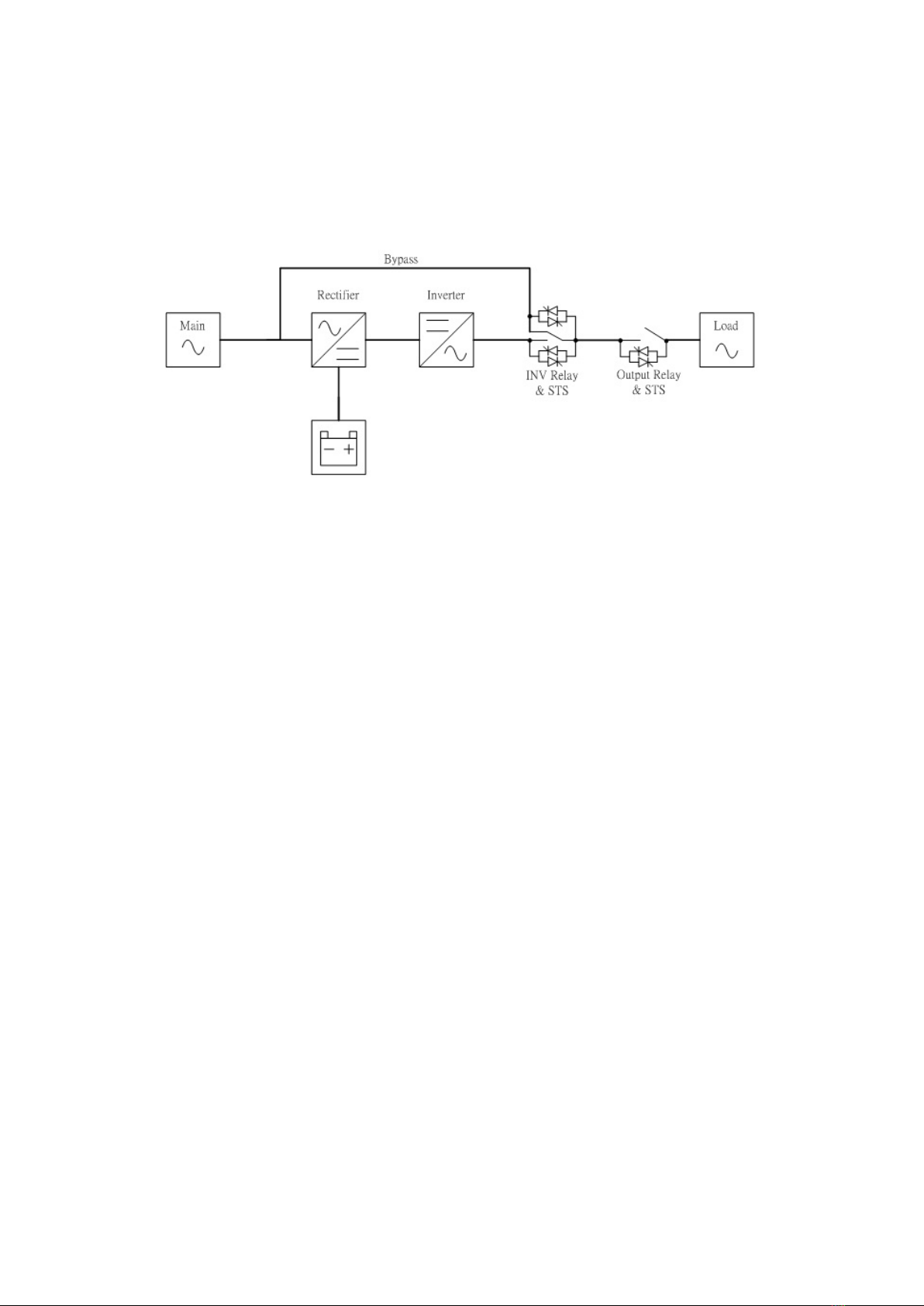
3. Functional block ................................................................................................................................................ 6
4. Working principle of the major functional block ............................................................................................ 7
4.1 Switch Power Supply ............................................................................................................................ 7
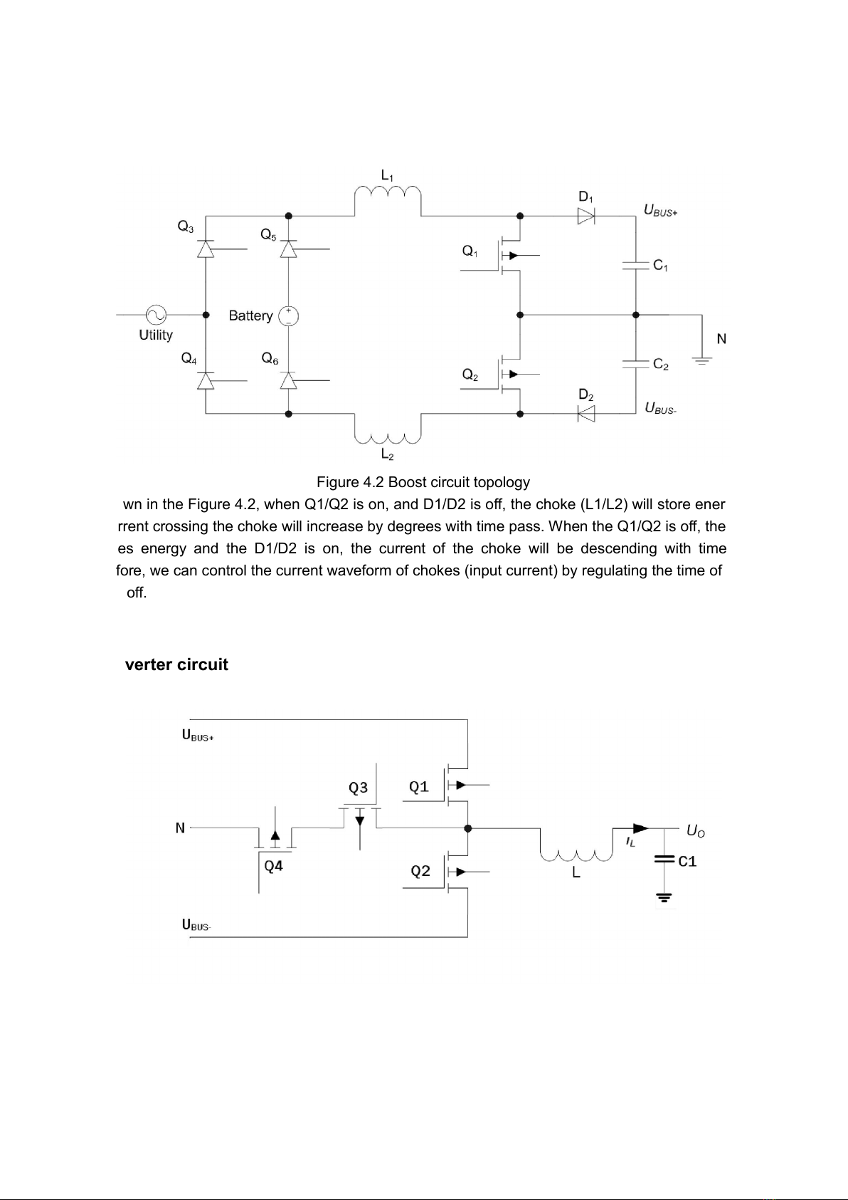
4.2 PFC/Boost circuit .................................................................................................................................. 8
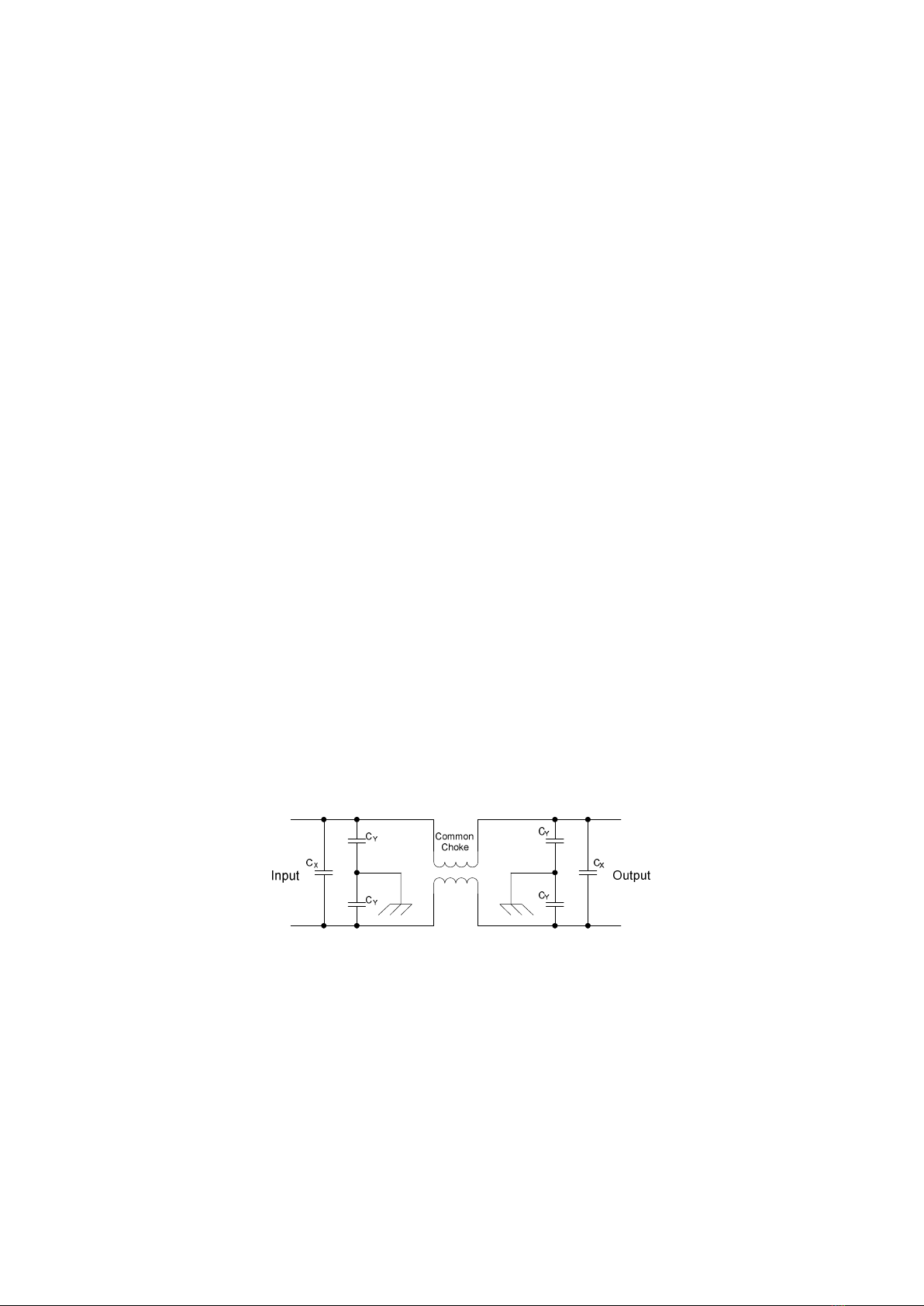
4.3 Inverter circuit ........................................................................................................................................ 8
4.4 Charger ................................................................................................................................................... 9
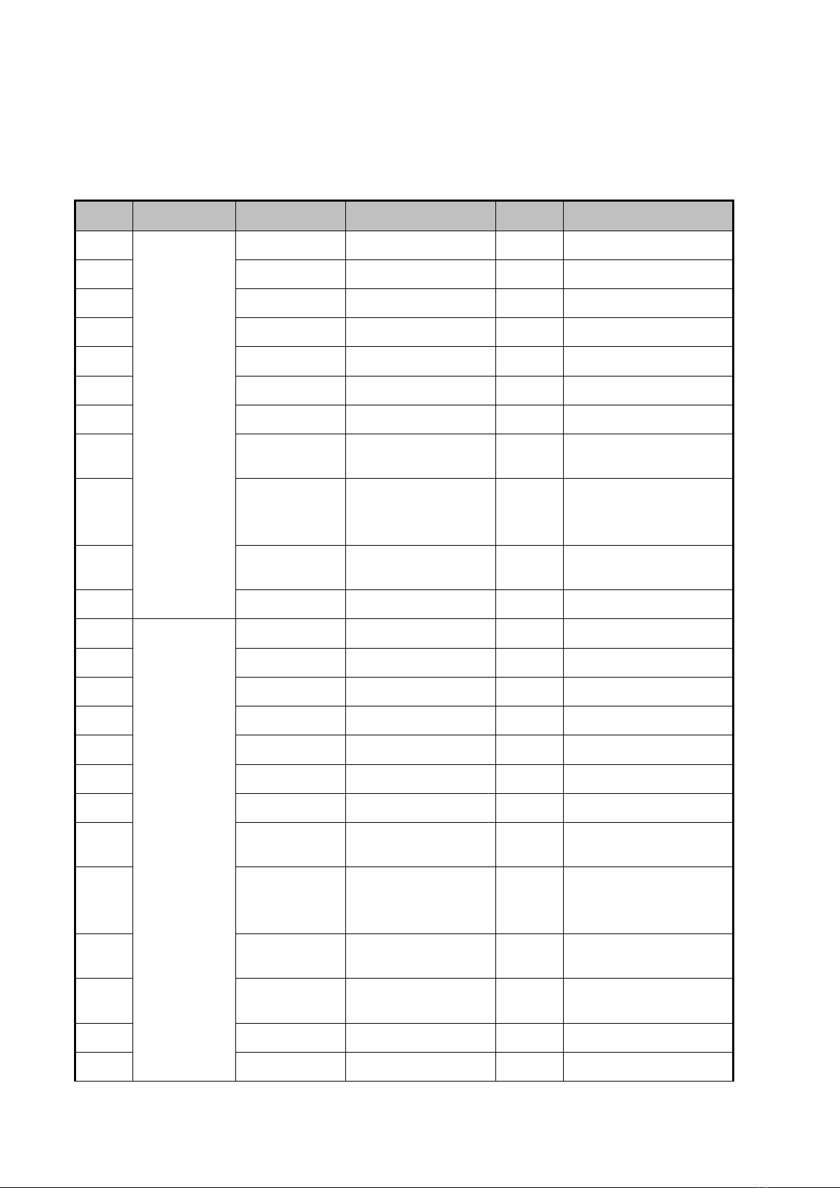
4.5 EMI Board .............................................................................................................................................. 9
5. Functional explanations for each PCB ......................................................................................................... 10
5.1 PFC board (Power Factor Correct Board) ....................................................................................... 12
5.2 INV board (Inverter Board) ................................................................................................................ 13
5.3 Charge board ....................................................................................................................................... 15
5.4 CNTL board (Control board) .............................................................................................................. 15
5.5 BUS board ............................................................................................................................................ 16
5.6 SPS board (Switch power supply) .................................................................................................... 17
5.7 IPOP EMI board .................................................................................................................................. 17
5.8 EPO and Communication board ....................................................................................................... 18
5.9 SYS LCD Panel board ........................................................................................................................ 19
5.10 SWITCH board .................................................................................................................................... 20
6. Interface ............................................................................................................................................................ 21
6.1 Button Operation ................................................................................................................................. 21
6.2 LED display .......................................................................................................................................... 21
6.3 LCD Display ......................................................................................................................................... 22
7. Trouble Shooting ................................................................................................................................. 24
7.1 Warning status ......................................................................................................................... 24
7.2 Fault mode ............................................................................................................................... 24
7.3 Trouble shooting table .............................................................................................................. 25
7.4 Failure Shooting ....................................................................................................................... 29
7.5 Quick start ................................................................................................................................ 31
8 Test Step ............................................................................................................................................. 34

3
1. General information
1.1 Getting start
This manual is for Arena 3/3&3/1&1/1 10K(L) RT UPS. It can help service person perform the basic
maintenance and repair service.
This manual only focuses on the service section, so you should get the basic operation of the UPS from
the user manual, and make sure you had read and understood the user manual before reading the
manual.
The manual include 8 sections, as follows
General Information, this
section show you the general information of the service manual
Functional Block, this section show you the major functional block of the UPS
Working Principle of the major Functional Block, this section show you the major functional block
Function explanations for each PCB, this section show you all the PCBs of the UPS
Interface, this section show you the LCD interface, include display and setting
Trouble shooting, this section will give you the way to find the trouble
Test step ,this section tell you how to test the UPS after you repair the unit
Electric Specifications, this section show you the basic electric specification of the UPS
1.2 Important safety instructions
WARNING: This chapter contains important safety and operating instructions. Read and keep this
manual for future reference.
For qualified service personnel only.
DO NOT performs any internal service or adjustment of this product unless another person is
capable of rendering first aid and resuscitation is present.
Dangerous voltage exists at several points in this product. To avoid personal injury, don't touch
any exposed connections or components while UPS is on.
Turn off the UPS and switch off the input breaker before removing outside protective cover.
AC voltage is always present if the input AC power is still available.
High voltage may present at DC capacitors. Before opening the outside cover, wait for at least five
minutes after turning off the UPS.
Verify input source (voltage and frequency) is within the maximum range before service.

4
2. Electric Specifications
MODEL SPECIFICATION
1P1 10K(L) 3P1 10K(L) 3P3 10K(L) 2P2 6K(L)
Input
Input Voltage 176~276 VAC(L-N)@ Full Load 88~155
VAC(L-N)
110~300 VAC(L-N) @ Half Load
Input Frequency 46~54 Hz for 50Hz system
56~64 Hz for 60Hz system
Input Power Factor
0.99 @100% R/RCD Load
0.97 @ 50% R/RCD Load
Input THD(Full Load) <4%@ Linear load
<5%@ Linear load
<4%@ Linear load
<4%@ Linear load
Generator Support
Output
Output Power (VA/Watt) 10000VA/10000W
10000VA/10000W
10000VA/10000W
6000VA/6000W
Nominal Output Voltage 208/220/230/240VAC(L-N) 100/110/115/120/
127VAC(L-N)
Voltage Regulation <1%(balance load)
<2% (unbalance load)
Output Frequency Follows Bypass Frequency if the bypass is ok(except the convert mode)
(50/60+0.1) Hz if bypass is not ok or in convert mode
Voltage Distortion ≤5% @ Full Nonlinear Load
≤4%
for nonlinear
load
≤2% @ Full Linear Load
Current Crest Ratio 3:1max
Transfer Time
0ms @ Line Battery
0ms @ Inverter Bypass
<10ms @ Inverter ECO
Short Circuit Protection Yes
Battery
Nominal Battery Voltage +/- 192~240V +/- 96~120V
Acceptable Battery
Quantity (PCS) (16~20)×12V/pc*2 (8~10)×12V/pc*2
Type/Capacity 12V/9Ah or equivalent
Backup Time (minutes) >6.5 mins @ +/- 16 pcs Batteries
>8.75 mins @ +/- 20 pcs Batteries
>5 mins @ +/- 8 pcs
Batteries
>7 mins @ +/- 10
pcs Batteries
Efficiency
Line Mode >94% 91

5
Battery Mode >91% 90
ECO Mode >97%
Overload Protection
100%~110% Alarm and Transfer To Bypass after 30min @ Line mode
Alarm and Cut Off Output after 3min @ Battery mode
110%~130% Alarm and Transfer To Bypass after 5min @ Line mode
Alarm and Cut Off Output after 30s @ Battery mode
130%~150% Alarm and Transfer To Bypass after 10s @ Line mode
Alarm and Cut Off Output after 10s @ Battery mode
Over 150% Alarm and Transfer To Bypass after 200ms @ Line mode
Alarm and Cut Off Output after 200ms @ Battery mode
Auto Retransfer Yes
Interface
USB 1.1 Yes
Intelligent Slot
SNMP card (Optional)
RS485 card (To be considered)
AS400 card (Optional)
Dry Contact 5 channel Dry Contact Card (Optional)
EPO Yes
Environment
Operating Temperature 0 ℃ to 40℃
Humidity <95% (No condensing)
Acoustic Noise ≤55dB ≤58dB
Standard
ESD IEC 61000-4-2 Level 4
RS IEC 61000-4-3 Level 3
EFT IEC 61000-4-4 Level 4
Surge IEC 61000-4-5 Level 4
Conduction IEC 62040-2 FCC 47 CFR15,
Subpart B
Radiation
Safety IEC62040-1-1
Drop ASTM D5276-94
Vibration ASTM D4728-87
Mechanical
Inlet Terminal Block
Outlet Terminal Block and Receptacle
Outline Dimension
W x H x D (mm3) 635 *418 *132
- Net Weight (kg) 22
- Packaging Dimension
W x H x D (mm3) 580*250*870
- Gross Weight (kg) 25

6
3. Functional block
As a true online UPS, the product employ a double conversion topology, comprise following functional
blocks, as shown in Figure 3.1.
Figure 3.1 function block diagram
The CNTL block control the action of the UPS system, the CNTL also provides the communication
interface for receiving and executing command from user via the panel or other communication protocol.
When the UPS become abnormal, in most case, the CNTL can provide basic information indicating the
status of the UPS.
The Rectifier and PFC blocks are the input stage of the UPS, The blocks converse the AC input power
into two stable DC power storing on the BUS capacitor. In means time, PFC(Power Factor Correction) is
performed, the input current tracking the input voltage waveform, and the input power factor can be
corrected to 1, achieve maximum efficiency and product lowest power pollution to the utility.
The PFC block in battery mode, called also Booster, used to converse the low voltage DC power into
higher voltage and more stable DC power, storing on the BUS capacitor also.
The Inverter block is the output stage of the UPS, used to converse the DC power from the BUS capacitor
into sine waveform output power.
When the utility is within the tolerance range, the UPS use the utility input, at this time, the Rectifier and
PFC work; In case the utility is output tolerance range, due to either the voltage or the frequency, the UPS
will stop the Rectifier and PFC working, start the Battery Booster. In case the input utility interrupts
suddenly, the controller can detect the interruption in very short time, and in the interval before detecting
the interruption, the output power will be maintain by energy stored in the BUS capacitor, there will never
be appear interruption on output.
The charger charges the battery when the utility is normal. The charger converse the AC input power into
DC power for recharging the battery.
The Input or Output EMI section provides EMI filter function. This section can prevent the UPS being
interference by external electronic/magnetic noise which generated by the other electronic system, and it
can prevent the noise generated inside the UPS system interference other system too.
The SPS generates DC power supply needed by operation of the circuit of the UPS itself.
The Bypass provides a path that utility can power the output directly when the Inverter didn’t work.

7
4. Working principle of the major functional block
4.1 Switch Power Supply
The switch power supply (SPS) supplies DC power for UPS operation. The input voltage of the SPS is the
battery or AC input voltage.
Figure 4.1 basic circuit of power supply
This is the fly-back DC-DC converter, fly-back operation can be easily recognized from the position of the
dots on the transformer primary and secondary (these dots show starts of the winds). When Q6 is ON, the
dot ends of all winds are negative with respect to their no-dot ends. Output rectifier diodes D6, D7, D8 and
D21 are reverse-biased and all the output load currents are supplied from storage filter capacitors C12,
C13.The primary coil of the transformer acts as an inductor and stored energy.
When Q6 is OFF, the stored energy in the primary coil is delivered to secondary filter capacitors C18, C20,
C22, C25 and C31.
As shown in figure 3.1, this circuit may generate several output voltage, such as+5V,+12V,-12V,
+12V(FAN), HFPW+,3843VCC.

8
4.2 PFC/Boost circuit
Figure 4.2 Boost circuit topology
As shown in the Figure 4.2, when Q1/Q2 is on, and D1/D2 is off, the choke (L1/L2) will store energy and
the current crossing the choke will increase by degrees with time pass. When the Q1/Q2 is off, the choke
releases energy and the D1/D2 is on, the current of the choke will be descending with time pass.
Therefore, we can control the current waveform of chokes (input current) by regulating the time of Q1/Q2
on and off.
4.3 Inverter circuit
Figure 4.3 “T”three level topology
The topology works as follows. Q1&Q4 and Q2&3 are switched on at alternate half cycles. The junction
voltage of Q1 and Q2 is a high frequency rectangular waveform. This rectangular wave through the LC
filter will become a standard sine wave.

9
4.4 Charger
The Charger of utility is to recharge and maintain the batteries at fully charged condition .The charger
charges the batteries with a constant current at initial stage, and as battery voltage keep increasing, the
charge current decrease accordingly until the charge voltage reached the constant voltage level, and then
the charger turn to the floating charge mode.
The charger employed a double forward topology.
Figure 4.4 Buck circuit topology
4.5 EMI Board
Input EMI board is connected between utility and the input of rectifier.
Output EMI board is connected between the output of inverter and output terminal block.
Figure 4.5 Topology of the EMI

10
5. Functional explanations for each PCB
Table 5.1 PCB information of Arena 1/1&3/1&3/3 10K(L)
Item Series name
PCB name PCB serial number Quantity
Remark
1
Arena
1/1&3/1
10K(L)
PFC 71-302254-XXG 1
2 INV 71-302253--XXG 1
3 Charger 71-302260-XXG 1
4 CNTL 71-302257-XXG 1
5 SPS 71-302261-XXG 1
6 BUS 71-302259-XXG 1
7 IPOP 71-302252-XXG 1
8 EPO +
COMM 71-302264-XXG 1
9 SYS LCD
PANEL
12-400134- XXG
71-303040-XXG 1
LCD(12-400134- XXG)
combine with PCBA
(71-303040-XXG)
10 PFC SCR
DRIVE 71-302256- XXG 3
11 Switch 71-302258-XXG 1
1
Arena 3/3
10K(L)
PFC 71-302254-XXG 1
2 INV 71-302894-XXG 1
3 Charger 71-302260-XXG 1
4 CNTL 71-302896-XXG 1
5 SPS 71-302261-XXG 1
6 BUS 71-302259-XXG 1
7 IPOP 71-302895-XXG 1
8 EPO +
COMM 71-302264-XXG 1
9 SYS LCD
PANEL
12-400134- XXG
71-303040-XXG 1
LCD(12-400134- XXG)
combine with PCBA
(71-303040-XXG)
10 PFC SCR
DRIVE 71-302256- XXG 3
11 INV SCR
DRIVE 71-300785-XXG 9
12 INV DRIVER 71-302905- XXG 3
13 Switch 71-302258-XXG 1

11
1
Arena 2/2
6K(L)
PFC 71-302898-XXG 1
2 INV 71-302900-XXG 1
3 Charger 71-302899-XXG 1
4 CNTL 71-303212-XXG 1
5 SPS 71-303125-XXG 1
6 BUS 71-302936-XXG 1
7 IPOP 71-302901-XXG 1
8 EPO +
COMM 71-302264-XXG 1
9 SYS LCD
PANEL
12-400134- XXG
71-303040-XXG 1
LCD(12-400134- XXG)
combine with PCBA
(71-303040-XXG)
10 PFC SCR
DRIVE
71-302256/302255-
XXG 2 Daughter board on PFC
PCBA
11 INV SCR
DRIVE 71-300785-XXG 6 Daughter Board on INV
PCBA
12 INV DRIVER 71-302905- XXG 2 Daughter Board on INV
PCBA
13 Switch 71-302258-XXG 1
Note: “XXG” in the serial number is the version of the PCB. It may be modified according to releasing
version in the future.
PFC
INV
CNTL
SYS LCD
PANEL
BUS
IPOP EMI
SPS
CHARGE
EPO + COMM
SWITCH

12
Arena 1/1&3/1&3/3-10K(L) structure
Arena 2-2 6K LV structure
5.1 PFC board (Power Factor Correct Board)
The PFC board consists of Rectifier and PFC/Booster.
When UPS works in line mode, the Rectifier and PFC will work, It changes the AC power to DC power
stored in the BUS capacitor. When works in Battery mode, the PFC will only work as boost to get the
higher DC power.
PFC
INV
CNTL
SYS LCD
PANEL
BUS
IPOP EMI
SPS
CHARGE
EPO + COMM
SWITCH

13
Figure 5.1.1 Arena 1/1&3/1&3/3-10K PFC board
Figure 5.1.2 Arena 2/2-6K PFC board
5.2 INV board (Inverter Board)
The INV Board includes STS and Inverter. It converts the DC power to a pure sine waveform, in the
purpose of less or no transfer time.

14
Figure 5.2.1 Arena 1/1&3/1-10K Inverter board
Figure 5.2.2 Arena 3/3-10K Inverter board
Figure 5.2.3 Arena 2/2-6K Inverter Board

15
5.3 Charge board
After the UPS is connected to the utility power, the charger will charge the batteries automatically except
in Battery mode or during battery test, and the charge current is can be set from 1A~6A via LCD or
communication port.
Figure 5.3.1 Arena 1/1&3/1&3/3-10K Charge Board
Figure 5.3.2 Arena 2/2-6K Charge Board
5.4 CNTL board (Control board)
The CNTL board is the cerebrum of the UPS system, CNTL board control the action of the
semiconductors and other mechanical switches, the display of the LED/LCD, the sound of the buzzer, the
communication with the computer, and other important items.

16
Figure 5.4.1 Arena 1/1&3/1-10K Control board
Figure 5.4.2 Arena 3/3-10K&2/2-6K Control board
5.5 BUS board
The BUS board work as tow stable DC power, storing energy from PFC and passing it to inverter and
charger.
Figure 5.5 Bus board

17
5.6 SPS board (Switch power supply)
The SPS board supplies DC power for the UPS system. The input voltage of the SPS is the battery or
AC input voltage.
Figure 5.6 SPS board
5.7 IPOP EMI board
The EMI board can prevent the UPS from external electronic/magnetic noise generated by other
electronic systems, and also prevent other systems from the noise generated inside of the UPS system.
Figure 5.7.1 Arena 1/1&3/1-10K IPOP board

18
Figure 5.7.2 Arena 3/3-10K IPOP board
Figure 5.7.3 Arena 2/2-6K IPOP board
5.8 EPO and Communication board
Communication board include EPO and COMM board.
The Communication board provide USB interface to the user, and it also provide one EPO port to cut off
the output immediately.

19
Figure 5.8 Communication board
5.9 SYS LCD Panel board
LCD combine with PCBA, the Panel board provide the LED and LCD display to the user.
Figure 5.9.1 Panel PCBA

20
Figure 5.9.2 LCD
5.10 SWITCH board
The AC input disconnect, used for DC start.
Figure 5.10 Switch board
This manual suits for next models
3
Table of contents