Asahi KASEI AK4493 User manual

[AK4493]
017012230-E-00 2017/12
- 1 -
1. General Description
The AK4493 is a new generation Premium 32-bit 2ch DAC with VELVET SOUNDTM technology,
achieving industry’s leading level low distortion characteristics. The newly adopted OSR-Doubler
technology establishes wide signal band, low power consumption and low distortion characteristics.
Moreover, the AK4493 has six types of 32-bit digital filters, realizing simple and flexible sound tuning in a
wide range of applications. The AK4493 accepts up to 768kHz PCM data and 22.4MHz DSD data, ideal
for high-resolution audio source playback that is becoming widespread in network audio, USB-DAC, etc.
Application: AV Receivers, CD/SACD Players, Network Audios, USB DACs, USB Headphones, Sound
Plates/Bars, Measurement Equipment, Control Systems, IC-Recorder, Bluetooth
Headphone, HD Audio/Voice Conference Systems.
2. Features
THD+N: -113dB
DR, S/N: 123dB (2Vrms), 125dB (Large Amplitude Mode), 126dB (Mono Mode)
256 Times Over Sampling
Sampling Rate: 8kHz 768kHz
32-bit 8x Digital Filter
-Short Delay Sharp Roll-off, GD = 6.0/fs,
-Short Delay Slow Roll-off, GD = 5.0/fs
-Sharp Roll-off
-Slow Roll-off
-Low Dispersion Short Delay Filter
-Super Slow Roll-off
High Tolerance to Clock Jitter
Low Distortion/ Low Noise High Performance Differential Amplifier Output
Large Amplitude Output Mode
DSD64, DSD128, DSD256, DSD512 Input Support
-Filter1 (fc = 39kHz, DSD64 mode), Filter2 (fc = 76kHz, DSD64 mode)
Digital De-emphasis for 32, 44.1 and 48kHz sampling
Soft Mute
Digital Attenuator (255 levels and 0.5dB step + mute)
Mono Mode
External Digital Filter Interface
Audio I/F Format: 24/32 bit MSB justified, 16/20/24/32 bit LSB justified, I2S, DSD, TDM
Master Clock
8kHz ~ 32kHz: 256fs or 384fs or 512fs or 768fs or 1152fs
8kHz ~ 54kHz: 256fs or 384fs or 512fs or 768fs
8kHz ~ 108kHz: 256fs or 384fs
108kHz ~ 216kHz: 128fs or 192fs
~ 384kHz: 32fs or 48fs or 64fs or 96fs
~ 768kHz: 16fs or 32fs or 48fs or 64fs
3-wire, I2C-bus Register Control Interface, or Pin Control
Power Supply:
TVDD = AVDD = 3.0 3.6V (by internal LDO), VDDL/R = 4.75 ~ 5.25V
TVDD = AVDD = DVDD 3.6V (by external supply), DVDD = 1.7V 1.98V
VDDL/R = 4.75 ~ 5.25V
Operational Temperature: -40 ~ 85 °C
AK4493
Quality Oriented 32-Bit 2ch DAC

[AK4493]
017012230-E-00 2017/12
- 2 -
Digital Input Level: CMOS
Package: 48-pin LQFP

[AK4493]
017012230-E-00 2017/12
- 3 -
3. Table of Contents
1. General Description........................................................................................................................ 1
2. Features.......................................................................................................................................... 1
3. Table of Contents............................................................................................................................ 3
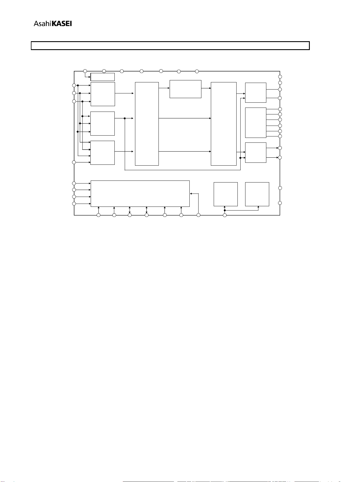
4. Block Diagram................................................................................................................................. 5
5. Pin Configurations and Functions................................................................................................... 6
■Pin Configurations.............................................................................................................................. 6
■Pin Functions ..................................................................................................................................... 7
■Handling of Unused Pin..................................................................................................................... 9
6. Absolute Maximum Ratings.......................................................................................................... 10
7. Recommended Operating Conditions .......................................................................................... 11
8. Electrical Characteristics .............................................................................................................. 12
■Analog Characteristics..................................................................................................................... 12
■DSD Mode........................................................................................................................................ 14
■Sharp Roll-Off Filter Characteristics................................................................................................ 15
■Slow Roll-Off Filter Characteristics.................................................................................................. 17
■Short Delay Sharp Roll-Off Filter Characteristics............................................................................ 19
■Short Delay Slow Roll-Off Filter Characteristics.............................................................................. 21
■Low Dispersion Short Delay Filter Characteristics.......................................................................... 23
■DSD Filter Characteristics................................................................................................................ 25
■DC Characteristics........................................................................................................................... 25
■Switching Characteristics................................................................................................................. 26
■Timing Diagram................................................................................................................................ 30
9. Functional Descriptions................................................................................................................. 35
■D/A Conversion Mode (PCM Mode, DSD Mode, EXDF Mode) ...................................................... 37
■D/A Conversion Mode Switching Timing ......................................................................................... 38
■System Clock................................................................................................................................... 39
■Audio Interface Format .................................................................................................................... 45
■Digital Filter...................................................................................................................................... 55
■De-emphasis Filter (PCM) ............................................................................................................... 55
■Output Volume (PCM, DSD and EXDF Modes; Register Control Mode only)................................ 56
■Gain Adjustment Function (PCM, DSD and EXDF Modes; Register Control Mode only).............. 57
■Zero Detection (PCM, DSD and EXDF Modes; Register Control Mode only) ................................ 57
■LR Channel Output Signal Select, Phase Inversion Function (PCM, DSD and EXDF Modes)...... 59
■Sound Quality Adjustment Function (PCM, DSD, EXDF; Register Control Mode only)................. 59
■DSD Signal Full-Scale (FS) Detection............................................................................................. 60
■Automatic Mode Switching Function (PCM/EXDF ⇔DSD Mode; Register Control Mode only).... 63
■Soft Mute Operation (PCM, DSD, EXDF)........................................................................................ 71
■LDO.................................................................................................................................................. 72
■Shutdown Switch.............................................................................................................................. 72
■Analog Output Overcurrent Protection............................................................................................. 72
■Power Up/Down Function................................................................................................................ 73
■Power-OFF/Reset Function............................................................................................................. 77
■Synchronize Function (PCM, EXDF)............................................................................................... 80
■Register Control Interface................................................................................................................ 82
■Register Map.................................................................................................................................... 86
■Register Definitions.......................................................................................................................... 88
10. Recommended External Circuits.................................................................................................. 96
11. Package...................................................................................................................................... 101
■Outline Dimensions (48-pin LQFP)................................................................................................101
■Material & Terminal Finish.............................................................................................................101
■Marking...........................................................................................................................................102

[AK4493]
017012230-E-00 2017/12
- 4 -
12. Ordering Guide ...........................................................................................................................103
■Ordering Guide............................................................................................................................... 103
13. Revision History..........................................................................................................................103
IMPORTANT NOTICE............................................................................................................................104

[AK4493]
017012230-E-00 2017/12
- 5 -
4. Block Diagram
MCLK
SDATA/DSDL/DINL
SMUTE/CSN
BICK/DCLK/BCK
SD/CCLK/SCL
SLOW/CDTI/SDA
VSSR
VDDR
PDN
AVDD
SCF
SCF
Clock
Divider
DVSS
DVDD
SSLOW/WCK
ACKS/
CAD1
PSN
DIF0/
DZFL
DIF2/
CAD0
VSSL
VDDL
VCML
AOUTRN
VCMR
VREFHL
VREFLL
VREFLR
VREFHR
AVSS
AOUTLP
AOUTLN
AOUTRP
PCM
Data
Interface
External
DF
Interface
Control
Register
Bias
Vref
LRCK/DSDR/DINR
DEM0
DIF1/
DZFR
DATT
Soft Mute
Modulator
Volume bypass
DSDD bit “1”
Normal path
DSDD bit “0”
I2C/INV
LDO
LDOE
TVDD
De-emphasis
&
Interpolator
DSD Data
Interface
&
DSD Filter
MCLK
Stop
Detection
TESTE
Figure 1. Block Diagram

[AK4493]
017012230-E-00 2017/12
- 6 -
5. Pin Configurations and Functions
■Pin Configurations
37
36
38
39
40
41
42
43
44
45
46
47
35
34
33
32
31
30
29
28
27
26
DVDD
1
2
PDN
3
BICK/DCLK/BCK
4
5
6
7
8
9
10
11
23
22
21
20
19
18
17
16
15
14
13
Top View
48
12
24
25
AK4493
SDATA/DSDL/DINL
SMUTE/CSN
LRCK/DSDR/DINR
SSLOW/WCK
SD/CCLK/SCL
SLOW/CDTI/SDA
DIF0/DZFL
DIF1/DZFR
DEM0
LDOE
INV/I2C
PSN
VREFHR
VREFHR
OUTRP
VREFLR
VREFLR
NC
VCMR
ACKS/CAD1
AOUTLN
VDDL
VDDL
VSSL
VSSL
VSSR
VSSR
VDDR
VDDR
AOUTRN
AOUTRP
VCML
VREFLL
VREFLL
VREFHL
VREFHL
AVSS
MCLK
DVSS
TVDD
AVDD
1
NC
AOUTLP
NC
1
DIF2/CAD0
TESTE
Figure 2. Pin Layout

[AK4493]
017012230-E-00 2017/12
- 7 -
■Pin Functions
No.
Pin Name
I/O
Function
1
DVDD
O
(LDOE pin = “H”)
LDO OutputPin, This pin should be connected to DVSS with 1.0µF (+/-50%).
This pin is prohibited to connect other devices.
-
(LDOE pin = “L”)
1.8V Power Input Pin
2
PDN
I
Power-Down Mode Pin
When at “L”, the AK4493 is in power-down mode and is held in reset.
The AK4493 must always be reset upon power-up.
3
BICK
I
Audio Serial Data Clock Pin in PCM Mode
DCLK
I
DSD Clock Pin in DSD Mode
BCK
I
Audio Serial Data Clock Pin in EXDF Mode
4
SDATA
I
Audio Serial Data Input Pin in PCM Mode
DSDL
I
DSD Lch Data Input Pin in DSD Mode
DINL
I
Lch Audio Serial Data Input Pin in EXDF Mode
5
LRCK
I
L/R Clock Pin in PCM Mode
DSDR
I
DSD Rch Data Input Pin in DSD Mode
DINR
I
Rch Audio Serial Data Input Pin in EXDF Mode
6
SSLOW
I
Digital filter setting in Pin Control Mode
WCK
I
Word Clock input pin in EXDF Mode
7
SMUTE
I
Soft Mute Pin in Pin Control Mode
When this pin is changed to “H”, soft mute cycle is initiated.
When returning “L”, the output mute releases.
CSN
I
Chip Select Pin in Register Control Mode, I2C = “L”
8
SD
I
Digital filter setting in Pin Control Mode
CCLK
I
Control Data Clock Pin in Register Control Mode, I2C = “L”
SCL
I
Control Data Clock Pin in Register Control Mode, I2C = “H”
9
SLOW
I
Digital filter setting in Pin Control Mode
CDTI
I
Control Data Input Pin in Register Control Mode, I2C = “L”
SDA
I/O
Control Data Clock Pin in Register Control Mode, I2C = “H”
10
DIF0
I
Digital Input Format 0 Pin in PCM Mode
DZFL
O
Lch Zero Input Detect Pin in Serial Control Mode (Internal pull-down pin)
11
DIF1
I
Digital Input Format 1 Pin in PCM Mode
DZFR
O
Rch Zero Input Detect Pin in Register Control Mode (Internal pull-down pin)
12
DIF2
I
Digital Input Format 2 Pin in PCM Mode
CAD0
I
Chip Address 0 Pin in Register Control Mode
13
PSN
I
Pin or Register Control mode Select Pin (Internal pull-up pin)
“L”: Register Control Mode, “H”: Pin Control Mode
14
INV
I
L/R channel Output Polarity Select Pin in Pin Control Mode
I2C
I
I2C mode select pin in Register Control Mode
15
DEM0
I
44.1k De-emphasis Enable Pin in Pin Control Mode. “L”: Enable, “H”: Disable
16
LDOE
I
Internal LDO Enable Pin. “L”: Disable, “H”: Enable

[AK4493]
017012230-E-00 2017/12
- 8 -
No.
Pin Name
I/O
Function
17
ACKS
I
Master Clock Auto Setting Mode Pin in Pin Mode
“L”: Manual Setting Mode, “H”: Auto Setting Mode
CAD1
I
Chip Address 1 Pin in Serial Control Mode
18
TESTE
I
Test Mode Enable pin. (Internal pull-down pin)
19
VREFHR
I
Rch High Level Voltage Reference Input Pin
20
VREFHR
I
Rch High Level Voltage Reference Input Pin
21
VREFLR
I
Rch Low Level Voltage Reference Input Pin
21
VREFLR
I
Rch Low Level Voltage Reference Input Pin
23
VCMR
-
Right channel Common Voltage Pin,
Connect this pin to VREFLR with a 10uF electrolytic capacitor.
This pin is prohibited to connect to any other load.
24
NC
-
No internal bonding.
Connect to GND.
25
AOUTRP
O
Rch Positive Analog Output Pin
26
AOUTRN
O
Rch Negative Analog Output Pin
27
VDDR
-
Rch Analog Power Supply Pin, 4.75 5.25V
28
VDDR
-
Rch Analog Power Supply Pin, 4.75 5.25V
29
VSSR
Ground Pin
30
VSSR
Ground Pin
31
VSSL
Ground Pin
32
VSSL
Ground Pin
33
VDDL
-
Lch Analog Power Supply Pin, 4.75 5.25V
34
VDDL
-
Lch Analog Power Supply Pin, 4.75 5.25V
35
AOUTLN
O
Lch Negative Analog Output Pin
36
AOUTLP
O
Lch Positive Analog Output Pin
37
NC
-
No internal bonding.
Connect to GND.
38
VCML
-
Left channel Common Voltage Pin,
Connect this pin to VREFLL with a 10uF electrolytic capacitor.
This pin is prohibited to connect to any other load.
39
VREFLL
I
Lch Low Level Voltage Reference Input Pin
40
VREFLL
I
Lch Low Level Voltage Reference Input Pin
41
VREFHL
I
Lch High Level Voltage Reference Input Pin
42
VREFHL
I
Lch High Level Voltage Reference Input Pin
43
NC
-
No internal bonding.
Connect to GND.
44
AVDD
-
Analog Power Supply Pin,
(LDOE pin = “H”) AVDD = 3.0 3.6V, (LDOE pin = “L”) AVDD = DVDD 3.6V
45
AVSS
-
Ground Pin
46
MCLK
I
Master Clock Input Pin
47
DVSS
-
Ground Pin
48
TVDD
-
Digital Power Supply Pin,
(LDOE pin = “H”) TVDD = 3.0 3.6V, (LDOE pin = “L”) TVDD = DVDD 3.6V
Note 1. All input pins except internal pull-up/down pins must not be left floating.
Note 2. The AK4493 must be reset by the PDN pin when changing control mode (Pin Control ⇔Register
Control) by the PSN pin.
Note 3. PCM mode, DSD mode and EXDF mode are controlled by register settings.

[AK4493]
017012230-E-00 2017/12
- 9 -
■Handling of Unused Pin
Unused I/O pins must be connected appropriately.
(1) Pin Control Mode (PCM mode only)
Classification
Pin Name
Status
Analog
AOUTLP, AOUTLN
Open
AOUTRP, AOUTRN
Open
Digital
TESTE
Connect to DVSS
or Open
(2) Register Control Mode
1. PCM Mode
Classification
Pin Name
Status
Analog
AOUTLP, AOUTLN
Open
AOUTRP, AOUTRN
Open
Digital
WCK, DEM0
Connect to DVSS
TESTE
Connect to DVSS
or Open
DZFL, DZFR
Open
2. DSD Mode
Classification
Pin Name
Status
Analog
AOUTLP, AOUTLN
Open
AOUTRP, AOUTRN
Open
Digital
WCK, DEM0
Connect to DVSS
TESTE
Connect to DVSS
or Open
DZFL, DZFR
Open
3. EXDF Mode
Classification
Pin Name
Status
Analog
AOUTLP, AOUTLN
Open
AOUTRP, AOUTRN
Open
Digital
DEM
Connect to DVSS
TESTE
Connect to DVSS
or Open
DZFL, DZFR
Open
4. With I2C-Bus
Classification
Pin Name
Status
Digital
CSN
Connect to DVSS

[AK4493]
017012230-E-00 2017/12
- 10 -
5. Pull-up, Pull-down Pin List
Classification
Pin Name
Internal connection
pull-up pin (typ = 100kΩ)
PSN
TVSS
pull-down pin(typ = 100kΩ)
DZFL, DZFR, TESTE
DVSS
6. Absolute Maximum Ratings
(AVSS = DVSS = VSSL = VSSR = VREFLL = VREFLR = 0V;Note 4)
Parameter
Symbol
Min.
Max.
Unit
Power
Supplies:
Digital I/O
Digital Core
Clock Interface
Analog
|AVSS DVSS| (Note 5)
|AVSS VSSL| (Note 5)
|AVSS VSSR| (Note 5)
|DVSS VSSL| (Note 5)
|DVSS VSSR| (Note 5)
|VSSL VSSR| (Note 5)
TVDD
DVDD
AVDD
VDDL/R
GND
GND
GND
GND
GND
GND
0.3
0.3
0.3
0.3
-
-
-
-
-
-
4.0
2.5
4.0
6.0
0.3
0.3
0.3
0.3
0.3
0.3
V
V
V
V
V
V
V
V
V
V
Voltage
Reference
“H”voltage reference
(Note 6)
“L”voltage reference
VREFHL/R
VREFLL/R
-0.3
-0.3
VDDL/R+0.3
Or 6.0
+0.3
V
V
Input Current, Any Pin Except Supplies
IIN
-
10
mA
Digital Input Voltage
(Note 7)
VIND
0.3
TVDD+0.3
or 4.0
V
Ambient Temperature (Power supplied)
Ta
40
85
C
Storage Temperature
Tstg
65
150
C
Note 4. All voltages with respect to ground.
Note 5. AVSS, DVSS, VSSL and VSSR must be connected to the same analog ground plane.
Note 6. Regarding VREFHL/R pins, maximum value which is lower value (VDDL/R+0.3) or 6.0V.
Note 7. Regarding Digital input pins, maximum value which is lower value (VDDL/R+0.3) or 4.0V.
WARNING: Operation at or beyond these limits may result in permanent damage to the device.
Normal operation is not guaranteed at these extremes.

[AK4493]
017012230-E-00 2017/12
- 11 -
7. Recommended Operating Conditions
(AVSS = DVSS = VSSL = VSSR = VREFLL = VREFLR = 0V;Note 4)
Parameter
Symbol
Min.
Typ.
Max.
Unit
Power Supplies
(Note 8)
■LDOE pin = “L”
Digital I/O
Clock Interface
Digital Core
Analog
■LDOE pin = “H”
Digital I/O
Clock Interface
Analog
TVDD
AVDD
DVDD
VDDL/R
TVDD
AVDD
VDDL/R
DVDD
DVDD
1.7
4.75
3.0
3.0
4.75
1.8
1.8
1.8
5.0
3.3
3.3
5.0
3.6
3.6
1.98
5.25
3.6
3.6
5.25
V
V
V
V
V
V
V
Voltage Reference
(Note 8)
“H” voltage reference
“L” voltage reference
VREFHL/R
VREFLL/R
VDDL/R-0.5
-
-
VSSL/R
VDDL/R
-
V
V
Note 4. All voltages with respect to ground.
Note 8.The analog output voltage scales with the voltage of (VREFHL/R VREFLL/R).
Note 9.TVDD must be powered up before AVDD or at the same time. When not using the internal LDO
(LDOE pin = “L”), TVDD must be powered up before DVDD or at the same time.
Note 10. The internal LDO outputs DVDD (1.8V) when the LDOE pin = “H”.
* AKM assumes no responsibility for the usage beyond the conditions in this data sheet.

[AK4493]
017012230-E-00 2017/12
- 12 -
8. Electrical Characteristics
■Analog Characteristics
(Ta = 25C; LDOE pin = “L”, AVDD = TVDD = 3.3V, DVDD = 1.8V; AVSS = DVSS = VSSL/R = 0V;
VREFHL/R = VDDL/R = 5.0V, VREFLL/R = 0V; Input data = 24bit; BICK = 64fs; Signal Frequency= 1kHz;
Sampling Frequency = 44.1kHz; Measurement bandwidth = 20Hz ~ 20kHz; External Circuit: Example
Circuit 3 (Figure 81); SC[1:0] bits = “00”; 2Vrms output mode (GC[2:0] bits = “000”); unless otherwise
specified.)
Parameter
Min.
Typ.
Max.
Unit
Resolution
-
-
32
Bit
Dynamic Characteristics (Note 11)
THD+N
fs=44.1kHz
BW=20kHz
0dBFS
GC[2:0]=“000”
-
-113
-105
dB
GC[2:0]=“100”
-
-110
-
60dBFS
-
-60
-
dB
fs=96kHz
BW=40kHz
0dBFS
-
-110
-
dB
60dBFS
-
-57
-
dB
fs=192kHz
BW=40kHz
0dBFS
-
-107
-
dB
60dBFS
-
-57
-
dB
BW=80kHz
60dBFS
-
-54
-
dB
fs=384kHz
BW=40kHz
0dBFS
-
-107
-
dB
fs=768kHz
BW=40kHz
0dBFS
-
-107
-
dB
Dynamic Range (60dBFS with A-weighted) (Note 12)
118
123
-
dB
S/N (A-weighted) (Note 13)
GC[2:0] = “000”
118
123
-
dB
GC[2:0] = “100”
Stereo mode
120
125
-
dB
Mono mode
(Note 17)
-
126
-
Inter-channel Isolation
110
120
-
dB
DC Accuracy
Inter-channel Gain Mismatch
-
0.15
0.3
dB
Gain Drift
-
20
-
ppm/C
Output
Voltage
GC[2:0] bits = “000”(Note 14)
2.65
2.8
2.95
Vpp
GC[2:0] bits = “100”(Note 15)
3.55
3.75
3.95
Vpp
Load Resistance (Note 16)
450
-
-
Load Capacitance (Note 16)
-
-
25
pF
Note 11. Measured by Audio Precision APx555. Averaging mode.
Note 12. 101dB at 16bit data and 118dB at 20bit data.
Note 13. S/N ratio does not depend on input bit length.
Note 14. The analog output voltage with 0dBFS input signal when GC[2:0] bits = “000”is calculated by
the following formula:
AOUTL/R (typ. @0dB) = (AOUT+) (AOUT) = 2.8Vpp (VREFHL/R VREFLL/R)/5.
This expression is equivalent to 5.6Vpp and is differential and irrespective of ground reference
or the Vcom bias voltage.
Note 15. The analog output voltage with 0dBFS inputsignal when GC[2:0] bits = “100”is calculated by the
following formula:
AOUTL/R (typ. @0dB) = (AOUT+) (AOUT) = 3.75Vpp (VREFHL/R VREFLL/R)/5.
This expression is equivalent to 7.5Vpp and is differential and irrespective of ground reference
or the Vcom bias voltage.
Note 16. The load resistance value is 450 ohm (Min) against the DC load (No DC cut capacitor) with
respect to ground. The load capacitance value with respect to ground. Analog characteristics
are sensitive to capacitive load that is connected to the output pin. Therefore, the capacitive load
must be minimized.
Note 17. When using the circuit shown in Figure 82

[AK4493]
017012230-E-00 2017/12
- 13 -
(Ta = 25C; AVDD = TVDD = 3.3V, DVDD = 1.8V (LDOE pin = “L”), AVSS = DVSS = VSSL/R = 0V;
VREFHL/R = VDDL/R = 5.0V, VREFLL/R = 0V; Input data = 24bit; BICK = 64fs; Signal Frequency= 1kHz;
Sampling Frequency = 44.1kHz; SC[1:0] bits = “00”; 2Vrms output mode (GC[2:0] bits = “000”); unless
otherwise specified.)
Power Supplies
Parameter
Min.
Typ.
Max.
Unit
Power Supply Current
Normal operation (PDN pin = “H”)
VDDL/R (total)
-
33
50
mA
VREFHL/R
-
1
1.5
mA
AVDD
-
1
1.5
mA
TVDD
LDOE pin = “H”
fs = 44.1kHz
-
9
13.5
mA
fs = 96kHz
-
15
22.5
mA
fs = 192kHz
-
23
34.5
mA
LDOE pin = “L”
-
1
1.5
mA
DVDD
LDOE pin = “L”
fs = 44.1kHz
-
8
12
mA
fs = 96kHz
-
14
21
mA
fs = 192kHz
-
22
33
mA
Total IDD (fs = 44.1kHz)
-
44
66.5
mA
Power down (PDN pin = “L”) (Note 18)
TVDD + AVDD + VDDL/R + DVDD
-
10
100
A
Note 18.In power down mode, the PSN pin = TVDD and all other digital input pins including clock pins
(MCLK, BICK and LRCK) are held to DVSS.
Note 19. The DVDD pin becomes an output pin when the LDOE pin = “H”.

[AK4493]
017012230-E-00 2017/12
- 14 -
■DSD Mode
(Ta = 25C; AVDD = TVDD = 3.3V, DVDD = 1.8V (LDOE pin = “L”), AVSS = DVSS = VSSL/R = 0V;
VREFHL/R = VDDL/R = 5.0V, VREFLL/R = 0V; Signal Frequency = 1kHz; Measurement bandwidth =
20Hz ~ 20kHz; External Circuit: Example Circuit 3 (Figure 81); SC[1:0] bits = “00”; 2Vrms output mode
(GC[2:0] bits = “000”); unless otherwise specified.)
Parameter
Min.
Typ.
Max.
Unit
Dynamic Characteristics
THD+N
(Note 20)
DSD Datastream: DSD64
0dBFS
-
-113
-
dB
DSD Datastream: DSD128
0dBFS
-
-113
-
dB
DSD Datastream: DSD256
0dBFS
-
-113
-
dB
S/N
(A-weighted,
Normal path)
(Note 20)
DSD Datastream: DSD64
Digital “0”
(Note 23)
-
123
-
dB
DSD Datastream: DSD128
Digital “0”
(Note 23)
-
123
-
dB
DSD Datastream: DSD256
Digital “0”
(Note 23)
-
123
-
dB
DC Accuracy
Output Voltage (Normal path) (Note 14)
2.65
2.8
2.95
Vpp
Output Voltage (Volume Bypass) (Note 24)
2.38
2.5
2.63
Vpp
Note 20. DSD Datastream: Analog characteristics are not guaranteed with DSD512 datastream.
Note 21. The peak level of DSD signal should be in the range of 25% ~ 75% duty according to the SACD
format book (Scarlet Book).
Note 22. The output level is assumed as 0dB when a 1kHz 25% ~ 75% duty sine wave is input. Click
noise may occur if the input signal exceeds 0dB.
Note 23. Digital “0” is a digital zero code pattern (“01101001”) according to the SACD format book
(Scarlet Book).
Note 24. When DSDD bit = “1”, the analog output voltage at 25% ~ 75% input signal duty is calculated by
the following equation:
AOUTL/R (typ. @0dB) = (AOUTLP/RP) (AOUTLN/RN)
= 2.8Vpp (VREFHL/R VREFLL/R)/5.0.
This expression is equivalent to 5.6Vpp and is differential and irrespective of ground reference
or the Vcom bias voltage.
Note 25. When DSDD bit = “1”, the analog output voltage at 25% ~ 75% input signal duty is calculated by
the following equation:
AOUTL/R (typ. @0dB) = (AOUTLP/RP) (AOUTLN/RN)
= 2.5Vpp (VREFHL/R VREFLL/R)/5.0.
This expression is equivalent to 5.0Vpp and is differential and irrespective of ground reference
or the Vcom bias voltage.

[AK4493]
017012230-E-00 2017/12
- 15 -
■Sharp Roll-Off Filter Characteristics
Sharp Roll-Off Filter Characteristics (fs = 44.1kHz)
(Ta = -40 ~ 85C; VDDL/R = 4.75 5.25V, AVDD = TVDD = 1.7 3.6V, DVDD = 1.7~ 1.98V;
Normal Speed Mode;DEM = OFF; SD bit= “0” or SD pin = “L”, SLOW bit =“0” or SLOW pin = “L”,SSLOW
bit = “0” or SSLOW pin = “L”)
Parameter
Symbol
Min.
Typ.
Max.
Unit
Digital Filter
Frequency Response
(Note 26)
0.01dB
6.0dB
-
-
0
-
22.05
20.0
-
kHz
kHz
Passband (Note 27)
PB
0
20.0
kHz
Stopband (Note 27)
SB
24.1
kHz
Passband Ripple (Note 28)
PR
0.005
dB
Stopband Attenuation (Note 26)
SA
100
dB
Group Delay (Note
296)
GD
-
29.2
-
1/fs
Digital Filter + SCF (Note 26)
Frequency Response: 0 20.0kHz
-
-0.2
-
+0.1
dB
Sharp Roll-Off Filter Characteristics (fs = 96kHz)
(Ta = -40 ~ 85C; VDDL/R = 4.75 5.25V, AVDD = TVDD = 1.7 3.6V, DVDD = 1.7 ~ 1.98V;
Double Speed Mode; DEM = OFF; SD bit = “0” or SD pin = “L”, SLOW bit = “0” or SLOW pin = “L”,SSLOW
bit = “0” or SSLOW pin = “L”)
Parameter
Symbol
Min.
Typ.
Max.
Unit
Digital Filter
Frequency Response
(Note 26)
0.01dB
6.0dB
-
-
0
-
48.0
43.5
-
kHz
kHz
Passband (Note 27)
PB
0
43.5
kHz
Stopband (Note 27)
SB
52.5
kHz
Passband Ripple (Note 28)
PR
0.005
dB
Stopband Attenuation (Note 26)
SA
100
dB
Group Delay (Note
296)
GD
-
29.2
-
1/fs
Digital Filter + SCF (Note 26)
Frequency Response: 0 40.0kHz
-0.6
-
+0.1
dB
Sharp Roll-Off Filter Characteristics (fs = 192kHz)
(Ta = -40 ~ 85C; VDDL/R = 4.75 5.25V, AVDD = TVDD = 1.7 3.6V, DVDD = 1.7 ~ 1.98V;
Quad Speed Mode; DEM = OFF; SD bit = “0” or SD pin = “L”, SLOW bit = “0” or SLOW pin = “L”, SSLOW
bit = “0” or SSLOW pin = “L”)
Parameter
Symbol
Min.
Typ.
Max.
Unit
Digital Filter
Frequency Response
(Note 26)
0.01dB
6.0dB
-
-
0
-
96.0
87.0
-
kHz
kHz
Passband (Note 27)
PB
0
87.0
kHz
Stopband (Note 27)
SB
104.9
kHz
Passband Ripple (Note 28)
PR
0.005
dB
Stopband Attenuation (Note 26)
SA
100
dB
Group Delay (Note
296)
GD
-
29.2
-
1/fs
Digital Filter + SCF (Note 26)
Frequency Response: 0 80.0kHz
-2.0
-
+0.1
dB
Note 26. Frequency response refers to the output level (0dB) of a 1kHz, 0dB sine wave input. Stopband
attenuation band ranges from SB to 4fs.

[AK4493]
017012230-E-00 2017/12
- 16 -
Note 27. The passband and stopband frequencies scale with fs. For example, PB = 0.4535×fs
(@0.01dB), SB = 0.546×fs.
Note 28. This value is the gain amplitude of first step interpolator which is 4 times oversampling filter in
pass band width.
Note 29. The calculating delay time which occurred by digital filtering. This time is from setting the
16/20/24/32 bit data of both channels to the output of analog signal.
Figure 3. Sharp Roll-off Filter Frequency Response
Figure 4. Sharp Roll-off Filter Passband Ripple

[AK4493]
017012230-E-00 2017/12
- 17 -
■Slow Roll-Off Filter Characteristics
Slow Roll-Off Filter Characteristics (fs = 44.1kHz)
(Ta = -40~85C; VDDL/R = 4.755.25V, AVDD = TVDD = 1.7~3.6V, DVDD = 1.7~1.98V; Normal Speed
Mode; DEM = OFF; SD bit = “0” or SD pin = “L”, SLOW bit = “1”or SLOW pin = “H”, SSLOW bit = “0” or
SSLOW pin = “L”)
Parameter
Symbol
Min.
Typ.
Max.
Unit
Digital Filter
Frequency Response
(Note 26)
0.01dB
6.0dB
-
-
0
-
-
21.0
8.0
-
kHz
kHz
Passband (Note 30)
PB
0
-
8.0
kHz
Stopband (Note 30)
SB
39.2
-
-
kHz
Passband Ripple (Note 28)
PR
-
-
0.007
dB
Stopband Attenuation (Note 26)
SA
92
-
-
dB
Group Delay (Note 29)
GD
-
6.5
-
1/fs
Digital Filter + SCF (Note 26)
Frequency Response: 0 20.0kHz
-5.0
-
+0.1
dB
Slow Roll-Off Filter Characteristics (fs = 96kHz)
(Ta = -40~85C; VDDL/R = 4.75 5.25V, AVDD = TVDD = 1.73.6V, DVDD = 1.7~1.98V; Double Speed
Mode; DEM = OFF; SD bit = “0” or SD pin = “L”, SLOW bit = “1”or SLOW pin = “H”, SSLOW bit = “0” or
SSLOW pin = “L”)
Parameter
Symbol
Min.
Typ.
Max.
Unit
Digital Filter
Frequency Response
(Note 26)
0.01dB
6.0dB
-
-
0
-
-
45.6
17.6
-
kHz
kHz
Passband (Note 30)
PB
0
-
17.6
kHz
Stopband (Note 30)
SB
85.4
-
-
kHz
Passband Ripple (Note 28)
PR
-
-
0.007
dB
Stopband Attenuation (Note 26)
SA
92
-
-
dB
Group Delay (Note 29)
GD
-
6.5
-
1/fs
Digital Filter + SCF (Note 26)
Frequency Response: 0 40.0kHz
-3.8
-
+0.1
dB
Slow Roll-Off Filter Characteristics (fs = 192kHz)
(Ta = -40 ~ 85C; VDDL/R = 4.75 5.25V, AVDD = TVDD = 1.7 3.6V, DVDD = 1.7 ~ 1.98V;
Quad Speed Mode; DEM = OFF; SD bit = “0” or SD pin = “L”, SLOW bit = “1”or SLOW pin = “H”, SSLOW
bit = “0” or SSLOW pin = “L”)
Parameter
Symbol
Min.
Typ.
Max.
Unit
Digital Filter
Frequency Response
(Note 26)
0.01dB
6.0dB
-
-
0
-
-
91.2
35.2
-
kHz
kHz
Passband (Note 30)
PB
0
-
35.2
kHz
Stopband (Note 30)
SB
170.7
-
-
kHz
Passband Ripple (Note 28)
PR
-
-
0.007
dB
Stopband Attenuation (Note 26)
SA
100
-
-
dB
Group Delay (Note 29)
GD
-
6.5
-
1/fs
Digital Filter + SCF (Note 26)
Frequency Response: 0 80.0kHz
-5.0
-
+0.1
dB
Note 307. The passband and stopband frequencies scale with fs.
For example, PB = 0.1836 fs (@0.01dB), SB = 0.8889 fs.

[AK4493]
017012230-E-00 2017/12
- 18 -
Figure 5. Slow Roll-off Filter Frequency Response
Figure 6. Slow Roll-off Filter Passband Ripple

[AK4493]
017012230-E-00 2017/12
- 19 -
■Short Delay Sharp Roll-Off Filter Characteristics
Short Delay Sharp Roll-Off Filter Characteristics (fs = 44.1kHz)
(Ta = -40 ~ 85C; VDDL/R = 4.75 5.25V, AVDD = TVDD = 1.7 3.6V, DVDD = 1.7 ~ 1.98V;
Normal Speed Mode; DEM = OFF; SD bit = “1”or SD pin = “H”, SLOW bit = “0”or SLOW pin = “L”,
SSLOW bit = “0” or SSLOW pin = “L”)
Parameter
Symbol
Min.
Typ.
Max.
Unit
Digital Filter
Frequency Response
(Note 26)
0.01dB
6.0dB
-
-
0
-
-
22.05
20.0
-
kHz
kHz
Passband (Note 31)
PB
0
-
20.0
kHz
Stopband (Note 31)
SB
24.1
-
-
kHz
Passband Ripple (Note 28)
PR
-
-
0.005
dB
Stopband Attenuation (Note 26)
SA
100
-
-
dB
Group Delay (Note 29)
GD
-
6.0
-
1/fs
Digital Filter + SCF (Note 26)
Frequency Response: 0 20.0kHz
-0.2
-
+0.1
dB
Short Delay Sharp Roll-Off Filter Characteristics (fs = 96kHz)
(Ta = -40 ~ 85C; VDDL/R = 4.75 5.25V, AVDD = TVDD = 1.7 3.6V, DVDD = 1.7 ~ 1.98V;
Double Speed Mode; DEM = OFF; SD bit = “1”or SD pin = “H”, SLOW bit = “0”or SLOW pin = “L”,
SSLOW bit = “0” or SSLOW pin = “L”)
Parameter
Symbol
Min.
Typ.
Max.
Unit
Digital Filter
Frequency Response
(Note 26)
0.01dB
6.0dB
-
-
0
-
-
48.0
43.5
-
kHz
kHz
Passband (Note 31)
PB
0
-
43.5
kHz
Stopband (Note 31)
SB
52.5
-
-
kHz
Passband Ripple (Note 28)
PR
-
-
0.005
dB
Stopband Attenuation (Note 26)
SA
100
-
-
dB
Group Delay (Note 29)
GD
-
6.0
-
1/fs
Digital Filter + SCF (Note 26)
Frequency Response: 0 40.0kHz
-0.6
-
+0.1
dB
Short Delay Sharp Roll-Off Filter Characteristics (fs = 192kHz)
(Ta = -40 ~ 85C; VDDL/R = 4.75 5.25V, AVDD = TVDD = 1.7 3.6V, DVDD = 1.7 ~ 1.98V;
Quad Speed Mode; DEM = OFF; SD bit = “1”or SD pin = “H”, SLOW bit = “0”or SLOW pin = “L”, SSLOW
bit = “0” or SSLOW pin = “L”)
Parameter
Symbol
Min.
Typ.
Max.
Unit
Digital Filter
Frequency Response
(Note 26)
0.01dB
6.0dB
-
-
0
-
-
96.0
87.0
-
kHz
kHz
Passband (Note 31)
PB
0
-
87.0
kHz
Stopband (Note 31)
SB
104.9
-
-
kHz
Passband Ripple (Note 28)
PR
-
-
0.005
dB
Stopband Attenuation (Note 26)
SA
100
-
-
dB
Group Delay (Note 29)
GD
-
6.0
-
1/fs
Digital Filter + SCF (Note 26)
Frequency Response: 0 80.0kHz
-2.0
-
+0.1
dB
Note 318. The passband and stopband frequencies scale with fs.
For example, PB = 0.4535 fs (@0.01dB), SB = 0.546 fs.

[AK4493]
017012230-E-00 2017/12
- 20 -
Figure 7. Short Delay Sharp Roll-off Filter Frequency Response
Figure 8. Short Delay Sharp Roll-off Filter Passband Ripple
Table of contents
Other Asahi KASEI Measuring Instrument manuals
Popular Measuring Instrument manuals by other brands

PCB Piezotronics
PCB Piezotronics 3741F122G Installation and operating manual

Special Pie
Special Pie J10C user manual

HEIDENHAIN
HEIDENHAIN ECN 1324 S Mounting instructions

Tecson
Tecson e-litro Series START-UP & OPERATION

PCI
PCI OAFE-2000 Installation, operation & maintenance manual

Bosch
Bosch UniversalDistance 30 Original instructions