Asus P/I-P55T2P4 User manual

R
P/I-P55T2P4
Pentium Motherboard
USER'S MANUAL

ASUS P/I-P55T2P4 User's Manual
II
USER'S NOTICE
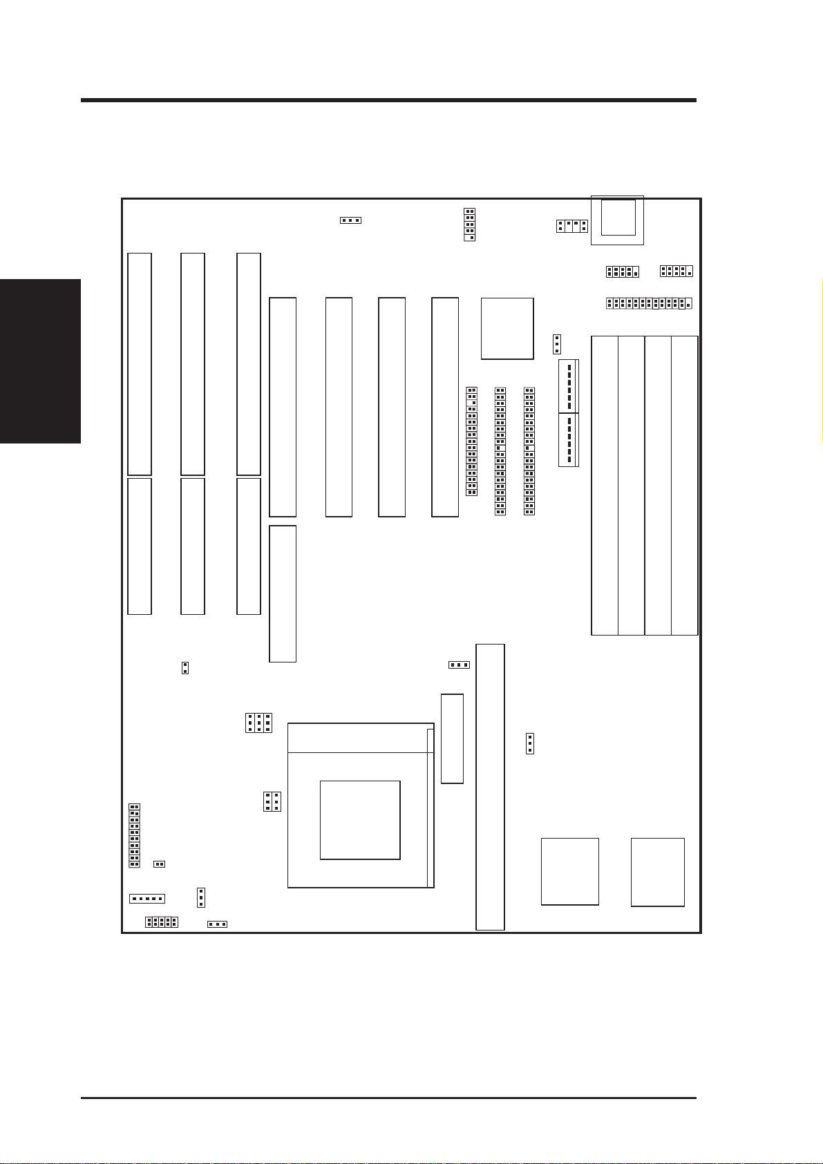
Product Name: ASUS P/I-P55T2P4
Manual Revision: 3.11
Release Date: May 1997
No part of this product, including the product and software may be reproduced,
transmitted, transcribed, stored in a retrieval system, or translated into any lan-
guageinanyformbyanymeanswithouttheexpresswrittenpermissionofASUSTeK
COMPUTER INC. (hereinafter referred to as ASUS) except documentation kept
by the purchaser for backup purposes.
Specifications are subject to change without notice. ASUS provides this manual
“as is” without warranty of any kind, either express or implied, including but not
limited to the implied warranties or conditions of merchantability or fitness for a
particular purpose. In no event shallASUS be liable for any loss or profits, loss of
business, loss of use or data, interruption of business, or for indirect, special, inci-
dental, or consequential damages of any kind, even if ASUS has been advised of
the possibility of such damages arising from any defect or error in this manual or
product. ASUS may revise this manual from time to time without notice.
Products mentioned in this manual are mentioned for identification purposes only.
Product names appearing in this manual may or may not be registered trademarks
or copyrights of their respective companies.
• Intel, LANDesk, and Pentium are registered trademarks of Intel Corporation.
• IBM is a registered trademark of International Business Machines Corp.
• Symbios is a registered trademark of Symbios Logic Corporation.
• Windows and MS-DOS are registered trademarks of Microsoft Corporation.
• Sound Blaster AWE32 and SB16 are trademarks of Creative Technology Ltd.
• Adobe andAcrobat are registered trademarks of Adobe Systems Incorporated.
The product name and revision number are both printed on the board itself. Manual
revisions are released for each board design represented by the digit before and
after the period of the manual revision number. Manual updates are represented by
the third digit in the manual revision number. For previous or updated manuals,
BIOS, drivers, or product release information you may visit the ASUS home page
at http://www.asus.com.tw/ or contact ASUS from the following page.
© Copyright 1997 ASUSTeK COMPUTER INC. All rights reserved.

ASUS P/I-P55T2P4 User's Manual III
ASUS CONTACT INFORMATION
ASUSTeK COMPUTER INC.
Marketing Info:
Address: 150 Li-Te Road, Peitou, Taipei, Taiwan, ROC
Telephone: 886-2-894-3447
Fax: 886-2-894-3449
Email: [email protected]
Technical Support:
Fax: 886-2-895-9254
BBS: 886-2-896-4667
Email: [email protected]
WWW: http://www.asus.com.tw/
Gopher: gopher.asus.com.tw
FTP: ftp.asus.com.tw/pub/ASUS
ASUS COMPUTER INTERNATIONAL
Marketing Info:
Address: 721 Charcot Avenue, San Jose, CA 95131, USA
Telephone: 1-408-474-0567
Fax: 1-408-474-0568
Email: [email protected]
Technical Support:
BBS: 1-408-474-0555
Email: [email protected]
ASUS COMPUTER GmbH
Marketing Info:
Address: Harkort Str. 25, 40880 Ratingen, BRD, Germany
Telephone: 49-2102-445011
Fax: 49-2102-442066
Email: [email protected]
Technical Support:
BBS: 49-2102-448690
Email: [email protected]

ASUS P/I-P55T2P4 User's Manual
IV
CONTENTS
I. INTRODUCTION......................................................... 1
How this manual is organized .......................................................... 1
Item Checklist .................................................................................. 1
II. FEATURES .................................................................. 2
Features of the ASUS Motherboard ................................................. 2
Parts of the ASUS Motherboard ...................................................... 3
III. INSTALLATION ........................................................ 4
Map of the Motherboard .................................................................. 4
Installation Steps .............................................................................. 6
1. Jumpers ........................................................................................ 6
Jumper Settings .................................................................... 7
Cyrix CPU Identification ...................................................... 11
2. System Memory (DRAM & SRAM) .......................................... 12
TAG SRAM Upgrade: .......................................................... 12
DRAM Memory Installation Procedures: ............................ 13
Static RAM (SRAM) for Level 2 (External) Cache ................... 14
Compatible Cache Modules for this Motherboard ............... 14
3. Central Processing Unit (CPU) ................................................... 15
4. Expansion Cards ......................................................................... 16
Expansion Card Installation Procedure: ............................... 16
Assigning IRQs for Expansion Cards................................... 16
Assigning DMA Channels for ISA Cards ............................. 17
ASUS MediaBus Card .......................................................... 18
5. External Connectors .................................................................... 19
Power Connection Procedures ................................................... 25
IV. BIOS SOFTWARE ..................................................... 26
Support Software ............................................................................. 26
Flash Memory Writer Utility ........................................................... 26
Main Menu ........................................................................... 26
Advanced Features Menu ..................................................... 27
Updating your Motherboard's BIOS .......................................... 28
6. BIOS Setup ................................................................................. 29
Load Defaults ....................................................................... 30
Standard CMOS Setup ............................................................... 30

ASUS P/I-P55T2P4 User's Manual V
CONTENTS
Details of Standard CMOS Setup: ........................................ 31
BIOS Features Setup .................................................................. 34
Details of BIOS Features Setup:........................................... 34
Chipset Features Setup ............................................................... 37
Power Management Setup.......................................................... 40
Details of Power Management Setup: .................................. 40
PNP and PCI Setup .................................................................... 42
Load BIOS Defaults ................................................................... 44
Load Setup Defaults ................................................................... 44
Supervisor Password and User Password .................................. 45
IDE HDD Auto Detection .......................................................... 46
Save and Exit Setup ................................................................... 47
Exit Without Saving ................................................................... 47
V. DESKTOP MANAGEMENT ...................................... 49
Desktop Management Interface (DMI) ............................................ 49
Introducing the ASUS DMI Configuration Utility ............... 49
System Requirements ........................................................... 49
Using the ASUS DMI Configuration Utility ........................ 50
Notes: .................................................................................... 50
VI. ASUS PCI-SC200 SCSI Card.................................... 53
NCR SCSI BIOS and Drivers .......................................................... 53
The ASUS PCI-SC200 SCSI Interface Card ................................... 54
Setting Up the ASUS PCI-SC200 .............................................. 54
Setting the INT Assignment ....................................................... 55
Terminator Settings .................................................................... 55
SCSI ID Numbers ...................................................................... 56
VII. ASUS I-A16C Audio Card ....................................... 57
ASUS I-A16C Audio Features ................................................... 57
Unpacking and Handling Precautions ........................................ 57
Layout and Connectors .............................................................. 58
Connectors ............................................................................ 58
CD-Audio Connector Pin Definitions ........................................ 58
VIII. DOS 3.1 & Windows 3.1x Audio Software
(with optional ASUS I-A16C Audio Card Bundle Only)
IX. Windows 95 Audio Software
(with optional ASUS I-A16C Audio Card Bundle Only)

ASUS P/I-P55T2P4 User's Manual
VI
FCC & DOC COMPLIANCE
FederalCommunicationsCommission Statement
This device complies with FCC Rules Part 15. Operation is subject to the following
two conditions:
• This device may not cause harmful interference, and
• This device must accept any interference received, including interference that
may cause undesired operation.
This equipment has been tested and found to comply with the limits for a Class B
digital device, pursuant to Part 15 of the FCC Rules. These limits are designed to
provide reasonable protection against harmful interference in a residential installa-
tion. This equipment generates, uses and can radiate radio frequency energy and, if
not installed and used in accordance with manufacturer's instructions, may cause
harmful interference to radio communications. However, there is no guarantee that
interference will not occur in a particular installation. If this equipment does cause
harmful interference to radio or television reception, which can be determined by
turning the equipment off and on, the user is encouraged to try to correct the inter-
ference by one or more of the following measures:
• Re-orient or relocate the receiving antenna.
• Increase the separation between the equipment and receiver.
• Connect the equipment to an outlet on a circuit different from that to which
the receiver is connected.
• Consult the dealer or an experienced radio/TV technician for help.
WARNING: Theuseofshieldedcablesforconnectionofthemonitortothegraphics
card is required to assure compliance with FCC regulations. Changes or modifica-
tions to this unit not expressly approved by the party responsible for compliance
could void the user's authority to operate this equipment.
CanadianDepartmentof Communications Statement
This digital apparatus does not exceed the Class B limits for radio noise emissions
from digital apparatus set out in the Radio Interference Regulations of the Cana-
dian Department of Communications.

ASUS P/I-P55T2P4 User’s Manual 1
I. INTRODUCTION
I. INTRODUCTION
(Manual / Checklist)
How this manual is organized
This manual is divided into the following sections:
I. Introduction: Manual information and checklist
II. Features: Information and specifications concerning this product
III. Installation: Instructions on setting up the motherboard.
IV. BIOS Setup: BIOS software setup information.
V. Software: Information on the included support software
VI. ASUS SCSI: Installation of an optional ASUS SCSI cards
VII. ASUS I-A16C: Installation of an optional 16-bit Audio card
VIII. DOS/Win3.1x: Audio Software Manual (with ASUS I-A16C bundle)
IX. Windows 95: Audio Software Manual (with ASUS I-A16C bundle)
Item Checklist
Please check that your package is complete. If you discover damaged or missing
items, please contact your retailer.
þThe ASUS P/I-P55T2P4 motherboard
þ2 serial port ribbon cables attached to a mounting bracket
þ1 parallel ribbon cable with mounting bracket
þ1 IDE ribbon cable
þ1 floppy ribbon cable
þSupport drivers and utilities as follows:
• Flash Memory Writer utility to update the FLASH BIOS
• Desktop Management Interface (DMI) utility
• Bus Master IDE Drivers for various operating systems
• Audio drivers and utilities (included withASUS I-A16C audio bundle only)
• Readme files for descriptions and use of the files
• Technical Support Form
þThis user's manual (Audio sections included withASUS I-A16C audio bundle)
¨Optional infrared module
¨Optional ASUS PCI-SC200 Fast-SCSI or PCI-SC860 Ultra-Fast SCSI card
¨Optional ASUS I-A16C audio card
¨Optional PS/2 mouse cable with mounting bracket
¨Optional ASUS pipelined burst cache module

2ASUS P/I-P55T2P4 User’s Manual
II. FEATURES
Features of the ASUS Motherboard
TheASUS P/I-P55T2P4 is carefully designed for the demanding PC user who wants
a great many features in a small package. This motherboard:
•Easy Installation: Is equipped with BIOS that supports auto detection of hard
drives and Plug and Play to make setup of hard drives and expansion cards
virtually automatic.
•VersatileProcessorSupport: IntelPentium
®
75-233MHz(P55C-MMX
™
,P54C/
P54CS), IBM
®
/Cyrix
®
6x86-PR166+ (Rev 2.7 or later), IBM
®
/Cyrix
®
6x86MX
™
(PR166 & above), AMD-K5
™
(PR75-PR133), AMD-K6
™
(PR166-PR233).
•Intel Chipset: Features Intel's 430HX PCIset with I/O subsystems.
•Error Checking and Correcting (ECC): Using Intel's 430HX PCIset together
with parity DRAM modules can detect multi-bit memory errors and correct 1-
bit memory errors.
•Desktop Management Interface (DMI): Supports DMI through BIOS which
allows hardware to communicate within a standard protocol creating a higher
level of compatibility (see section V).
•L2 Cache: Provides the option of 0KB upgradeable to 256KB or 512KB, on-
board256KB upgradeable to 512KB, or512KB onboard Pipelined Burst SRAM.
Upgrades are made through a Synchronous SRAM cache module. (See page
14 for compatible cache modules.)
•Versatile DRAM Memory Support: Supports 72-pin SIMMs of 4MB, 8MB,
16MB, 32MB, or 64MB to form a memory size between 8MB to 256MB. Sup-
ports both Fast Page Mode (FPM) and Extended Data Output (EDO) SIMMs.
•ISA and PCI Expansion Slots: Provides three 16-bit ISA slots, three 32-bit
PCI slots, and one PCI/MediaBus 2.0 which allows the use of either a standard
PCI card or the ASUS MediaBus Card.
•ASUS MediaBus Rev 2.0: Features an expansion slot extension shared with
PCI Slot 4 for an optional high-performance expansion card which includes two
functions in one easy-to-install card. (For revision compatibility informa-
tion, please refer to page 18.)
•Super Multi-I/O: Provides two high-speed UART compatible serial ports and
one parallel port with EPP and ECP capabilities. UART2 can also be directed
from COM2 to the Infrared Module for wireless connections. Two floppy drives
of either 5.25" or 3.5" (1.44MB or 2.88MB) are also supported without an exter-
nal card. The Japanese "Floppy 3 mode" (3.5" 1.2MB) floppy standard is
also supported.
(Features)
II. FEATURES

ASUS P/I-P55T2P4 User’s Manual 3
II. FEATURES
•PCI Bus Master IDE Controller: Comes with an onboard PCI Bus Master
IDE controller with two connectors that supports four IDE devices in two chan-
nels, provides faster data transfer rates, and supports Enhanced IDE devices
suchasTape Backup and CD-ROM drives. This controllersupportsPIOModes
3 and 4 and Bus Master IDE DMA Mode 2. BIOS supports IDE CD-ROM
and SCSI bootup.
•Optional IrDA and PS/2 Mouse Connector: This motherboard supports an
optional infrared port module for wireless interface and a PS/2 mouse cable set.
•NCR SCSI BIOS: This motherboard has firmware that supports the optional
ASUS PCI-SC200 SCSI controller cards.
Parts of the ASUS Motherboard
II. FEATURES
(Parts of Board)
Intel's 430HX
PCIset
Onboard 256KB/
512KB Pipelined
Burst L2 Cache
CPU ZIF Socket 7
PCI 4 orASUS
MediaBus 2.0
3 PCI Slots
Super Multi-I/O
Programmable
Flash ROM
(4) 72-pin SIMM
Sockets
L2 Upgrade
Cache
Expansion Slot
3ISASlots
Self-Powered
RealTime Clock
Onboard Floppy
& IDE Connect.
Parallel & Serial Ports
Upgradeable
TAG SRAM

4ASUS P/I-P55T2P4 User’s Manual
III. INSTALLATION
Map of the ASUS Motherboard
CPU VCore
JP20
JP2
ISA Slot 3
ISA Slot 2
ISA Slot 1
PCI Slot 4
PCI Slot 3
PCI Slot 2
PCI Slot 1
SIMM Socket 1 (Bank 0)
SIMM Socket 2 (Bank 0)
SIMM Socket 3 (Bank 1)
SIMM Socket 4 (Bank 1)
Pipelined Burst Level 2 Cache Expansion Slot
256/512KB onboard L2 Cache
CPU ZIF Socket 7
JP7
JP12
JP11
JP5
JP1
MULTI I/O
Chipset
Keyboard
PS/2 Mouse
Floppy Drives
Primary IDE
Secondary IDE
COM 2
COM 1
Case Connector
Boot Block Write (Dis/En)
Multi-I/O
(En/Dis)
L2 Cache Size (256/512)
Freq Ratio
CMOS Operation/Clear
Board Power Input
P8
P9
JP17
Voltage (STD/VRE)
Infrared Conn.
Parallel (Printer) Port
IDE LED
BUS Freq
JP10
JP8
JP9
TAG SRAM Upgrade
JP4
Cacheable
64/512MB
12V Fan Power
Universal Serial Bus
(Reserved for future use)
Serial (COM) Ports
MediaBus 2.0
(Map of Board)
III. INSTALLATION

ASUS P/I-P55T2P4 User's Manual 5
III. INSTALLATION
Jumpers
1) JP1 p. 7 Multi-I/O Selection (Enable/Disable)
2) JP2 p. 7 Flash ROM Boot Block Program (Disable/Enable)
3) JP5 p. 8 Total Level 2 Cache Size Setting (256/512KB)
4) JP7 p. 8 Real Time Clock RAM (Operation/Clear Data)
5) JP17 p. 9 Single Power Plane CPU Voltage Selection
6) JP20 p. 9 Dual Power Plane CPU Voltage Selection
7) JP8, JP9,JP10 p. 10 CPU External Clock (BUS) Frequency Selection
8) JP11, JP12 p. 10 CPU:BUS Frequency Ratio
9) JP4 p. 11 Memory Cacheable Size (64MB / 512MB)
Expansion Slots
1) SIMM Sockets p. 12 DRAM Memory Expansion Sockets
2) TAG SRAM p. 12 Upgrade socket for TAG SRAM
3) Cache Expansion p. 14 Socket for Pipelined Burst SRAM Cache Module
4) CPU ZIF Socket 7 p. 15 Socket for Central Processing Unit (CPU)
5) ISA Slots 1, 2, 3 p. 16 16-bit ISA Bus Expansion Slots
6) PCI Slots 1, 2, 3 p. 16 32-bit PCI Bus Expansion Slots
7) PCI 4 / MediaBus p. 18 32-bit PCI Bus Slot and MediaBus
Connectors
1) Keyboard p. 19 Keyboard Connector (5-pin Female)
2) PS/2 Mouse p. 19 PS/2 Mouse Connector (6-pin Block)
3) Parallel Port p. 20 Parallel Port Connector (26-pin Block)
4) Serial Port p. 20 Serial Port COM1 & COM2 (10-pin Blocks)
5) Floppy Drive p. 21 Floppy Drive Connector (34-pin Block)
6) Power Input p. 21 Motherboard Power Connector (12-pin Block)
7) Primary/Second. IDE p. 22 Primary/Secondary IDE Connectors (40-pin Blocks)
8) IDE LED p. 22 IDE LED Activity Light
9) Turbo/Power (CON1) p. 23 Turbo LED/Power LED (2-pins)
10) SMI Switch (CON1) p. 23 SMI Switch Lead (2-pins)
11) Reset Switch (CON1) p. 23 Reset Switch Lead (2-pins)
12) Key Lock (CON1) p. 23 Keyboard Lock Switch Lead (5-pins)
13) Speaker (CON1) p. 23 Speaker Connector (4-pins)
14) FAN p. 24 CPU 12V Cooling Fan Connector
15) IR CON p. 24 Infrared Port Module Connector
(Map of Board)
III. INSTALLATION

ASUS P/I-P55T2P4 User's Manual6
(Jumpers)
III. INSTALLATION
III. INSTALLATION
Installation Steps
Before using your computer, you must complete the following steps:
1. Set Jumpers on the Motherboard
2. Install DRAM and SRAM Modules
3. Install the Central Processing Unit (CPU)
4. Install Expansion Cards
5. Connect Ribbon Cables, Cabinet Wires, and Power Supply
6. Setup the BIOS Software
1. Jumpers
Several hardware settings are made through the use of jumper caps to connect jumper
pins (JP) on the motherboard. See "Map of the Motherboard" on page 4 for loca-
tions of jumpers. The jumper settings will be described numerically such as [----],
[1-2], [2-3] for no connection, connect pins 1&2, and connect pins 2&3 respec-
tively. Pin 1 for our motherboards is always on top
Pin 1
or on the left
Pin 1
when
holding the motherboard with the keyboard connector away from yourself. A"1" is
written besides pin 1 on jumpers with three pins. The jumpers will also be shown
graphically such as to connect pins 1&2 and to connect pins 2&3.
Jumpers with two pins will be shown as for Short (On) and for Open
(Off). For manufacturing simplicity, the jumpers may be sharing pins from other
groups. Use the diagrams in this manual instead of following the pin layout on the
board. Settings with two jumper numbers require that both jumpers be moved to-
gether. To connect the pins, simply place a plastic jumper cap over the two pins as
diagramed.
WARNING: Computer motheboards and components contain very delicate
Integrated Circuit (IC) chips. To protect the motherboard and other compo-
nents against damage from static electricity, you should follow some precau-
tions whenever you work on your computer.
1. Unplug your computer when working on the inside.
2. Hold components by the edges and try not to touch the IC chips, leads, or
circuitry.
3. Use a grounded wrist strap before handling computer components.
4. Place components on a grounded antistatic pad or on the bag that came with
the component whenever the components are separated from the system.

ASUS P/I-P55T2P4 User's Manual 7
III. INSTALLATION
III. INSTALLATION
(Jumpers)
Jumper Settings
1. Onboard Multi-I/O Selection (JP1)
You can selectively disable each onboard Multi-I/O item (floppy, serial, paral-
lel, and IrDA) through BIOS (see CHIPSET FEATURES SETUP) or disable all
Multi-I/O items at once with the following jumper in order to use your own
Multi-I/O card.
Selections JP1
Enable [1-2] (Default)
Disable [2-3]
1
Multi I/O Setting (Enable / Disable)
2
3
JP1
Enable (Default) Disabled
1
2
3
JP1
2. Flash ROM Boot Block Programming (JP2)
This sets the operation mode of the boot block area of the BIOS Flash ROM to
allow programming in the Enabled position.
Programming JP2
Disabled [1-2] (Default)
Enabled [2-3]
1JP2
Boot Block Programming (Disable / Enable)
JP2 23 123
Disabled (Default) Enabled

ASUS P/I-P55T2P4 User's Manual8
III. INSTALLATION
(Jumpers)
III. INSTALLATION
3. Total Level 2 Cache Size Setting (JP5)
This jumper sets the total amount of L2 cache that is present. If you have both
onboard cache chips (see "Map of Motherboard" for locations) and a Cache
Expansion Slot, then you have 256KB. If you only have onboard cache chips,
then you have 512KB. An "ASUS" or "COAST" cache module can be used to
upgrade the 256KB version to 512KB. If there is no onboard cache, you may
install a cache module of either 256KB or 512KB. IMPORTANT: See page
14 "SRAM Cache" for installation procedures. Regardless of your cache
combination, set the following jumpers according to the total amount of L2
cache that is present onboard and installed as a module.
Selections JP5
256KB [1-2]
512KB [2-3]
Total L2 Cache Size Setting (256KB / 512KB)
1
2
3
JP5
256KB 512KB
1
2
3
JP5
4. Real Time Clock (RTC) RAM (JP7)
This clears the user-entered information stored in the CMOS RAM of the Real
Time Clock such as hard disk information and passwords. To clear the RTC
data: (1) Turn off the PC, (2) Short this jumper, (3) Power on the PC, (4) Turn
off the PC, (5) Remove this jumper, (6) Power on the PC, (7) Hold down <De-
lete> during bootup and enter BIOS setup to re-enter user preferences.
Selections JP7
Operation [open] (Default)
Clear Data [short] (momentarily)
RTC RAM (Operation / Clear Data)
JP7
Operation (Default) Clear Data
JP7

ASUS P/I-P55T2P4 User's Manual 9
III. INSTALLATION
(Jumpers)
III. INSTALLATION
5-6. Single/Dual Power Plane CPU Voltage Regulator Selections
The following jumpers set the voltage supplied to the CPU. Determine whether
your CPU has a Single Power Plane or Dual Power Planes and then the volt-
age that it uses. When a single power plane CPU is installed, the dual power
plane selections will be automatically disabled. When a dual power plane CPU
is installed, the single power plane selections will be automatically disabled.
You may have one jumper on the Single Power Plane and another on the Dual
Power Planes at the same time.
WARNING: Incorrect setting can damage your CPU. If you are not
exactly clear on CPU jumper settings, check with your retailer.
5. Single Power Plane CPU Voltage Regulator Selection (JP17)
These jumpers set the voltage supplied to single power plane CPU's.
CPU Manufacturer CPU Type Voltage JP17
Intel/AMD P54C/CS/K5 STD (3.4 Volts) [1-2] (Default)
Intel/AMD/IBM/Cyrix P54C/CS/K5/6x86 VRE (3.5 Volts) [2-3]
Voltage Regulator Output Selection (STD / VRE)
P54C/CS/K5
(STD 3.4V) (Default)
1
JP17 23 P54C/CS/K5/6x86
(VRE 3.5 Volts)
JP17 123
6. Dual Power Plane CPU Voltage Regulator Selection (JP20)
These jumpers set the voltage supplied to dual power plane CPU's.
CPU Manufacturer CPU Type Voltage JP20
AMD K6-PR233 3.2 Volts [9-10]
AMD K6-PR166,200 2.9 Volts [7-8]
Intel/IBM/Cyrix P55C/6x86MX 2.8 Volts [5-6] (Default)
(Reserved) (Reserved) 2.7 Volts [3-4]
(Reserved) (Reserved) 2.5 Volts [1-2]
CPU Vcore Voltage Selection
K6-PR233
(3.2 Volts)
[9-10]
JP20
K6-PR166,200
(2.9 Volts)
[7-8]
JP20
P55C/6x86MX
(2.8V) (Default)
[5-6]
JP20

ASUS P/I-P55T2P4 User's Manual10
III. INSTALLATION
(Jumpers)
III. INSTALLATION
7. CPU External (BUS) Frequency Selection (JP8, JP9, JP10)
These jumpers tell the clock generator what frequency to send to the CPU. These
allow the selection of the CPU’s External frequency (orBUS Clock). The BUS Clock
timestheBUSRatioequalstheCPU'sInternalfrequency(theadvertisedCPU speed).
8. CPU to BUS Frequency Ratio (JP11, JP12)
These jumpers set the frequency ratio between the Internal frequency of the CPU
and the External frequency (called the BUS Clock) within the CPU. These must
be set together with the above jumpers CPU External (BUS) Frequency Selection.
CPU External Clock (BUS) Frequency Selection
50MHz 55MHz 60MHz
1
2
3
1
2
3
1
2
3
JP9
JP8
JP10
JP9
JP8
JP10
JP9
JP8
JP10
66MHz
1
2
3
JP9
JP8
JP10
75MHz
1
2
3
JP9
JP8
JP10
Complete Names:
Intel Pentium P54C, P55C-MMX
AMD K5, K6
IBM/Cyrix 6x86, 6x86MX
1
2
3
JP12
JP11
1
2
3
JP12
JP11
1
2
3
JP12
JP11
1
2
3
JP12
JP11
CPU : BUS Frequency Ratio
P54C/K5
P55C/K6/MX
IBM/Cyrix6x86
3.0x(3/1)
3.0x(3/1)
4.0x(4/1)
2.5x(5/2)
2.5x(5/2)
1.0x(1/1)
2.0x(2/1)
2.0x(2/1)
2.0x(2/1)
1.5x(3/2)
3.5X(7/2)
3.0x(3/1)
Set the jumpers by the Internal speed of the Intel, AMD, IBM, or Cyrix CPU as follows:
(BUS Freq.) (Freq. Ratio)
CPU Model Freq. Ratio B. Freq. JP10 JP9 JP8 JP12 JP11
Intel Pentium 233MHz 3.5x 66MHz [2-3] [1-2] [2-3] [1-2] [1-2]
Intel Pentium 200MHz 3.0x 66MHz [2-3] [1-2] [2-3] [2-3] [1-2]
Intel Pentium 166MHz 2.5x 66MHz [2-3] [1-2] [2-3] [2-3] [2-3]
Intel Pentium 150MHz 2.5x 60MHz [1-2] [2-3] [2-3] [2-3] [2-3]
Intel Pentium 133MHz 2.0x 66MHz [2-3] [1-2] [2-3] [1-2] [2-3]
Intel Pentium 120MHz 2.0x 60MHz [1-2] [2-3] [2-3] [1-2] [2-3]
Intel Pentium 100MHz 1.5x 66MHz [2-3] [1-2] [2-3] [1-2] [1-2]
Intel Pentium 90MHz 1.5x 60MHz [1-2] [2-3] [2-3] [1-2] [1-2]
Intel Pentium 75MHz 1.5x 50MHz [2-3] [2-3] [2-3] [1-2] [1-2]
AMD-K6-PR233 233MHz 3.5x 66MHz [2-3] [1-2] [2-3] [1-2] [1-2]
AMD-K6-PR200 200MHz 3.0x 66MHz [2-3] [1-2] [2-3] [2-3] [1-2]
AMD-K6-PR166 166MHz 2.5x 66MHz [2-3] [1-2] [2-3] [2-3] [2-3]
AMD-K5-PR133/100 100MHz 1.5x 66MHz [2-3] [1-2] [2-3] [1-2] [1-2]
AMD-K5-PR120/90 90MHz 1.5x 60MHz [1-2] [2-3] [2-3] [1-2] [1-2]
AMD-K5-PR75 75MHz 1.5x 50MHz [2-3] [2-3] [2-3] [1-2] [1-2]
IBM/Cyrix6x86MX-PR233 200MHz 3.0x 66MHz [2-3] [1-2] [2-3] [2-3] [1-2]
IBM/Cyrix6x86MX-PR200 166MHz 2.5x 66MHz [2-3] [1-2] [2-3] [2-3] [2-3]
IBM/Cyrix6x86MX-PR166 150MHz 2.5x 60MHz [1-2] [2-3] [2-3] [2-3] [2-3]
*IBM/Cyrix6x86-PR166+ 133MHz 2.0x 66MHz [2-3] [1-2] [2-3] [1-2] [2-3]
*NOTE: Only IBM or Cyrix Rev 2.7 or later is supported on this motherboard (see next page). Bootup
screen will show 6x86-P166+ with the Cyrix PR166+ installed on this motherboard.

ASUS P/I-P55T2P4 User's Manual 11
III. INSTALLATION
(Jumpers)
III. INSTALLATION
9. Memory Cacheable Size (JP4)
The default of 64MBuses only the onboard TAG SRAM which allows cacheable
memory up to 64MB. If you install DRAM above 64MB and wish to allow
cacheable memory above 64MB, you need to install a TAG SRAM upgrade or
use a cache module with an extended TAG SRAM (such as 256KB ASUS CM1
Rev 3.0 with 2 TAG SRAM's) but not both and set this jumper to 512MB. See
page 12 for TAG SRAM upgrade and page 14 for cache module information.
WARNING: If there are DRAM cache chips (MCache) either onboard or on
the SIMM cache module instead of pipelined burst SRAM chips, this jumper
must be set to 64MB. 512MB will make the system unstable. Mcache chips can
only allow cacheable memory up to 64MB. See "Map of Motherboard" on page
4 for L2 cache locations. If the cache module that you install already have an
extended tag, do not install another TAG SRAM into the TAG SRAM Upgrade
Socket.
Cacheable Size JP4
64MB (BSRAM/MCache) [1-2] (Default)
512MB (BSRAM Only) [2-3]
Cacheable Size (64MB/512MB)
64MB Cacheable (Default)
Burst SRAM or MCache 512MB Cacheable
Burst SRAM Only
JP4 123 1
JP4 23
Compatible Cyrix CPU Identification
The only Cyrix CPU that is supported on this motherboard is
labeledCyrix6x86-PR166+ but must be Revision 2.7 or later.
Look on the underside of the CPU for the serial number. The
number should read G8DC6620A or later.

ASUS P/I-P55T2P4 User's Manual12
III. INSTALLATION
2. System Memory (DRAM & SRAM)
This motherboard supports four 72-pin SIMMs of 4MB, 8MB, 16MB, 32MB, or
64MB to form a memory size between 8MB to 256MB. The DRAM can be either
60ns or 70ns Fast Page Mode (Asymmetric or Symmetric) or EDO. To support
ECC, you must use true(opposed to phantom parity generated by logic chips) 36-bit
parity-type DRAM (e.g. 8 chips + 4 parity chips) in pairs for all modules. Mixing
32-bit non-parity DRAM (e.g. 8 chips) and 36-bit DRAM (e.g. 12 chips) will work
minus the ECC feature.
IMPORTANT: Memory setup is required in BIOS Chipset Setup "Auto
Configuration" on page 34.
IMPORTANT: Each bank must have the same size memory installed in
pairs. Do not use memory modules with more than 24 chips per module.
Modules with more than 24 chips exceed the design specifications of the
memory subsystem and will be unstable.
TAG SRAM Upgrade:
The purpose of this SRAM is described by "Memory Cacheable Size" jumper. You
must use a standard 5Volt SRAM chip that is 15ns or faster.
Insert one 16K8 or
32K8 SRAM chip as
shown by the Top
view with the semi-
circle "Indention" on
the same side as the
"Notch."
TAG SRAM Upgrade
Top Side
Indention
Notch
WARNING: If the cache module that you install already have an extended tag, do
not install another TAG SRAM into the TAG SRAM Upgrade Socket.
III. INSTALLATION
(Memory)
Install memory in any or all of the banks in any combination as follows:
Bank Memory Module Total Memory
Bank 0 4MB, 8MB, 16MB, 32MB, 64MB x2
SIMM Sockets 1&2 72-pin FPM or EDO SIMM
Bank 1 4MB, 8MB, 16MB, 32MB, 64MB x2
SIMM Sockets 3&4 72-pin FPM or EDO SIMM
Total System Memory =

ASUS P/I-P55T2P4 User's Manual 13
III. INSTALLATION
(DRAM Memory)
III. INSTALLATION
DRAM Memory Installation Procedures:
1. The SIMM memory modules will only fit in one orientation as shown because
of a "Plastic Safety Tab" on one end of the SIMM sockets which requires the
"Notched End" of the SIMM memory modules.
72 Pin SIMM DRAM Sockets & Module
1234
Notched End
Bank0 Bank1
2. Press the memory module firmly into place starting from a 45 degree angle
making sure that all the contacts are aligned with the socket.
3. With your finger tips, rock the memory module into a vertical position so that
it clicks into place.
72 Pin DRAM in SIMM Socket
Support Clip
Safety Tab (This Side Only) Mounting Hole
4. The plastic guides should go through the two "Mounting Holes" on the sides
and the "Metal Clips" should snap on the other side.
5. To release the memory module, squeeze both "Metal Clips" outwards and rock
the module out of the "Metal Clips".

ASUS P/I-P55T2P4 User's Manual14
(External Cache)
III. INSTALLATION
III. INSTALLATION
Static RAM (SRAM) for Level 2 (External) Cache
The motherboard you purchase may have either 0KB, 256KB, or 512KB onboard.
If you have both onboard cache chips (see "Map of Motherboard" for locations) and
a Cache Expansion Slot, then you have 256KB. If you only have onboard cache
chips, then you have 512KB. An "ASUS" or "COAST" cache module can be used
to upgrade the 256KB version to 512KB. The 512KB version cannot be upgraded
any further. If there is no onboard cache, you may install a SIMM cache module of
either 256KB or 512KB.
IMPORTANT: You must set "Total Level 2 Cache Size Setting" jumper on
page 8 when changes are made to your cache size.
Insert the module as shown. Because the number of pins are different on either side
of the break, the module will only fit in the orientation as shown.
Compatible Cache Modules for this Motherboard
Pipelined Burst Cache Module
42 Pins
38 Pins
SIMM Cache Module 256KB to 512KB 0KB to 256/512KB
ASUS CM1 Rev 1.0 No No
ASUS CM1 Rev 1.3 No No
ASUS CM4 Rev 1.5 No No
ASUS CM1 Rev 1.6 Yes No
ASUS CM1 Rev 3.0 Yes Yes
COAST 1.1 No No
COAST 1.2 No No
COAST 1.3 No No
COAST 2.0 Yes Yes
COAST 2.1 Yes Yes
COAST 3.0 Yes Yes
COAST 3.1 Yes Yes
WARNING: If the cache module that you install already have an extended tag, do
not install another TAG SRAM into the TAG SRAM Upgrade Socket.
This manual suits for next models
2
Table of contents
Other Asus Motherboard manuals

Asus
Asus PRIME H410I-PLUS User manual

Asus
Asus PRIME A320M-K User manual

Asus
Asus P2B-VM User manual

Asus
Asus C785S-IM-AA User manual

Asus
Asus F1A75-M User manual

Asus
Asus P4BGL-VM User manual

Asus
Asus CUV4X-D User manual

Asus
Asus H170-PRO/USB 3.1 User manual

Asus
Asus Z97-C User manual

Asus
Asus PRIME Z690-P WIFI D4 User manual

Asus
Asus P2B User manual

Asus
Asus Motherboard P5VDC-MX User manual

Asus
Asus PRIME B760M-KS User manual

Asus
Asus Z9PA-D8 User manual

Asus
Asus KCMR-D12 User manual

Asus
Asus Z97I-PLUS User manual

Asus
Asus PRIME Z390-P User manual

Asus
Asus PRIME B650M-A AX II User manual

Asus
Asus PRIME H310M-C R2.0 User manual

Asus
Asus F2A55-M LK Series User manual