FPSLIC STK594 User Guide i
2819D–FPSLI–11/04
Table of Contents
Section 1
Introduction ...........................................................................................1-1
Section 2
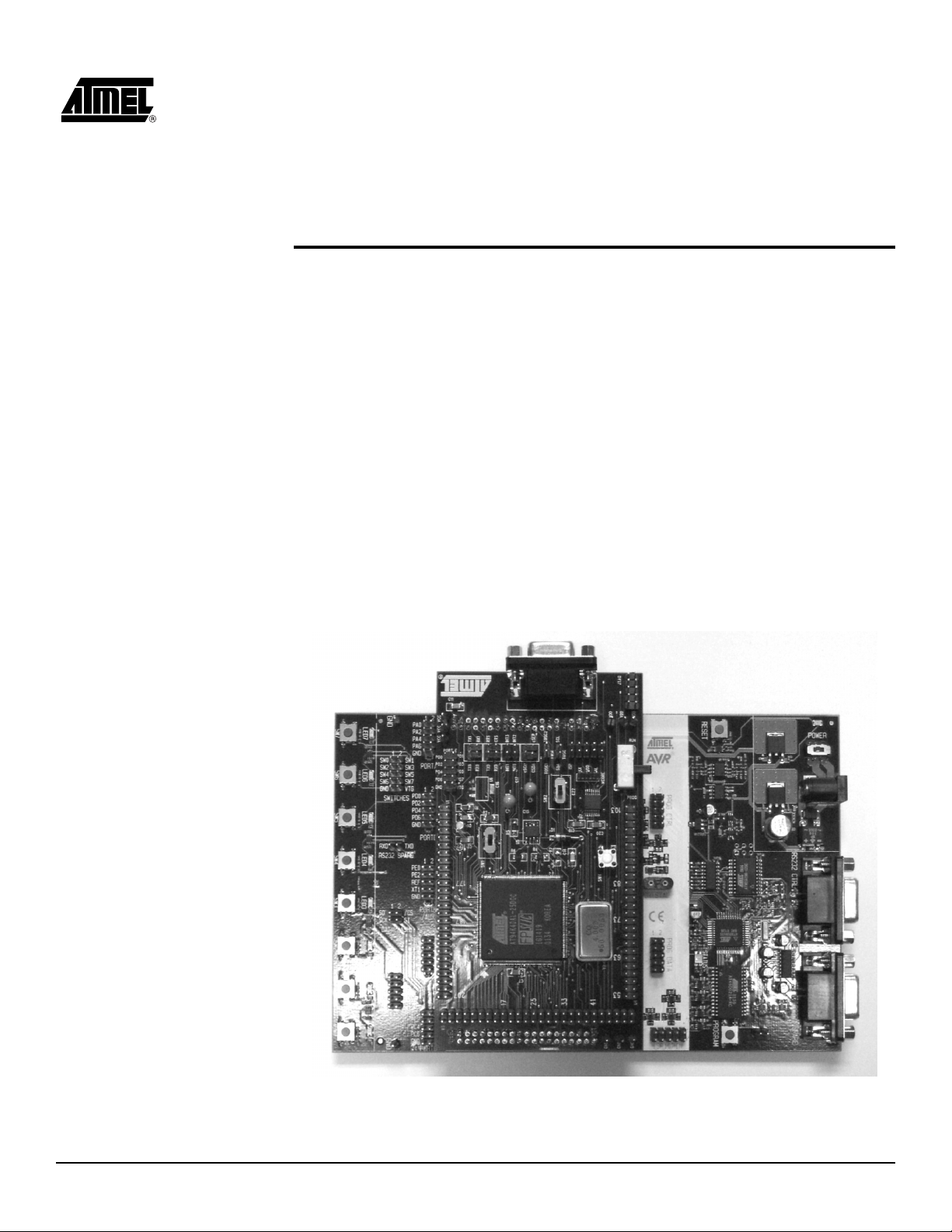
Using the STK594 Top Module.............................................................2-1
2.1 Preparing the STK500 for Use with the STK594.......................................2-1
2.1.1 Adjusting VTARGET for the AT94K Devices......................................2-1
2.1.2 Connecting the STK594 to the STK500 Starter Kit ............................2-1
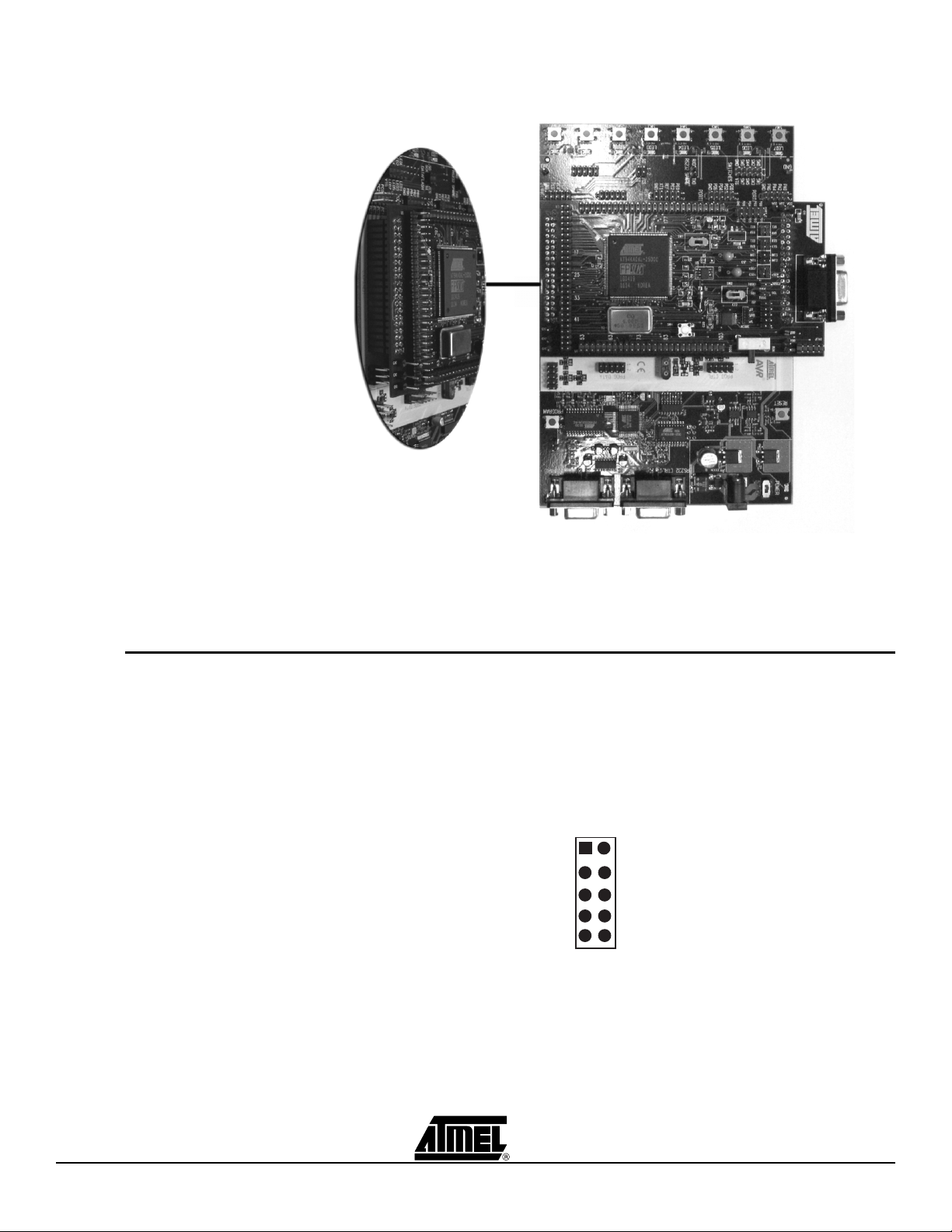
2.2 PORT Connectors.....................................................................................2-2
2.2.1 PORT E ..............................................................................................2-2
2.3 Programming the AT94K Devices.............................................................2-3
2.4 JTAG Connector .......................................................................................2-3
2.5 TOSC Switch.............................................................................................2-4
2.6 Universal Asynchronous Receiver Transmitter (UART)............................2-4
2.6.1 Second RS-232C Port ........................................................................2-4
2.7 Two-Wire Serial Interface (TWSI) .............................................................2-5
2.7.1 Description of Configuration Memory Pins .........................................2-5
2.8 External Interrupts.....................................................................................2-5
2.9 Split Power Supply Support ......................................................................2-6
2.10 XTAL Switch .............................................................................................2-6
2.11 Reset Switches .........................................................................................2-6
Section 3
Installing System Designer ...................................................................3-1
3.1 System Requirements...............................................................................3-1
3.3 Configuration Programming System (CPS) Installation ............................3-2
3.4 System Designer Licensing.......................................................................3-2
3.4.1 Requesting a System Designer License.............................................3-2
3.4.2 Configuring the System Designer License .........................................3-3
3.4.3 Testing the System Designer License ................................................3-3
3.4.4 Troubleshooting..................................................................................3-3
Section 4
Using System Designer ........................................................................4-1
4.1 Preparing the Example Files.....................................................................4-1
4.3 Design Flow ..............................................................................................4-2
4.6 Synthesizing the FPGA Source File..........................................................4-8
4.8 FPGA Place and Route...........................................................................4-11