AN-9111 APPLICATION NOTE
© 2015 Fairchild Semiconductor Corporation www.fairchildsemi.com
Rev. 1.1 6/26/15 6
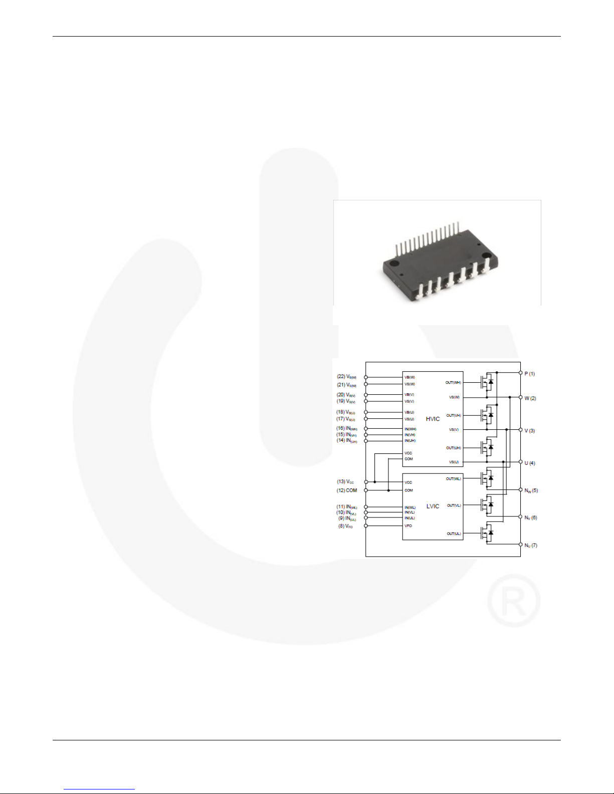
3.2. Detailed Pin Definition and Notification
High-Side Bias Voltage Pins for Driving the
MOSFET / High-Side Bias Voltage Ground
Pins for Driving the MOSFET
Pin: VB(U)-VS(U), VB(V)-VS(V), VB(W)-VS(W)
•These are drive power supply pins for providing gate
drive power to the high-side MOSFETs.
•The external power supplies dont need for the high
side MOSFET driving by using bootstrap circuit..
•Each bootstrap capacitor is charged from the VCC
supply during ON state of the corresponding low-
side MOSFET.
•To prevent malfunctions caused by noise and ripple
in the supply voltage, a low-ESR, low-ESL filter
capacitor should be mounted very close to these pins.
Low-Side Bias Voltage Pin / High-Side Bias
Voltage Pins:
Pin: VCC
•These are control supply pins for the built-in ICs.
•This pin should be connected externally.
•To prevent malfunctions caused by noise and ripple
in the supply voltage, a low-ESR, low-ESL filter
capacitor should be mounted very close to these pins.
Low-Side Common Supply Ground Pins
Pin: COM
•The common (COM) pin connects to the control
ground for the internal ICs.
•Important! To avoid noise influences, the main
power circuit current should not be allowed to blow
through this pin.
Signal Input Pins
Pin: IN(UL), IN(VL), IN(WL), IN(UH), IN(VH), IN(WH)
•These pins control the operation of the built-in
MOSFETs.
•They are activated by voltage input signals. The
terminals are internally connected to a Schmitt-
trigger circuit composed of 5 V-class CMOS.
•The signal logic of these pins is active HIGH. The
MOSFETs associated with each of these pins are
turn-on when a sufficient logic voltage is applied to
these pins.
•The wiring of each input should be as short as
possible to protect the Motion SPM®45 LV series
against noise influences.
•To prevent signal oscillations, an RC coupling as
illustrated in Figure 16 is recommended.
Fault Output Pin
Pin: VFO
•This is the fault output alarm pin. An active LOW
output is given on this pin for a fault state condition
in the SPM.
•The alarm condition is: low-side bias Under-Voltage
Lockout (UVLO).
•The VFO output is open drain configured. The VFO
signal line should be pulled to the 5 V logic power
supply with approximately 4.7
Positive DC-Link Pin
Pin: P
•This is the DC-link positive power supply pin of the
inverter.
•It is internally connected to the drains of the high-
side MOSFETs.
•To suppress surge voltage caused by the DC-link
wiring or PCB pattern inductance, connect a
smoothing filter capacitor close to this pin (tip: metal
film capacitor is typically used).
Negative DC-Link Pins
Pin: NU, NV, NW
•These are the DC-link negative power supply pins
(power ground) of the inverter.
•These pins are connected to the low-side MOSFET
source of the each phase.
•These pins are used in connection with one shunt or
three shunt resistor
Inverter Power Output Pins
Pin: U, V, W
•Inverter output pins for connecting to the inverter
load (e.g. motor).