6
Using the Board
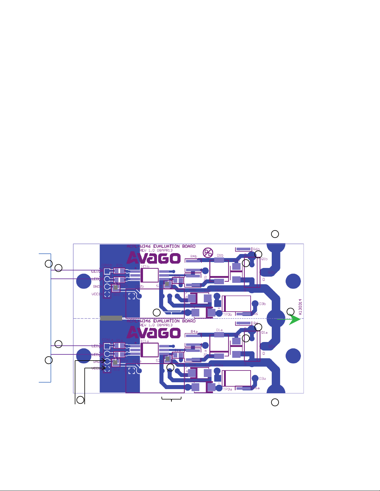
It is easy to prepare the evaluation board for use. You just need to solder cables for DC supplies, have proper cables for
HVDC+/HVDC- high voltage bus, and load connections. The evaluation board has a default connection as shown in
Table 1 when it is shipped to the customer. We oer several power supply schemes from which you can choose.
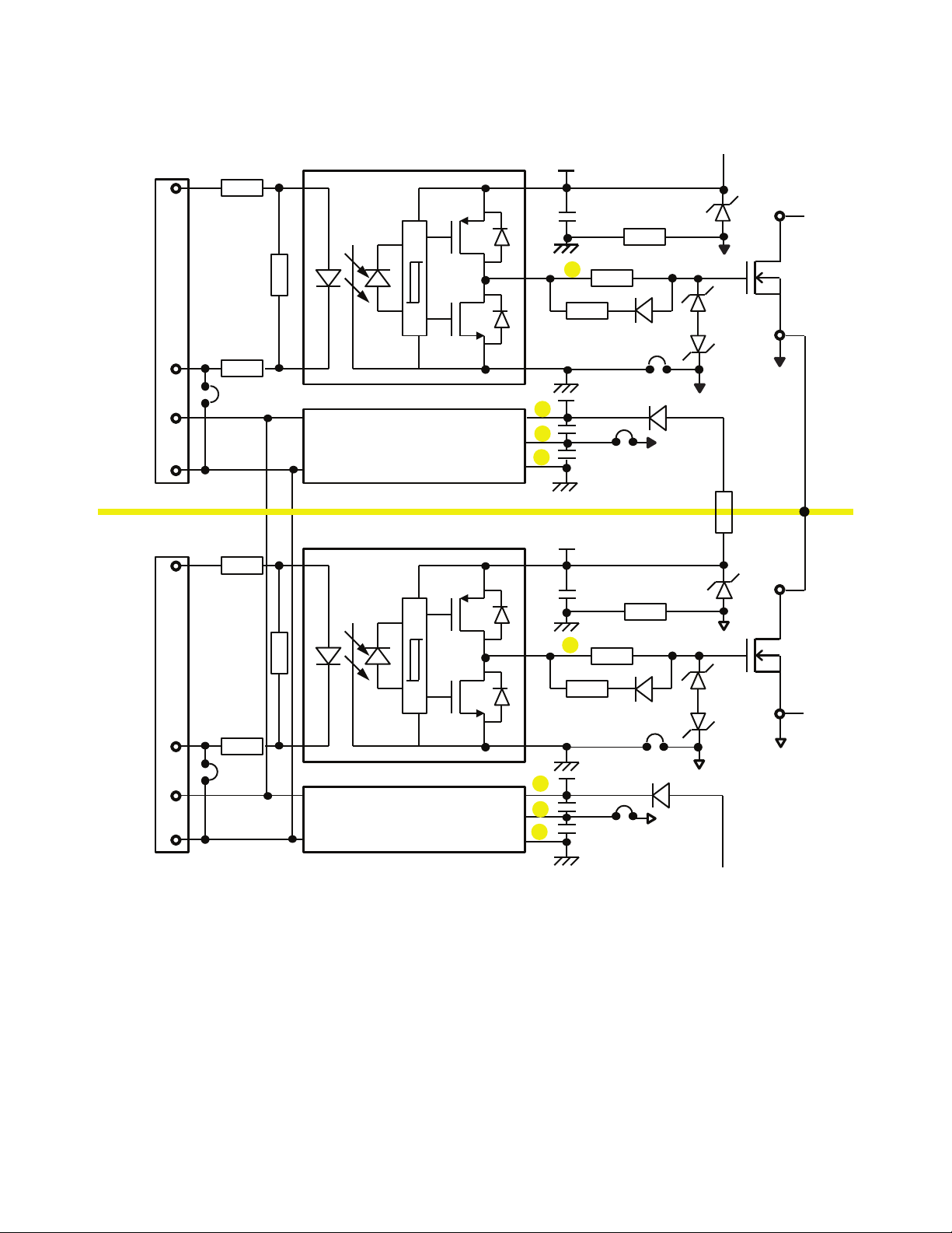
Power Supply Schemes
The evaluation board is built with DC supply exibility in mind; choose a power supply scheme from the seven available.
Table 1 shows all the possible power supply schemes that work for the evaluation board. A description of each scheme
is given; you are encouraged to explore each scheme and decide which one works best for your needs:
1. Scheme 1 is the simplest and possibly the cheapest scheme. A +5 V isolated DC supply is supplied externally to
power the low voltage Vcc1 circuit. Another external supply (+12 V~20 V for Vcc2a) is needed for the gate driver driving
the power MOSFET at the bottom inverter arm. Vcc2b supply is obtained from Vcc2a by bootstrapping. For this to
work, the bootstrap components D3b and R6 must be connected, all S2 jumpers must be shorted so that no negative
supply of Vee is allowed, and the Signal Input 2 is at 180°out of phase to Signal Input 1. All S2 jumpers are shorted to
connect Vee to Veso that there are no negative supplies. S3 jumpers are shorted by default but this has no eect on
actual operation of the board. Contact Avago Technologies if bootstrapping operation works are required.
2. Scheme 2 is similar to Scheme 1: it has Vcc1 and Vcc2a supplies. However, as the power MOSFET used gets bigger,
so does the driving power. Because a bootstrapped power supply can only handle a lower driving power, it is not
suitable for use when Qg of power MOSFET rises above 200 nanocoulombs (nC). A third external supply (+12 V~ 20
V for Vcc2b) will be needed.
3. Scheme 3 is similar to Scheme 2 in that it uses three external supplies at Vcc1, Vcc2a and Vcc2b. Scheme 3, however, has
the advantage of getting negative supplies for Vee (or Veea and Veeb) by introducing a 12 V Zener diode at D4 and R7
of around 1 kΩto provide proper biasing current at D4. For this scheme to work, both the S2 and S3 jumpers must be
open while the external supplies (+15 V ~ 24 V) on the high voltage driver side are to be connected acrossVcc2 and Vee
pins only, not the Vepin. As the external supply changes from +15 V to +24 V, Vcc2 will stay at +12V, but Vee changes
from -3 V to -12 V, all w.r.t. virtual ground at Ve.
4. Scheme 4 is another simple scheme; an alternative to Scheme 1. Here, only one external supply for Vcc1 is needed.
Vcc2a is obtained by a lower power DC/DC converter at IC2a, with Vcc1 as Vin and +12 V output at Vcc2a w.r.t. Vea. Vcc2b
supply is obtained from Vcc2a by bootstrapping. For this to work, the bootstrap components D3b and R6 must be
connected, all S2 jumpers must be shorted so that no negative supply of Vee is allowed, and the Signal Input 2 should
be 180°out of phase to Signal input 1. S2 is shorted to connect Vee to Veso that there is no negative supply. S3
jumpers are shorted by default but this has no eect on actual operation of the board.
5. Scheme 5 is similar to Scheme 4: it has Vcc1 and a DC/DC converter for Vcc2a. However, as the power MOSFET used
gets bigger, so does the driving power. Because a bootstrapped power supply can only handle a lower driving power,
it is not suitable for use when Qg of power MOSFET rises above 200 nanocoulombs (nC). A second DC/DC converter at
IC2b with Vcc1 as Vin and +12 V output at Vcc2b w.r.t .Veb. All S2 jumpers are shorted to connect Vee to Veso that there
are no negative supplies. S3 jumpers are shorted by default but this has no eect on actual operation of the board.
6. Scheme 6 is similar to Scheme 5 with the use of Vcc1 and two DC/DC converters. Each DC/DC converter, however, has
dual outputs set at ±12 V to allow for the availability of negative Vee (at Veea and Veeb). Therefore, all S2 jumpers must
be open, while all S3 jumpers must be shorted.
7. Use Scheme 7 if dual-output ±12 V DC/DC converters are not available or dual-output ±9 V DC/DC converters are
preferred. 12 V Vcc2 can still be obtained using ±9 V DC/DC converters by introducing a 12V Zener diode at D4 and R7
of around 1kΩto provide proper biasing current at D4. For this scheme to work, both the S2 and S3 jumpers must be
open. As the total voltage across Vcc2 w.r.t. Vee stays at 18V (=9V+9V), Vcc2 of 12 V will be obtained through the 12 V
D4 Zener diode, and -6V at Vee, all w.r.t. virtual ground at Ve.