manuals.online logo
Brands
  1. Home
  2. •
  3. Brands
  4. •
  5. Avago
  6. •
  7. Motherboard
  8. •
  9. Avago HCPL-4562 User manual

Avago HCPL-4562 User manual

HCPL-4562, HCNW4562
High Bandwidth, Analog/Video Optocouplers
Evaluation Kit Guide
Hardware Manual
Introduction
The HCPL-4562/HCNW4562 is the highest bandwidth ana-
log isolator in the industry. Avago Evaluation Kit is a fully
assembled PC board designed as circuit schematic in Fig-
ure1 to provide testing and evaluating tool for wideband
analog / video signal isolation with optocoupler HCPL-
4562 or HCNW4562. Simply connect input signal to the
board via input BNC connector B1, and separately a 5Volts
DC power supply and a 9 Volts DC power supply connect
to input and output side of the circuit, then output signal
are measured at output BNC connector B2.
The Evaluation Kit is RoHS compatible.
Applications
•Video isolation for the following standards/formats:
•NTSC, PAL, SECAM, S-VHS, Analog RGB
•Low drive current feedback element in switching power
supplies, e.g., for ISDN networks
•A/D converter signal isolation
•Analog signal ground isolation
•High voltage insulation
Features
•Wide bandwidth (-3dB):
17 MHz (HCPL-4562)
9 MHz (HCNW4562)
•High voltage gain:
2.0 (HCPL-4562)
3.0 (HCNW4562)
•Low GV temperature coecient: -0.3%/°C
•Highly linear at low drive currents
•High-speed AlGaAs emitter
•Safety approval:
Optocoupler UL Recognized
3750 V rms for 1 minute (5000 V rms for 1 minute
for HCPL-4562#020 and HCNW4562) per UL 1577
CSA Approved
IEC/EN/DIN EN 60747-5-2 Approved
VIORM = 1414 V peak for HCNW4562
•Available in 8-pin DIP and widebody packages
Recommended Equipment
•5VDC Power Supply
•9VDC Power Supply
•Functional / Analog Signal Generator
•Measurement Equipments: Oscilloscope, Voltmeter
2
Quick Start Procedure
The HCPL-4562/HCNW4562 Evaluation Kit is fully assem-
bled and tested. Following procedures guide you to oper-
ate this board.
This kit is recommended for optocoupler evaluation and
application reference only, Avago Technologies cannot
assume responsibility for use of any circuitry other than
circuitry entirely embodied in this board. No circuit patent
licenses are implied.
1. Verify there should not be any interconnection
between input and output side circuits.
2. Verify both 5 VDC and 9 VDC power supply are set
right voltage output, do not turn on any power supply
before all are connected. The Evaluation Kit both
power supplies are recommended within maximum
15 VDC.
3. Connect 5 VDC power supply to input side J1, and 9
VDC power supply to output side J2.
4. Connect input signal from signal generator to B1, and
measurement equipment oscilloscope to B2. Don’t
turn on output of signal generator.
5. Turn on 5 VDC power supply.
6. Measure voltage at point VB and VE, VB is around 1.15
V and VE around 0.5 V.
7. Turn on 9 VDC power supply.
8. Turn on signal generator output, adjust oscilloscope
setting to measure output waveform. This circuit is
designed for a typical 1 Vp-p input signal.
9. Adjust resistor R4 get desired gain GV.
10. The Kit is designed AC output signal with C2= 2.2
µF capacitor coupling, when JU1 is shorted with a
shunt, the output signal is DC coupled. DC coupling is
recommended if it is acceptable in design system. Or
user can apply AC coupling via other capacitor with
JU1 shorted.
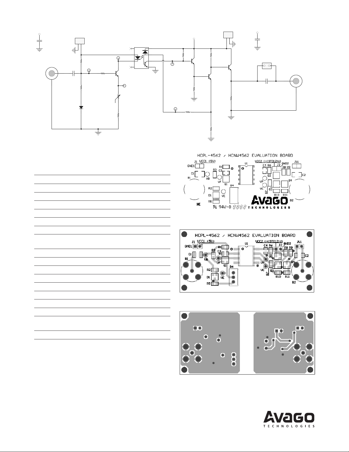
Detailed Description
Figure 1 shows a schematic circuit for wide-bandwidth
analog/video application and an amplier design. This is
an ac input coupled and ac output coupled circuit. The
LED input current IF is set at a recommended 6 mA for the
HCPL-4562 or 10 mA for the HCNW4562 by selecting an
appropriate value for the R4. If the VCC1 on the input side
is 5 V the voltage VB established by the resistor divider R1
and R2 at the base of Q1 (neglecting base current drop
across R3) is approx. 1.15 V. This establishes the voltage
VE at the emitter of Q1 around 0.5 V. Adjust R4 to set the
recommended LED current at 6 mA. With 0.5 V at VE the
resistor R4 is selected to be approx. 70 Ω for 6 mA of IF.
For isolating a composite video signal, VCC1 is recom-
mended increasing to 9V so that transistor Q1 has higher
bias voltage VB, and R4 can have more space to be ad-
justed.
With a VCC2 supply between 9 to 12 V, the value of R11
is selected to keep the output voltage at midpoint of the
supply at approx. 4.25 V with the collector current ICQ4 of
Q4 at approx. 9 mA.
ICQ4 ≈Vo/R11 ≤4.25V/470 Ω ≤9 mA
The small signal model of the bipolar transistors can de-
termine the overall voltage gain of the circuit and gain
stages involved and is found to be
GV≈VOUT/ VIN
≈∂IPB/∂IF[R7R9/(R4R10)]
Where ∂IPB/∂IFis the base photo current gain (photo di-
ode current gain) and is indicated as a typical of 0.0032 in
the data sheet.
Adjust resistor R4to achieve the desired voltage gain.
The voltage gain of the second stage (Q3) is approximate-
ly equal to
R9/ R10 • / [1 + sR9(CCQ3 +1/(2pR11' fT4) )]
Where R11' is the parallel combination of R11 and load
impedance and fT4 is the unity gain frequency Q4. From
this equation one can observe that to maximize the band-
width one would want to increase the value of R11' or re-
duce the value of R9at a constant ratio of R9/R10.
For product information and a complete list of distributors, please go to our web site: www.avagotech.com
Avago, AvagoTechnologies, and the A logo are trademarks of AvagoTechnologies in the United States and other countries.
Data subject to change. Copyright © 2005-2008 AvagoTechnologies. All rights reserved.
AV02-1138EN - October 23, 2008
Table 1. Component List
Designator Part Type Description
R2,R8 1K Resistor
R6 9.1K Resistor
R7 15K Resistor
R9 750 Resistor
C3,C4 0.1µF Chip Capacitor
D1 BAS16 Switching Diode, NXP
Q1,Q2,
Q3,Q4
MMBT3904 NPN Transistor, On Semi
C1 47µF/16V Ceramic Capacitor
C2 2.2µF/50V Ceramic Capacitor
R4 51R Resistor
R1 6.8K Resistor
R11 470R Resistor
B1 B2 75WConnector BNC Jack
R3, R10 100R Resistor
VR1 500R Variable Resistor
U1 HCPL-4562 /
HCNW4562
Optocoupler,
Avago Technologies
J1, J2, JU1 2-Pin Header 2.54 Pitch SIL
Figure 1. HCPL-4562 / HCNW4562 Evaluation Circuit Schematic
Figure 2. HCPL-4562 / HCNW4562 Evaluation Kit PCB Silkscreen
Figure 3. HCPL-4562 / HCNW4562 Evaluation Kit PCB Top Overlay
Figure 4. HCPL-4562 / HCNW4562 Evaluation Kit PCB Bottom Overlay
R1
6.8k
R2
1.0K
R3
100R
R5
51R
3
2
C6
E5
1
4
8
7
KPD
U1
HC NW 4562 / HC PL-4562
R4
500
C 3
0.1uF
R6
9.1K
R7
15K
R9
750
R10
100
R8
1.0K
R11
470
VE
13
D1
BA S 16
VF
GND1
GND1
Q1
MMBT 3904
C 4
0.1uF
V C C 2
GND2
GND2
VC
Q2
MMBT 3904
+5V
Q3
MMBT 3904
Q4
MMBT 3904
GND2
VP
GND2
GND2
+(9 T O 12 ) V
1 2
JU1
VB
1
2
B2
1
2
B1 C 2
2.2 uF / 50V
C 1
47uF / 16V
VIN
VOUT
1
2
J1
GND1
1
2
J2
GND2
V C C 1 (5V)GND 1
VC C2 +(9 TO 12 ) V GND2
V C C 1 (5V )

This manual suits for next models

1

Other Avago Motherboard manuals

Avago ACNT-H313 User manual

Avago

Avago ACNT-H313 User manual

Avago AFBR-800EVK User manual

Avago

Avago AFBR-800EVK User manual

Avago HEDS-8937 User manual

Avago

Avago HEDS-8937 User manual

Avago ACPL-C79B User manual

Avago

Avago ACPL-C79B User manual

Avago ACPL-P349 User manual

Avago

Avago ACPL-P349 User manual

Avago ACPL-P346 User manual

Avago

Avago ACPL-P346 User manual

Popular Motherboard manuals by other brands

ECS P4ITA2 manual

ECS

ECS P4ITA2 manual

Asus Crosshair V Formula ThunderBolt user manual

Asus

Asus Crosshair V Formula ThunderBolt user manual

MSI Wind Board D510 Series manual

MSI

MSI Wind Board D510 Series manual

ASROCK Rack WC621D8A-2T user manual

ASROCK Rack

ASROCK Rack WC621D8A-2T user manual

ASROCK 4Core1333-eSATA2 manual

ASROCK

ASROCK 4Core1333-eSATA2 manual

Texas Instruments TPL7407L7 user guide

Texas Instruments

Texas Instruments TPL7407L7 user guide

SOLTEK SL-845GVI manual

SOLTEK

SOLTEK SL-845GVI manual

Texas Instruments LMG2100 user guide

Texas Instruments

Texas Instruments LMG2100 user guide

National Semiconductor LM64 user guide

National Semiconductor

National Semiconductor LM64 user guide

Abit BG7E user manual

Abit

Abit BG7E user manual

AMS TSL2540 EVM user guide

AMS

AMS TSL2540 EVM user guide

Analog Devices ADuC7026 reference guide

Analog Devices

Analog Devices ADuC7026 reference guide

Maxim MAX16920A General description

Maxim

Maxim MAX16920A General description

ST STEVAL-BTDP1 user manual

ST

ST STEVAL-BTDP1 user manual

Texas Instruments TPS53129EVM-621 user guide

Texas Instruments

Texas Instruments TPS53129EVM-621 user guide

VIA Technologies VB8004 user manual

VIA Technologies

VIA Technologies VB8004 user manual

Gigabyte MS73-HB2 user manual

Gigabyte

Gigabyte MS73-HB2 user manual

Avalue Technology EAX-C246P-B1 user manual

Avalue Technology

Avalue Technology EAX-C246P-B1 user manual

manuals.online logo
manuals.online logoBrands
  • About & Mission
  • Contact us
  • Privacy Policy
  • Terms and Conditions

Copyright 2025 Manuals.Online. All Rights Reserved.